Lecture: Integration of silicon photonics with electronics. Prepared by Jean-Marc FEDELI CEA-LETI
|
|
|
- Chrystal Walker
- 5 years ago
- Views:
Transcription
1 Lecture: Integration of silicon photonics with electronics Prepared by Jean-Marc FEDELI CEA-LETI
2 Context The goal is to give optical functionalities to electronics integrated circuit (EIC) The objectives are either: Increase the performance of photonics with embedded electronic Increase the data transmission speed between cores with photonics 2
3 Some goals Minimum impact on EIC designer librairies Development of a specific designer CMOS libraries require a huge effort ( ). So integration of optical components requires minimum change of a design library Wafer testability with high throughput Optical devices on a EIC chip have to be tested with the same procedures as electronic devices. So full wafer testability without any dicing, polishing, assembly Lowest added process complexity This is an issue related to yield, so cost ( ) 3
4 Integration of Si Photonics on EIC?? Pads Mn BE: Back end FE:Front end Transistors M1 Si substrate 4

5 Die flip-chip solution Source PD e=3µm SiO2 BOX Silicon substrate SiO2 BOX Silicon substrate Photonic wafer fabrication Die substrate Not a wafer level fabrication Uncompatibility with microelectronics packaging Could be a good solution for low volume Flip chip bonding on CMOS dies or wafer 5

6 KOTURA example 6
7 Integration of photonics on CMOS Option 2 Combined front-end fabrication 7
8 Combined fabrication Micro-electronics Bulk Technologies (CMOS, BiCMOS, SiGe, etc ) SOI Technology evolution: thin Si upper layer 55nm on BOX 145nm Photonics SOI wafers with Si 200 to 400nm on BOX> 1µm 8
9 Which substrate for combined fabrication? Si upper layer photonics BOX SOI photonics Adapt electronics library to thicker box Si Substrate photonics area photonics BOX SOI electronics area electronics BOX Dedicated area for photonics and electronics Cost? Bulk electronics area photonics area photonics BOX Buried thick BOX on a bulk substrate Cost and quality? 9


10 Option 2: Luxtera approach Proprietary SOI CMOS 130nm technology Proprietary library for IC design Flip chip bonded lasers or external WDM lasers Surface gratings fiber couplers MUX and DEMUX with controlled MMI 10Gb/s modulator based on lateral Si depletion 20GHz Ge photodetectors Electronic control of optical devices 10

11 Option 2: Combined fabrication( Luxtera) SOI? WG width and thickness? Pitch of the grating? Partial etching for the grating? 11

12 Option 2: Combined fabrication( Luxtera) MODULATOR The gray-scale gradient in the figure indicates that the doping density varies laterally from low doping at the junction to high doping at the contact region. This design is the result of a tradeoff between minimizing optical insertion loss due to the presence of free carriers overlapping the optical mode (desire for low doping density) and minimizing the series resistance of the diode (desire for high-doping density). LUXTERA 12

13 Option 2: Combined fabrication( Luxtera) Ge epitaxy in a CVD environment is, usually, naturally selective to oxide When it comes to choose the insertion point of the Ge epitaxy step within a CMOS process, several factors must be considered: the temperature profile of the process, the possibility to contact the Ge device using the standard Si contact module, the salicide sensitivity to thermal treatments, the availability of a clean Si surface, the presence of dielectric films and their interaction on the selective growth of Ge. All these requirements may differ among different technology nodes (Luxtera) 13

14 Lightwire Integration of on optical modulator 14
15 15
16 16

17 MIT Eos1 65 nm test chip Texas Instruments standard 65 nm bulk CMOS process First ever photonic chip in sub-100nm CMOS Automated photonic device layout Monolithic integration with electrical modulator drivers 17


18 MIT Eos1 65 nm test chip Ring modulator Digital driver Two-ring filter Vertical coupler grating One-ring filter Paperclips Photo detector Waveguide crossings M-Z test structures 4 ring filter banks 18


19 MIT Eos1 65 nm test chip Cross-sectional view of a photonic chip SEM image of a poly silicon waveguide Waveguide made of polysilicon Silicon substrate under waveguide etched away to provide optical cladding 64 wavelengths per waveguide in opposite directions 19
20 Option 1: Integration above metallization Photonic layer at the last levels of metallizations with back-end fabrication 1A: Wafer bonding of PIC processed at high temperature on SOI 1B: Back-end fabrication of PIC at low temperature 20
21 Option 2B with low T c technology Source PD SiN or a:si Waveguide formation with SiO2 cladding Bonding InP dies Source PD Connection with EIC through passivation layers Fabrication of source and PD 21

 2 db/cm Bend (R 25µm) 0.")
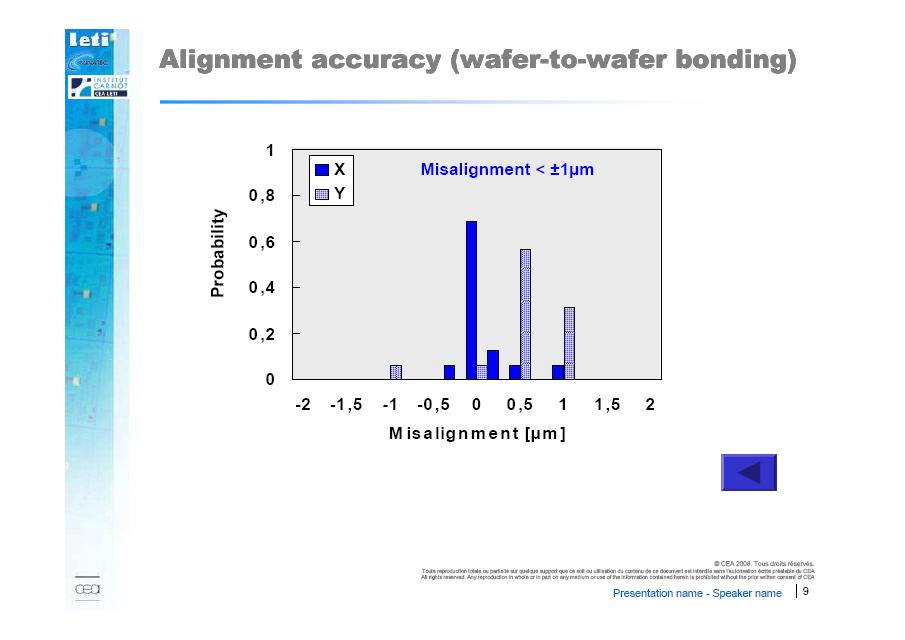
 1 => 4 MMI 1.4dB ( E<0.")
22 SiNx waveguides at low temperature Fabrication at 350 C, Cladding with SiO2 Si 3 N 4 Losses Waveguide (0.4µm x 0.8µm) 2 db/cm Bend (R 25µm) 0.02 db/90 µbend Y junction 1.1 db 1 => 2 MMI 0.5 db ( E<0.2dB) 1 => 4 MMI 1.4dB ( E<0.45dB) 1 to 16 distribution network E<0.5dB 22

23 Option 1: Integration above metallization Photonic layer at the last levels of metallizations with back-end fabrication 1A: Wafer bonding of PIC processed at high temperature on SOI 1B: Back-end fabrication of PIC at low temperature 23
24 Electronic-Photonic Integration CMOS wafer planarized Deposition of SiO2 layer for bonding CMOS wafer transistors metal interconnects 24
25 Rib Silicon Photonic layer SOI 400nm / 2000 nm Litho FC + transition Rib strip : Rib Waveguide definition Si etching 180nm FC 25
26 Stripe Silicon Photonic layer Litho Passive 220nm: AWG, RR, etc.: Stripe Waveguide definition Si etching 220nm FC AWG 26
27 Modulator Processing Lithos for implantation Different implantations FC Modulator AWG 27
28 Ge photodetector Processing Cavity formation Ge epitaxy in cavity P & N Implant FC Modulator AWG Ge PD 28
29 Planarization SiO2 deposition 1µm Planarization FC Modulator AWG Ge PD 29
30 Molecular wafer bonding Alignement of the two wafers (+-2µm) Molecular bonding of photonic wafer on CMOS wafer CMOS wafer transistors metal interconnects 30
31 31
32 Substrate removal Mechanical grinding Si chemical etching FC Modulator AWG Ge PD CMOS wafer transistors metal interconnects 32
33 InP heterostructure bonding bond small InP dice with herostructure on wafer InP substrate removal of dice FC Modulator AWG Ge PD CMOS wafer transistors metal interconnects 33
34 InP heterostructure process Process InP source (InP etching) Planarized with SiO2 FC InP source Modulator AWG Ge PD CMOS wafer transistors metal interconnects 34
35 Vias formation Lithos for different depths Etching SiO2 FC InP source Modulator AWG Ge PD CMOS wafer transistors metal interconnects 35
36 Metal formation Metal deposition Metal etching PAD FC InP source Modulator AWG Ge PD CMOS wafer transistors metal interconnects 36


37 SOI wafer bonded on a CMOS wafer Silicon rib waveguide Germanium 37


38 Monocristalline rib waveguide with Ge in cavity Silicon Ge cavity SiO 2 Metallisations Silicon rib waveguide 38
39 Photonic wafer metallic bonded on EIC wafer Source PD SiO2 BOX Silicon substrate SiO2 BOX Silicon substrate Photonic wafer Photonic functions with high temp technology Die to wafer source bonding Substrate removal Metallic bonding Planarized electrodes formation 39

 0,04 0,03 0,02 0,01 0,00-0,01-0,1 0,0 0,1 0,2 0,3 0,4 0,5 0,6 0,7 0,8 0,9 1,0 1,1")
40 Wafer bonding Cu/Cu of CMOS with SOI photonics Process independantly SOI photonics wafer and CMOS wafer Finish with Cu pad interface Cu-Cu bond at low temperature the two wafers Remove the SOI photonics substrate Contact on the electronics pad by the top surface is not easy 0,08 0,07 0,06 0,05 V(Volt) 0,04 0,03 0,02 0,01 0,00-0,01-0,1 0,0 0,1 0,2 0,3 0,4 0,5 0,6 0,7 0,8 0,9 1,0 1,1 I(Ampere) 40
41 Photonic wafer thinned bonded on EIC wafer with TSV Source PD Photonic wafer Die to wafer source bonding Active device fabrication Bonding a handle wafer and thinning the PIC substrate Through Silicon Vias formation Removal of the handle wafer Bonding EIC with PIC 41
42 42

43 Option 1A approachs MIT technology Concept of BE technology with SiGe 43

44 Integration of a photonic layer by IBM 44
45 IBM 2 45
46 IBM 3 46
47 Integration HP Labs 47
48 Integration of photonics on CMOS Option 1 Photonic layer at the last levels of metallizations with back-end fabrication Option 2 Combined front-end fabrication Option 3 Backside fabrication BE: Back end FE:Front end 48
49 Option 3: Low T C fabrication on the back side Si Substrate Si Substrate Si Substrate a:si Waveguide on backside of CMOS wafer InGaAsPD Fab of InP components Connection with CMOS through the substrate Fabrication of the EIC Protection of the Front side Process of the Back side (needs double side polished) Low temperature technology for photonics components a:si wg InP laser InGaAs photodetectors Vias through the Si substrate 49
50 Option 3: Wafer bonding on the back side Fabrication of the EIC Protection of the Front side Fabrication of the PIC Wafer bonding of an PIC on the rear side of an EIC Removal of the Si substrate of the PIC Vias through the Si substrate (TSV) Si Substrate Si Substrate Si Substrate Si Substrate 50
51 Conclusion No unique integration technology Need of integration depends on the targeted applications Hybrid technology for small volume Full integration for medium to large volume Integration of exotic materials possible with AIC 51
Si and InP Integration in the HELIOS project
 Si and InP Integration in the HELIOS project J.M. Fedeli CEA-LETI, Grenoble ( France) ECOC 2009 1 Basic information about HELIOS HELIOS photonics ELectronics functional Integration on CMOS www.helios-project.eu
IEEE JOURNAL OF SELECTED TOPICS IN QUANTUM ELECTRONICS 2010 Silicon Photonic Circuits: On-CMOS Integration, Fiber Optical Coupling, and Packaging
 IEEE JOURNAL OF SELECTED TOPICS IN QUANTUM ELECTRONICS 2010 Silicon Photonic Circuits: On-CMOS Integration, Fiber Optical Coupling, and Packaging Christophe Kopp, St ephane Bernab e, Badhise Ben Bakir,
Silicon Photonics Technology Platform To Advance The Development Of Optical Interconnects
 Silicon Photonics Technology Platform To Advance The Development Of Optical Interconnects By Mieke Van Bavel, science editor, imec, Belgium; Joris Van Campenhout, imec, Belgium; Wim Bogaerts, imec s associated
NEXT GENERATION SILICON PHOTONICS FOR COMPUTING AND COMMUNICATION PHILIPPE ABSIL
 NEXT GENERATION SILICON PHOTONICS FOR COMPUTING AND COMMUNICATION PHILIPPE ABSIL OUTLINE Introduction Platform Overview Device Library Overview What s Next? Conclusion OUTLINE Introduction Platform Overview
A 3.9 ns 8.9 mw 4 4 Silicon Photonic Switch Hybrid-Integrated with CMOS Driver
 A 3.9 ns 8.9 mw 4 4 Silicon Photonic Switch Hybrid-Integrated with CMOS Driver A. Rylyakov, C. Schow, B. Lee, W. Green, J. Van Campenhout, M. Yang, F. Doany, S. Assefa, C. Jahnes, J. Kash, Y. Vlasov IBM
Envisioning the Future of Optoelectronic Interconnects:
 Envisioning the Future of Optoelectronic Interconnects: The Production Economics of InP and Si Platforms for 100G Ethernet LAN Transceivers Shan Liu Dr. Erica Fuchs Prof. Randolph Kirchain MIT Microphotonics
Silicon Photonics: an Industrial Perspective
 Silicon Photonics: an Industrial Perspective Antonio Fincato Advanced Programs R&D, Cornaredo, Italy OUTLINE 2 Introduction Silicon Photonics Concept 300mm (12 ) Photonic Process Main Silicon Photonics
Index. Cambridge University Press Silicon Photonics Design Lukas Chrostowski and Michael Hochberg. Index.
 absorption, 69 active tuning, 234 alignment, 394 396 apodization, 164 applications, 7 automated optical probe station, 389 397 avalanche detector, 268 back reflection, 164 band structures, 30 bandwidth
VERSATILE SILICON PHOTONIC PLATFORM FOR DATACOM AND COMPUTERCOM APPLICATIONS. B Szelag CEA-Leti
 VERSATILE SILICON PHOTONIC PLATFORM FOR DATACOM AND COMPUTERCOM APPLICATIONS B Szelag CEA-Leti OUTLINE Silicon photonic : 200mm CMOS core technology towards 300mm Emergent needs vs core process Technological
Silicon Photonics in Optical Communications. Lars Zimmermann, IHP, Frankfurt (Oder), Germany
, Germany") Silicon Photonics in Optical Communications Lars Zimmermann, IHP, Frankfurt (Oder), Germany Outline IHP who we are Silicon photonics Photonic-electronic integration IHP photonic technology Conclusions
Silicon Photonics in Optical Communications Lars Zimmermann, IHP, Frankfurt (Oder), Germany Outline IHP who we are Silicon photonics Photonic-electronic integration IHP photonic technology Conclusions
Silicon Photonics Photo-Detector Announcement. Mario Paniccia Intel Fellow Director, Photonics Technology Lab
 Silicon Photonics Photo-Detector Announcement Mario Paniccia Intel Fellow Director, Photonics Technology Lab Agenda Intel s Silicon Photonics Research 40G Modulator Recap 40G Photodetector Announcement
Electronic-Photonic ICs for Low Cost and Scalable Datacenter Solutions
 Electronic-Photonic ICs for Low Cost and Scalable Datacenter Solutions Christoph Theiss, Director Packaging Christoph.Theiss@sicoya.com 1 SEMICON Europe 2016, October 27 2016 Sicoya Overview Spin-off from
High-speed Ge photodetector monolithically integrated with large cross silicon-on-insulator waveguide
 [ APPLIED PHYSICS LETTERS ] High-speed Ge photodetector monolithically integrated with large cross silicon-on-insulator waveguide Dazeng Feng, Shirong Liao, Roshanak Shafiiha. etc Contents 1. Introduction
Silicon Photonics: A Platform for Integration, Wafer Level Assembly and Packaging
 Silicon Photonics: A Platform for Integration, Wafer Level Assembly and Packaging M. Asghari Kotura Inc April 27 Contents: Who is Kotura Choice of waveguide technology Challenges and merits of Si photonics
Silicon Photonics Opportunity, applications & Recent Results
 Silicon Photonics Opportunity, applications & Recent Results Dr. Mario Paniccia Intel Fellow Director, Photonics Technology Lab Intel Corporation www.intel.com/go/sp Purdue University Oct 5 2007 Agenda
New advances in silicon photonics Delphine Marris-Morini
 New advances in silicon photonics Delphine Marris-Morini P. Brindel Alcatel-Lucent Bell Lab, Nozay, France New Advances in silicon photonics D. Marris-Morini, L. Virot*, D. Perez-Galacho, X. Le Roux, D.
Convergence Challenges of Photonics with Electronics
 Convergence Challenges of Photonics with Electronics Edward Palen, Ph.D., P.E. PalenSolutions - Optoelectronic Packaging Consulting www.palensolutions.com palensolutions@earthlink.net 415-850-8166 October
Silicon photonics with low loss and small polarization dependency. Timo Aalto VTT Technical Research Centre of Finland
 Silicon photonics with low loss and small polarization dependency Timo Aalto VTT Technical Research Centre of Finland EPIC workshop in Tokyo, 9 th November 2017 VTT Technical Research Center of Finland
Alternatives to standard MOSFETs. What problems are we really trying to solve?
 Alternatives to standard MOSFETs A number of alternative FET schemes have been proposed, with an eye toward scaling up to the 10 nm node. Modifications to the standard MOSFET include: Silicon-in-insulator
64 Channel Flip-Chip Mounted Selectively Oxidized GaAs VCSEL Array
 64 Channel Flip-Chip Mounted Selectively Oxidized GaAs VCSEL Array 69 64 Channel Flip-Chip Mounted Selectively Oxidized GaAs VCSEL Array Roland Jäger and Christian Jung We have designed and fabricated
Silicon Photonics Transceivers for Hyper Scale Datacenters: Deployment and Roadmap
 Silicon Photonics Transceivers for Hyper Scale Datacenters: Deployment and Roadmap Peter De Dobbelaere Luxtera Inc. 09/19/2016 Luxtera Proprietary www.luxtera.com Luxtera Company Introduction $100B+ Shift
High speed silicon-based optoelectronic devices Delphine Marris-Morini Institut d Electronique Fondamentale, Université Paris Sud
 High speed silicon-based optoelectronic devices Delphine Marris-Morini Institut d Electronique Fondamentale, Université Paris Sud Data centers Optical telecommunications Environment Interconnects Silicon
Microphotonics Readiness for Commercial CMOS Manufacturing. Marco Romagnoli
 Microphotonics Readiness for Commercial CMOS Manufacturing Marco Romagnoli MicroPhotonics Consortium meeting MIT, Cambridge October 15 th, 2012 Passive optical structures based on SOI technology Building
Opportunities and challenges of silicon photonics based System-In-Package
 Opportunities and challenges of silicon photonics based System-In-Package ECTC 2014 Panel session : Emerging Technologies and Market Trends of Silicon Photonics Speaker : Stéphane Bernabé (Leti Photonics
Heinrich-Hertz-Institut Berlin
 NOVEMBER 24-26, ECOLE POLYTECHNIQUE, PALAISEAU OPTICAL COUPLING OF SOI WAVEGUIDES AND III-V PHOTODETECTORS Ludwig Moerl Heinrich-Hertz-Institut Berlin Photonic Components Dept. Institute for Telecommunications,,
Foundry processes for silicon photonics. Pieter Dumon 7 April 2010 ECIO
 Foundry processes for silicon photonics Pieter Dumon 7 April 2010 ECIO Photonics Research Group http://photonics.intec.ugent.be epixfab Prototyping Training Multi project wafer access to silicon photonic
Integrated diodes. The forward voltage drop only slightly depends on the forward current. ELEKTRONIKOS ĮTAISAI
 1 Integrated diodes pn junctions of transistor structures can be used as integrated diodes. The choice of the junction is limited by the considerations of switching speed and breakdown voltage. The forward
OPTI510R: Photonics. Khanh Kieu College of Optical Sciences, University of Arizona Meinel building R.626
 OPTI510R: Photonics Khanh Kieu College of Optical Sciences, University of Arizona kkieu@optics.arizona.edu Meinel building R.626 Announcements Homework #3 is due today No class Monday, Feb 26 Pre-record
Fabricating 2.5D, 3D, 5.5D Devices
 Fabricating 2.5D, 3D, 5.5D Devices Bob Patti, CTO rpatti@tezzaron.com Tezzar on Semiconduct or 04/15/2013 1 Gen4 Dis-Integrated 3D Memory DRAM layers 42nm node 2 million vertical connections per lay per
Progress Towards Computer-Aided Design For Complex Photonic Integrated Circuits
 Department of Electrical and Computer Engineering Progress Towards Computer-Aided Design For Complex Photonic Integrated Circuits Wei-Ping Huang Department of Electrical and Computer Engineering McMaster
OPTICAL I/O RESEARCH PROGRAM AT IMEC
 OPTICAL I/O RESEARCH PROGRAM AT IMEC IMEC CORE CMOS PHILIPPE ABSIL, PROGRAM DIRECTOR JORIS VAN CAMPENHOUT, PROGRAM MANAGER SCALING TRENDS IN CHIP-LEVEL I/O RECENT EXAMPLES OF HIGH-BANDWIDTH I/O Graphics
Integrated Photonics using the POET Optical InterposerTM Platform
 Integrated Photonics using the POET Optical InterposerTM Platform Dr. Suresh Venkatesan CIOE Conference Shenzhen, China Sept. 5, 2018 POET Technologies Inc. TSXV: PUBLIC POET PTK.V Technologies Inc. PUBLIC
Dries Van Thourhout IPRM 08, Paris
 III-V silicon heterogeneous integration ti Dries Van Thourhout IPRM 08, Paris InP/InGaAsP epitaxial layer stack Si WG DVS- BCB SiO 2 200nm III-V silicon heterogeneous integration ti Dries Van Thourhout
CMP for More Than Moore
 2009 Levitronix Conference on CMP Gerfried Zwicker Fraunhofer Institute for Silicon Technology ISIT Itzehoe, Germany gerfried.zwicker@isit.fraunhofer.de Contents Moore s Law and More Than Moore Comparison:
Silicon photonics on 3 and 12 μm thick SOI for optical interconnects Timo Aalto VTT Technical Research Centre of Finland
 Silicon photonics on 3 and 12 μm thick SOI for optical interconnects Timo Aalto VTT Technical Research Centre of Finland 5th International Symposium for Optical Interconnect in Data Centres in ECOC, Gothenburg,
CMOS Digital Integrated Circuits Lec 2 Fabrication of MOSFETs
 CMOS Digital Integrated Circuits Lec 2 Fabrication of MOSFETs 1 CMOS Digital Integrated Circuits 3 rd Edition Categories of Materials Materials can be categorized into three main groups regarding their
EE 330 Lecture 7. Design Rules. IC Fabrication Technology Part 1
 EE 330 Lecture 7 Design Rules IC Fabrication Technology Part 1 Review from Last Time Technology Files Provide Information About Process Process Flow (Fabrication Technology) Model Parameters Design Rules
Integration of Optoelectronic and RF Devices for Applications in Optical Interconnect and Wireless Communication
 Integration of Optoelectronic and RF Devices for Applications in Optical Interconnect and Wireless Communication Zhaoran (Rena) Huang Assistant Professor Department of Electrical, Computer and System Engineering
Chapter 3: Basics Semiconductor Devices and Processing 2006/9/27 1. Topics
 Chapter 3: Basics Semiconductor Devices and Processing 2006/9/27 1 Topics What is semiconductor Basic semiconductor devices Basics of IC processing CMOS technologies 2006/9/27 2 1 What is Semiconductor
SAMPLE SLIDES & COURSE OUTLINE. Core Competency In Semiconductor Technology: 2. FABRICATION. Dr. Theodore (Ted) Dellin
 Dellin") & Digging Deeper Devices, Fabrication & Reliability For More Info:.com or email Dellin@ieee.org SAMPLE SLIDES & COURSE OUTLINE In : 2. A Easy, Effective, of How Devices Are.. Recommended for everyone who
& Digging Deeper Devices, Fabrication & Reliability For More Info:.com or email Dellin@ieee.org SAMPLE SLIDES & COURSE OUTLINE In : 2. A Easy, Effective, of How Devices Are.. Recommended for everyone who
Hybrid Integration Technology of Silicon Optical Waveguide and Electronic Circuit
 Hybrid Integration Technology of Silicon Optical Waveguide and Electronic Circuit Daisuke Shimura Kyoko Kotani Hiroyuki Takahashi Hideaki Okayama Hiroki Yaegashi Due to the proliferation of broadband services
Lecture 4 INTEGRATED PHOTONICS
 Lecture 4 INTEGRATED PHOTONICS What is photonics? Photonic applications use the photon in the same way that electronic applications use the electron. Devices that run on light have a number of advantages
Silicon-On-Insulator based guided wave optical clock distribution
 Silicon-On-Insulator based guided wave optical clock distribution K. E. Moselund, P. Dainesi, and A. M. Ionescu Electronics Laboratory Swiss Federal Institute of Technology People and funding EPFL Project
Contents Silicon Photonic Wire Waveguides: Fundamentals and Applications
 1 Silicon Photonic Wire Waveguides: Fundamentals and Applications.. 1 Koji Yamada 1.1 Introduction... 1 1.2 Fundamental Design of Silicon Photonic Wire Waveguides... 3 1.2.1 Guided Modes... 3 1.2.2 Effect
Photonic Integrated Circuits Made in Berlin
 Fraunhofer Heinrich Hertz Institute Photonic Integrated Circuits Made in Berlin Photonic integration Workshop, Columbia University, NYC October 2015 Moritz Baier, Francisco M. Soares, Norbert Grote Fraunhofer
ECE 5745 Complex Digital ASIC Design Topic 2: CMOS Devices
 ECE 5745 Complex Digital ASIC Design Topic 2: CMOS Devices Christopher Batten School of Electrical and Computer Engineering Cornell University http://www.csl.cornell.edu/courses/ece5950 Simple Transistor
Lecture 020 ECE4430 Review II (1/5/04) Page 020-1
 Page 020-1") Lecture 020 ECE4430 Review II (1/5/04) Page 020-1 LECTURE 020 ECE 4430 REVIEW II (READING: GHLM - Chap. 2) Objective The objective of this presentation is: 1.) Identify the prerequisite material as taught
Lecture 020 ECE4430 Review II (1/5/04) Page 020-1 LECTURE 020 ECE 4430 REVIEW II (READING: GHLM - Chap. 2) Objective The objective of this presentation is: 1.) Identify the prerequisite material as taught
Si CMOS Technical Working Group
 Si CMOS Technical Working Group CTR, Spring 2008 meeting Markets Interconnects TWG Breakouts Reception TWG reports Si CMOS: photonic integration E-P synergy - Integration - Standardization - Cross-market
Silicon photonics platform for high volume manufacturing. Peter De Dobbelaere Luxtera Inc. 7/11/2018
 Silicon photonics platform for high volume manufacturing Peter De Dobbelaere Luxtera Inc. 7/11/2018 Luxtera Proprietary www.luxtera.com Outline Introduction Silicon Photonics Technology Wafer Process Modules
New Wave SiP solution for Power
 New Wave SiP solution for Power Vincent Lin Corporate R&D ASE Group APEC March 7 th, 2018 in San Antonio, Texas. 0 Outline Challenges Facing Human Society Energy, Environment and Traffic Autonomous Driving
The Past, Present, and Future of Silicon Photonics
 The Past, Present, and Future of Silicon Photonics Myung-Jae Lee High-Speed Circuits & Systems Lab. Dept. of Electrical and Electronic Engineering Yonsei University Outline Introduction A glance at history
CHAPTER 2 POLARIZATION SPLITTER- ROTATOR BASED ON A DOUBLE- ETCHED DIRECTIONAL COUPLER
 CHAPTER 2 POLARIZATION SPLITTER- ROTATOR BASED ON A DOUBLE- ETCHED DIRECTIONAL COUPLER As we discussed in chapter 1, silicon photonics has received much attention in the last decade. The main reason is
SiGe BiCMOS and Photonic technologies for high frequency and communication applications Andreas Mai
 SiGe BiCMOS and Photonic technologies for high frequency and communication applications Andreas Mai Department Head Technology Outline Introduction & Motivation SiGe HBT device developments for high RF
Flip chip Assembly with Sub-micron 3D Re-alignment via Solder Surface Tension
 Flip chip Assembly with Sub-micron 3D Re-alignment via Solder Surface Tension Jae-Woong Nah*, Yves Martin, Swetha Kamlapurkar, Sebastian Engelmann, Robert L. Bruce, and Tymon Barwicz IBM T. J. Watson Research
Figure 1 Basic waveguide structure
 Recent Progress in SOI Nanophotonic Waveguides D. Van Thourhout, P. Dumon, W. Bogaerts, G. Roelkens, D. Taillaert, G. Priem, R. Baets IMEC-Ghent University, Department of Information Technology, St. Pietersnieuwstraat
Chapter 3 Basics Semiconductor Devices and Processing
 Chapter 3 Basics Semiconductor Devices and Processing 1 Objectives Identify at least two semiconductor materials from the periodic table of elements List n-type and p-type dopants Describe a diode and
Session 3: Solid State Devices. Silicon on Insulator
 Session 3: Solid State Devices Silicon on Insulator 1 Outline A B C D E F G H I J 2 Outline Ref: Taurand Ning 3 SOI Technology SOl materials: SIMOX, BESOl, and Smart Cut SIMOX : Synthesis by IMplanted
PROJECT FINAL REPORT
 PROJECT FINAL REPORT Grant Agreement number: FP7-224312 Project acronym: HELIOS Project title: photonics ELectronics functional Integration on CMOS Funding Scheme: Large Scale Integrating Project Period
Si photonics for the Zettabyte Era. Marco Romagnoli. CNIT & TeCIP - Scuola Superiore Sant Anna
 Si photonics for the Zettabyte Era Marco Romagnoli CNIT & TeCIP - Scuola Superiore Sant Anna Semicon 2013 Dresden 8-10 October 2013 Zetabyte era Disaggregation at system level Integration at chip level
AWG OPTICAL DEMULTIPLEXERS: FROM DESIGN TO CHIP. D. Seyringer
 AWG OPTICAL DEMULTIPLEXERS: FROM DESIGN TO CHIP D. Seyringer Research Centre for Microtechnology, Vorarlberg University of Applied Sciences, Hochschulstr. 1, 6850 Dornbirn, Austria, E-mail: dana.seyringer@fhv.at
Wafer-scale 3D integration of silicon-on-insulator RF amplifiers
 Wafer-scale integration of silicon-on-insulator RF amplifiers The MIT Faculty has made this article openly available. Please share how this access benefits you. Your story matters. Citation As Published
Silicon Photonics : Towards Heterogeneous and Multi-layer Integration for High Density Circuits
 Silicon Photonics : Towards Heterogeneous and Multi-layer Integration for High Density Circuits Stéphane Bernabé, Ségolène Olivier, Bertrand Szelag, Daivid Fowler, Christophe Kopp OPTICS, Dresden, 23-03-16
Transistor was first invented by William.B.Shockley, Walter Brattain and John Bardeen of Bell Labratories. In 1961, first IC was introduced.
 Unit 1 Basic MOS Technology Transistor was first invented by William.B.Shockley, Walter Brattain and John Bardeen of Bell Labratories. In 1961, first IC was introduced. Levels of Integration:- i) SSI:-
The Light at the End of the Wire. Dana Vantrease + HP Labs + Mikko Lipasti
 The Light at the End of the Wire Dana Vantrease + HP Labs + Mikko Lipasti 1 Goals of This Talk Why should we (architects) be interested in optics? How does on-chip optics work? What can we build with optics?
Topic 3. CMOS Fabrication Process
 Topic 3 CMOS Fabrication Process Peter Cheung Department of Electrical & Electronic Engineering Imperial College London URL: www.ee.ic.ac.uk/pcheung/ E-mail: p.cheung@ic.ac.uk Lecture 3-1 Layout of a Inverter
Introduction and concepts Types of devices
 ECE 6323 Introduction and concepts Types of devices Passive splitters, combiners, couplers Wavelength-based devices for DWDM Modulator/demodulator (amplitude and phase), compensator (dispersion) Others:
Si Photonics Technology Platform for High Speed Optical Interconnect. Peter De Dobbelaere 9/17/2012
 Si Photonics Technology Platform for High Speed Optical Interconnect Peter De Dobbelaere 9/17/2012 ECOC 2012 - Luxtera Proprietary www.luxtera.com Overview Luxtera: Introduction Silicon Photonics: Introduction
Silicon Photonics Opportunity, Applicatoins & Recent Results. Mario Paniccia, Director Photonics Technology Lab Intel Corporation
 Silicon Photonics Opportunity, Applicatoins & Recent Results Mario Paniccia, Director Photonics Technology Lab Intel Corporation Intel Corporation CREOL April 1 2005 Agenda Opportunity for Silicon Photonics
SILICON PHOTONICS FOR DATA COMMUNICATIONS
 SILICON PHOTONICS FOR DATA COMMUNICATIONS Gideon Yoffe Kaiam Corporation, California Visitor at ICT, KTH Kista Introduction Kaiam packaging technology Data communication, Datacenters Silicon Photonics
Performance of silicon micro ring modulator with an interleaved p-n junction for optical interconnects
 Indian Journal of Pure & Applied Physics Vol. 55, May 2017, pp. 363-367 Performance of silicon micro ring modulator with an interleaved p-n junction for optical interconnects Priyanka Goyal* & Gurjit Kaur
MEMS Processes at CMP
 MEMS Processes at CMP MEMS Processes Bulk Micromachining MUMPs from MEMSCAP Teledyne DALSA MIDIS Micralyne MicraGEM-Si CEA/LETI Photonic Si-310 PHMP2M 2 Bulk micromachining on CMOS Compatible with electronics
Monolithic Integra/on of O-band Photonic Transceivers in a Zero-change 32nm SOI CMOS
 Monolithic Integra/on of O-band Photonic Transceivers in a Zero-change 32nm SOI CMOS S. Moazeni 1, A. Atabaki 2, D. Cheian 2, S. Lin 1, R. J. Ram 2, and V. Stojanović 1 1 Department of EECS, University
Simulation of High Resistivity (CMOS) Pixels
 Pixels") Simulation of High Resistivity (CMOS) Pixels Stefan Lauxtermann, Kadri Vural Sensor Creations Inc. AIDA-2020 CMOS Simulation Workshop May 13 th 2016 OUTLINE 1. Definition of High Resistivity Pixel Also
Simulation of High Resistivity (CMOS) Pixels Stefan Lauxtermann, Kadri Vural Sensor Creations Inc. AIDA-2020 CMOS Simulation Workshop May 13 th 2016 OUTLINE 1. Definition of High Resistivity Pixel Also
Fabrication of High-Speed Resonant Cavity Enhanced Schottky Photodiodes
 Fabrication of High-Speed Resonant Cavity Enhanced Schottky Photodiodes Abstract We report the fabrication and testing of a GaAs-based high-speed resonant cavity enhanced (RCE) Schottky photodiode. The
ATV 2011: Computer Engineering
 ATV 2011: Technology Trends in Computer Engineering Professor Per Larsson-Edefors ATV 2011, L1, Per Larsson-Edefors Page 1 Solid-State Devices www.cse.chalmers.se/~perla/ugrad/ SemTech/Lectures_2000.pdf
Semiconductor Devices
 Semiconductor Devices - 2014 Lecture Course Part of SS Module PY4P03 Dr. P. Stamenov School of Physics and CRANN, Trinity College, Dublin 2, Ireland Hilary Term, TCD 3 th of Feb 14 MOSFET Unmodified Channel
A tunable Si CMOS photonic multiplexer/de-multiplexer
 A tunable Si CMOS photonic multiplexer/de-multiplexer OPTICS EXPRESS Published : 25 Feb 2010 MinJae Jung M.I.C.S Content 1. Introduction 2. CMOS photonic 1x4 Si ring multiplexer Principle of add/drop filter
New Waveguide Fabrication Techniques for Next-generation PLCs
 New Waveguide Fabrication Techniques for Next-generation PLCs Masaki Kohtoku, Toshimi Kominato, Yusuke Nasu, and Tomohiro Shibata Abstract New waveguide fabrication techniques will be needed to make highly
FABRICATION OF CMOS INTEGRATED CIRCUITS. Dr. Mohammed M. Farag
 FABRICATION OF CMOS INTEGRATED CIRCUITS Dr. Mohammed M. Farag Outline Overview of CMOS Fabrication Processes The CMOS Fabrication Process Flow Design Rules Reference: Uyemura, John P. "Introduction to
Scalable Electro-optical Assembly Techniques for Silicon Photonics
 Scalable Electro-optical Assembly Techniques for Silicon Photonics Bert Jan Offrein, Tymon Barwicz, Paul Fortier OIDA Workshop on Manufacturing Trends for Integrated Photonics Outline Broadband large channel
Silicon-Organic hybrid Fabrication platform for Integrated circuits FP7-ICT GA No
 www.sofi-ict.eu FP7-ICT-2009.3.8 GA No. 248609 Participants: 2 Outline Today s High Speed Interconnects Vision : Convergence of Photonics & Electronics Silicon Photonics Technology Silicon-Organic Hybrid
Monolithically integrated InGaAs nanowires on 3D. structured silicon-on-insulator as a new platform for. full optical links
 Monolithically integrated InGaAs nanowires on 3D structured silicon-on-insulator as a new platform for full optical links Hyunseok Kim 1, Alan C. Farrell 1, Pradeep Senanayake 1, Wook-Jae Lee 1,* & Diana.
Overview of technology for RF and Digital Optical Communications
 Overview of technology for RF and Digital Optical Communications Structure of talk Day 1 Introduction What is EPIC, How has EPIC evolved Use to show how a research and development capability matched to
EE4800 CMOS Digital IC Design & Analysis. Lecture 1 Introduction Zhuo Feng
 EE4800 CMOS Digital IC Design & Analysis Lecture 1 Introduction Zhuo Feng 1.1 Prof. Zhuo Feng Office: EERC 730 Phone: 487-3116 Email: zhuofeng@mtu.edu Class Website http://www.ece.mtu.edu/~zhuofeng/ee4800fall2010.html
Silicon Carrier-Depletion-Based Mach-Zehnder and Ring Modulators with Different Doping Patterns for Telecommunication and Optical Interconnect
 Silicon Carrier-Depletion-Based Mach-Zehnder and Ring Modulators with Different Doping Patterns for Telecommunication and Optical Interconnect Hui Yu, Marianna Pantouvaki*, Joris Van Campenhout*, Katarzyna
Winter College on Optics: Fundamentals of Photonics - Theory, Devices and Applications February 2014
 2572-10 Winter College on Optics: Fundamentals of Photonics - Theory, Devices and Applications 10-21 February 2014 Photonic packaging and integration technologies II Sonia M. García Blanco University of
Hybrid vertical-cavity laser integration on silicon
 Invited Paper Hybrid vertical-cavity laser integration on Emanuel P. Haglund* a, Sulakshna Kumari b,c, Johan S. Gustavsson a, Erik Haglund a, Gunther Roelkens b,c, Roel G. Baets b,c, and Anders Larsson
Near/Mid-Infrared Heterogeneous Si Photonics
 PHOTONICS RESEARCH GROUP Near/Mid-Infrared Heterogeneous Si Photonics Zhechao Wang, PhD Photonics Research Group Ghent University / imec, Belgium ICSI-9, Montreal PHOTONICS RESEARCH GROUP 1 Outline Ge-on-Si
ECEN689: Special Topics in Optical Interconnects Circuits and Systems Spring 2016
 ECEN689: Special Topics in Optical Interconnects Circuits and Systems Spring 2016 Lecture 1: Introduction Sam Palermo Analog & Mixed-Signal Center Texas A&M University Class Topics System and design issues
Research Article Development of Silicon Photonics Devices Using Microelectronic Tools for the Integration on Top of a CMOS Wafer
 Advances in Optical Technologies Volume 28, Article ID 412518, 15 pages doi:1.1155/28/412518 Research Article Development of licon Photonics Devices Using Microelectronic Tools for the Integration on Top
Chapter 7 Introduction to 3D Integration Technology using TSV
 Chapter 7 Introduction to 3D Integration Technology using TSV Jin-Fu Li Department of Electrical Engineering National Central University Jungli, Taiwan Outline Why 3D Integration An Exemplary TSV Process
A CMOS-compatible silicon photonic platform for high-speed integrated opto-electronics
 Invited Paper A CMOS-compatible silicon photonic platform for high-speed integrated opto-electronics Christophe Galland 1, Ari Novack 3,4, Yang Liu 1, Ran Ding 1, Michael Gould 2, Tom Baehr-Jones 1, Qi
EE 232 Lightwave Devices Optical Interconnects
 EE 232 Lightwave Devices Optical Interconnects Sajjad Moazeni Department of Electrical Engineering & Computer Sciences University of California, Berkeley 1 Emergence of Optical Links US IT Map Hyper-Scale
Robert G. Hunsperger. Integrated Optics. Theory and Technology. Sixth Edition. 4ü Spri rineer g<
 Robert G. Hunsperger Integrated Optics Theory and Technology Sixth Edition 4ü Spri rineer g< 1 Introduction 1 1.1 Advantages of Integrated Optics 2 1.1.1 Comparison of Optical Fibers with Other Interconnectors
420 Intro to VLSI Design
 Dept of Electrical and Computer Engineering 420 Intro to VLSI Design Lecture 0: Course Introduction and Overview Valencia M. Joyner Spring 2005 Getting Started Syllabus About the Instructor Labs, Problem
EE 330 Lecture 11. Capacitances in Interconnects Back-end Processing
 EE 330 Lecture 11 Capacitances in Interconnects Back-end Processing Exam 1 Friday Sept 21 Students may bring 1 page of notes HW assignment for week of Sept 16 due on Wed Sept 19 at beginning of class No
Chapter 15 Summary and Future Trends
 Chapter 15 Summary and Future Trends Hong Xiao, Ph. D. hxiao89@hotmail.com www2.austin.cc.tx.us/hongxiao/book.htm Hong Xiao, Ph. D. www2.austin.cc.tx.us/hongxiao/book.htm 1 The 1960s First IC product Bipolar
Integration of Photonics Technology for Communication Systems
 Integration of Photonics Technology for Communication Systems Sudhakar Sekar Abstract Video is an important revenue generating platform for both cable and telecom service providers and will also impact
Enabling Breakthroughs In Technology
 Enabling Breakthroughs In Technology Mike Mayberry Director of Components Research VP, Technology and Manufacturing Group Intel Corporation June 2011 Defined To be defined Enabling a Steady Technology