NEXT GENERATION SILICON PHOTONICS FOR COMPUTING AND COMMUNICATION PHILIPPE ABSIL
|
|
|
- Jared Carroll
- 6 years ago
- Views:
Transcription


1 NEXT GENERATION SILICON PHOTONICS FOR COMPUTING AND COMMUNICATION PHILIPPE ABSIL
2 OUTLINE Introduction Platform Overview Device Library Overview What s Next? Conclusion
3 OUTLINE Introduction Platform Overview Device Library Overview What s Next? Conclusion

4 DATA CENTER TRAFFIC GROWTH Zettabyte Data Volumes Cisco Global Cloud Index ( ) Zettabyte/year since 2013 Average CAGR = 32%, some reporting 50% CAGR >75% of this data traffic stays inside the datacenter
 100G NEAR FUTURE (2019E) 400G FUTURE (2022E) 1T+ Data center network topology")
5 CLOUD DATA CENTER NETWORK Building-wide Fiber Network Building-wide rack-to-rack connectivity Redundancy 100,000s fiber optic links Up to 500m reach Fiber cost is substantial CAPEX Re-use fiber plant, upgrade optical ports TODAY 40G EMERGING (2016) 100G NEAR FUTURE (2019E) 400G FUTURE (2022E) 1T+ Data center network topology (Facebook)
6 HOW TO CONSTRUCT A 400Gbps OPTICAL PORT? TRANSMITTING OVER A SINGLE FIBER? ACROSS 500m DISTANCE? AT LOW COST (<1$/Gbps)? AND LOW POWER (<5mW/Gbps)?... AND HOW ABOUT 1Tbps?


7 ARCHITECTURE DIVERSITY DRIVES PLATFORM AGILITY CWDM PSM DWDM SDM Edge + Surface Couplers Mach-Zehnder, MicroRing, GeSi Electro-Absorption Modulators Ge Detectors WDM Filters

![Logic-DRAM [1mm-5cm] I/O Density 100Tbps/mm 10Tbps/mm 1Tbps/mm 100Gbps/mm 10Gbps/mm?](/docs-images/74/70561834/images/8-1.jpg "100G 50G 25G 10G... Nx50/100G Backplane Board-to-board [0.")
![5m-3m] Intra-Datacenter Rack-to-Rack [5m-500m+]... 1.6T 800G 400G 200G 100G 40G 10G 2.5G 1.](/docs-images/74/70561834/images/8-3.jpg "25G Optical Inter-Datacenter [10km+]... 1.")

8 OPTICAL VS. COPPER INTERCONNECTS TRANSITION ROADMAP 1 Pbps 1 Tbps 1 Gbps 1cm Package/Chip Logic Core-Core, Logic-DRAM [1mm-5cm] I/O Density 100Tbps/mm 10Tbps/mm 1Tbps/mm 100Gbps/mm 10Gbps/mm? 100G 50G 25G 10G... Nx50/100G Backplane Board-to-board [0.5m-3m] Intra-Datacenter Rack-to-Rack [5m-500m+] T 800G 400G 200G 100G 40G 10G 2.5G 1.25G Optical Inter-Datacenter [10km+] T 800G 400G 200G 100G Source: LightCounting Silicon Photonics as a Scalable Optical Interconnect Platform Datacenter [5m-10km+] 100G-400G-1T+ Backplane [0.5-3m] (N x) 50G-100G+ Board [5-50cm] 200Gbps+/mm 1 Mbps Source: Intel COPPER INTERCONNECT Copper Board Logic Package-to-Package Logic-DRAM array [5cm-0.5m] Source: LightCounting Package or Chip [1mm-5cm] 10Tbps+/mm Link distance
9 WHY SILICON PHOTONIC INTEGRATION? Leveraging CMOS Technology Existing CMOS fabs with established volumes [200mm and 300mm] Advanced Si patterning capability [193(i), nanometer scale accuracy] Heterogeneous epitaxy [photodetectors/modulators] Low resistance contacts to Si [high-speed optical devices] Wafer-scale 3-D packaging and assembly [TSVs, micro-bumps,...] Volume scalability [>1M units/year] & Efficiencies of scale [cost]
10 OUTLINE Introduction Platform Overview Device Library Overview What s Next? Conclusion
11 ISIPP200 PLATFORM DESCRIPTION Leveraging CMOS Technology Starting substrate: Silicon-On-Insulator with 220nm Si / 2000nm BOX 3-level Si & 1-level poly-si patterning with 193nm lithography 6-level silicon doping & 2-level Ge doping Ge-on-Si RPCVD Epitaxy 2-level Cu interconnects + Al bondpad Deep-Si etch for edge coupling
12 OUTLINE Introduction Platform Overview Device Library Overview What s Next? Conclusion


 50Gb/s 56Gb/s Ge Electro-Absorption Modulator 50Gb/s")
 E-O Bandwidth @-1V bias >50GHz Diode capacitance ~ 14fF Both")

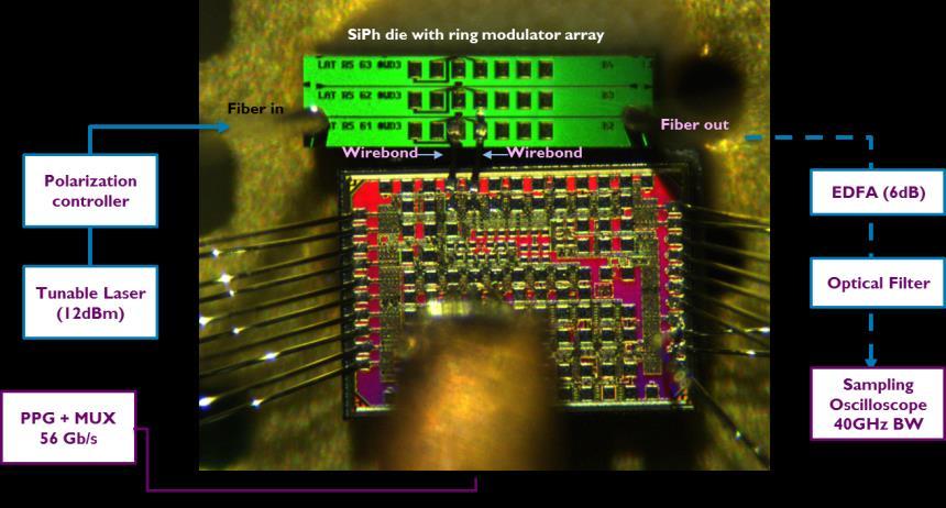
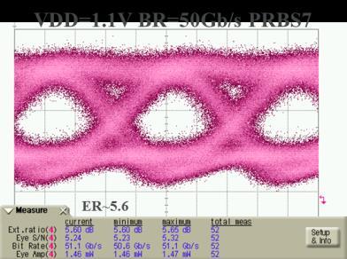
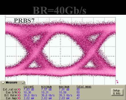
13 IMEC SILICON PHOTONICS TECHNOLOGY Electro-Optical Modulation Options Travelling Wave Mach-Zehnder p-n Modulator 1.5mm 50Gb/s achieved with 2.5V p-p E-O -1V bias ~27GHz V p ~ 11V at quadrature, IL MIN ~ 2.5dB C-Band demonstrated, O-band designs available (similar static performance) 50Gb/s 56Gb/s Ge Electro-Absorption Modulator 50Gb/s achieved with 2.0V p-p (ER ~ 3.0dB, IL ~4.2dB) E-O bias >50GHz Diode capacitance ~ 14fF Both 1615nm & 1560nm operation demonstrated Micro-Ring p-n Modulator 56Gb/s achieved with 1.0V p-p (ER ~ 4.7dB, IL ~3dB) E-O Bandwidth ~47GHz Transmitter 1.5V p-p ~ 11dB C-Band demonstrated, O-band at 40Gb/s Diode capacitance ~20-30fF 56Gb/s

 Device Type I: 0.85 (0.")
 A/W, <50nA, 25GHz Device Type III: 1.15 (0.")
14 IMEC SILICON PHOTONICS TECHNOLOGY Waveguide-Based Ge-on-Si Detectors Options LIGHT 50Gb/s High-speed response limited by reference modulator Typical Performance for TE at -1V, Room T., 1550nm (1310nm) Device Type I: 0.85 (0.88) A/W, <50nA, >50GHz Device Type II: 1.0 (0.94) A/W, <50nA, 25GHz Device Type III: 1.15 (0.86) A/W, <15nA, 15GHz Note: TM characteristics provided in PDK Device Type 2 N = 175 (3 lots, 3 masksets)


15 IMEC SILICON PHOTONICS TECHNOLOGY Fiber Coupling Options Vertical Raised Grating Insertion Loss to SMF-28 <2.5dB (no IMF) Peak-l within-wafer control 1-s <4.0nm 1-dB Bandwidth ~29nm Both C-band & O-band available C-band Edge Coupler Fiber-to-waveguide IL <2dB (High-NA, IMF) Polarization dependent loss <0.5dB Oxide facet 1dB Bandwidth >100nm O-Band designs in characterization


")
16 IMEC SILICON PHOTONICS TECHNOLOGY Passive Waveguide-Based Devices Waveguide Characteristics SWG-WG < 2.0dB/cm, RWG-FC < 1.0dB/cm Thickness Control WG 3-s < 4.5nm Thickness Control FC 3-s < 10nm O-band described in PDK 215nm N=92 wfrs Waveguide-Based Filters Within-device channel spacing control (2.4nm) 3-s < 0.6nm Within-wafer resonator free spectral range (14nm) 3-s < 0.25nm Within-wafer channel wavelength control 3-s < 8.0nm Integrated Heaters Two options: (1) Doped-Si, (2) Tungsten Standard efficiency: P p ~ 17mW High efficiency version: P p ~ 4mW (not MPW compatible) Standard High Efficiency


Multiplexing Filter")


17 IMEC S SILICON PHOTONICS PLATFORM Fully Integrated 8x50G DWDM Si Photonics Technology 56G Silicon Ring Modulator 8+1-channel DWDM (De-)Multiplexing Filter In-Plane Coupler 56Gb/s eye diagram 56G Ge Electro-Absorption Modulator Surface-Normal Coupler 56Gb/s eye diagram 50G Ge Photodetector 50Gb/s eye diagram 56G Silicon Mach-Zehnder Modulator Co-integration of the various building blocks in a single platform Today available on 200mm wafer size, coming soon on 300mm 95% compatible with CMOS130 in commercial foundries

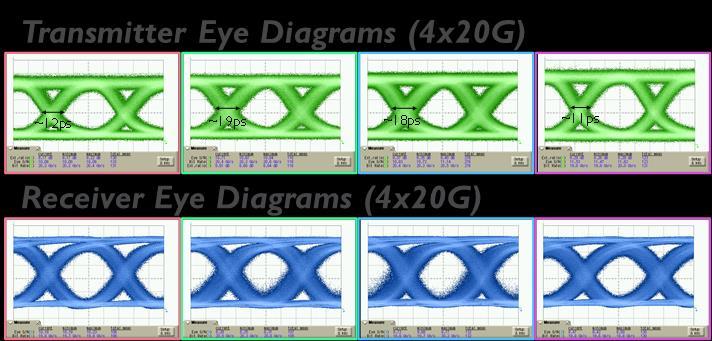

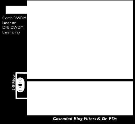
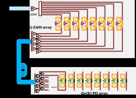
18 HYBRID CMOS SI-PHOTONICS TRANSCEIVER DEMO Putting it all together 40nm CMOS 4x20Gb/s Transceiver 28nm CMOS 50Gb/s Transmitter
 Both MPW and Fully Dedicated Runs Silicon")

19 IMEC S SILICON PHOTONICS OFFERING Build your own Prototype in imec s open platform technology! Accessing imec s 200mm Si Photonics Platform (isipp200) Both MPW and Fully Dedicated Runs Silicon Validated PDK v1.3 is available Supported by various EDA tools >8 Customer tape-outs since 2014, >10 planned in 2016 Interested? Get in touch! MPW Dedicated: Kenneth.Francken@imec.be
20 OUTLINE Introduction Platform Overview Device Library Overview What s Next? Conclusion


21 MONOLITHIC LASERS ON SILICON Addressing extreme cost and performance targets Array of 10 InP lasers under optical pumping Epitaxial growth of III-V Lasers on Silicon InP Silicon Wang, Nature Photonics, October 2015

 (f) TM W=750nm Graphene contact:au/cr Si waveguide Grating coupler + Au/Cr 100μm Graphene Grating coupler Si contact:au/ti 2μm g coupler ct:au/ti")
22 SiO 2 2μm + INTEGRATED GRAPHENE PHOTONICS Au/Cr Addressing extreme cost and performance targets (b) TE W=500nm (c) TM W=750nm 0nm ng coupler + Au/Cr 100μm 0nm Graphene Graphene Photonics Potential for low cost [no SOI, no Ge] Optical devices with wide optical bandwidth Thermally robust modulators 10Gb/s Eye Diagram 10Gb/s eye diagram (d) (a) Grating coupler Si - SiO 2 (e) (b) (d) 50μm Au/Ti n++: cm -3 n+: cm -3 n: cm -3 2μm Grating coupler V 5-nm Thermal oxide W Graphene 0.3μm 2μm TE W=500nm (c) (f) TM W=750nm Graphene contact:au/cr Si waveguide Grating coupler + Au/Cr 100μm Graphene Grating coupler Si contact:au/ti 2μm g coupler ct:au/ti Hu, IEDM μm
23 OUTLINE Introduction Platform Overview Device Library Overview What s Next? Conclusion
24 SUMMARY Scaling the Cloud will require scalable optical interconnects imec s Silicon Photonics Technology offers a scaling path to Terabit/s with >50-Gb/s technology at CMOS-compatible voltages supporting various modulation schemes & wavelength bands considered for future datacenters single-mode interconnects imec is your preferred Silicon Photonics development partner through its prototyping service Silicon Photonics s future... based on non-silicon material
25 ACKNOWLEDGMENTS imec Silicon Photonics R&D team & p-line This work was partially supported by imec s Core Partner Program The research leading to these results has received funding from the European Community's Seventh Framework Programme (FP7/ ) under grant agreement n PLAT4M IMEC
26 THANK YOU!
OPTICAL I/O RESEARCH PROGRAM AT IMEC
 OPTICAL I/O RESEARCH PROGRAM AT IMEC IMEC CORE CMOS PHILIPPE ABSIL, PROGRAM DIRECTOR JORIS VAN CAMPENHOUT, PROGRAM MANAGER SCALING TRENDS IN CHIP-LEVEL I/O RECENT EXAMPLES OF HIGH-BANDWIDTH I/O Graphics
Silicon Photonics Technology Platform To Advance The Development Of Optical Interconnects
 Silicon Photonics Technology Platform To Advance The Development Of Optical Interconnects By Mieke Van Bavel, science editor, imec, Belgium; Joris Van Campenhout, imec, Belgium; Wim Bogaerts, imec s associated
New silicon photonics technology delivers faster data traffic in data centers
 Edition May 2017 Silicon Photonics, Photonics New silicon photonics technology delivers faster data traffic in data centers New transceiver with 10x higher bandwidth than current transceivers. Today, the
Electronic-Photonic ICs for Low Cost and Scalable Datacenter Solutions
 Electronic-Photonic ICs for Low Cost and Scalable Datacenter Solutions Christoph Theiss, Director Packaging Christoph.Theiss@sicoya.com 1 SEMICON Europe 2016, October 27 2016 Sicoya Overview Spin-off from
Lecture: Integration of silicon photonics with electronics. Prepared by Jean-Marc FEDELI CEA-LETI
 Lecture: Integration of silicon photonics with electronics Prepared by Jean-Marc FEDELI CEA-LETI Context The goal is to give optical functionalities to electronics integrated circuit (EIC) The objectives
Integrated Photonics using the POET Optical InterposerTM Platform
 Integrated Photonics using the POET Optical InterposerTM Platform Dr. Suresh Venkatesan CIOE Conference Shenzhen, China Sept. 5, 2018 POET Technologies Inc. TSXV: PUBLIC POET PTK.V Technologies Inc. PUBLIC
Silicon Photonics: an Industrial Perspective
 Silicon Photonics: an Industrial Perspective Antonio Fincato Advanced Programs R&D, Cornaredo, Italy OUTLINE 2 Introduction Silicon Photonics Concept 300mm (12 ) Photonic Process Main Silicon Photonics
EE 232 Lightwave Devices Optical Interconnects
 EE 232 Lightwave Devices Optical Interconnects Sajjad Moazeni Department of Electrical Engineering & Computer Sciences University of California, Berkeley 1 Emergence of Optical Links US IT Map Hyper-Scale
Heinrich-Hertz-Institut Berlin
 NOVEMBER 24-26, ECOLE POLYTECHNIQUE, PALAISEAU OPTICAL COUPLING OF SOI WAVEGUIDES AND III-V PHOTODETECTORS Ludwig Moerl Heinrich-Hertz-Institut Berlin Photonic Components Dept. Institute for Telecommunications,,
An Example Design using the Analog Photonics Component Library. 3/21/2017 Benjamin Moss
 An Example Design using the Analog Photonics Component Library 3/21/2017 Benjamin Moss Component Library Elements Passive Library Elements: Component Current specs 1 Edge Couplers (Si)
A 3.9 ns 8.9 mw 4 4 Silicon Photonic Switch Hybrid-Integrated with CMOS Driver
 A 3.9 ns 8.9 mw 4 4 Silicon Photonic Switch Hybrid-Integrated with CMOS Driver A. Rylyakov, C. Schow, B. Lee, W. Green, J. Van Campenhout, M. Yang, F. Doany, S. Assefa, C. Jahnes, J. Kash, Y. Vlasov IBM
Silicon Photonics Transceivers for Hyper Scale Datacenters: Deployment and Roadmap
 Silicon Photonics Transceivers for Hyper Scale Datacenters: Deployment and Roadmap Peter De Dobbelaere Luxtera Inc. 09/19/2016 Luxtera Proprietary www.luxtera.com Luxtera Company Introduction $100B+ Shift
Si Photonics Technology Platform for High Speed Optical Interconnect. Peter De Dobbelaere 9/17/2012
 Si Photonics Technology Platform for High Speed Optical Interconnect Peter De Dobbelaere 9/17/2012 ECOC 2012 - Luxtera Proprietary www.luxtera.com Overview Luxtera: Introduction Silicon Photonics: Introduction
Si photonics for the Zettabyte Era. Marco Romagnoli. CNIT & TeCIP - Scuola Superiore Sant Anna
 Si photonics for the Zettabyte Era Marco Romagnoli CNIT & TeCIP - Scuola Superiore Sant Anna Semicon 2013 Dresden 8-10 October 2013 Zetabyte era Disaggregation at system level Integration at chip level
APSUNY PDK: Overview and Future Trends
 APSUNY PDK: Overview and Future Trends Erman Timurdogan Analog Photonics, 1 Marina Park Drive, Suite 205, Boston, MA, 02210 erman@analogphotonics.com Silicon Photonics Integrated Circuit Process Design
Silicon Photonics: A Platform for Integration, Wafer Level Assembly and Packaging
 Silicon Photonics: A Platform for Integration, Wafer Level Assembly and Packaging M. Asghari Kotura Inc April 27 Contents: Who is Kotura Choice of waveguide technology Challenges and merits of Si photonics
Si and InP Integration in the HELIOS project
 Si and InP Integration in the HELIOS project J.M. Fedeli CEA-LETI, Grenoble ( France) ECOC 2009 1 Basic information about HELIOS HELIOS photonics ELectronics functional Integration on CMOS www.helios-project.eu
IEEE JOURNAL OF SELECTED TOPICS IN QUANTUM ELECTRONICS 2010 Silicon Photonic Circuits: On-CMOS Integration, Fiber Optical Coupling, and Packaging
 IEEE JOURNAL OF SELECTED TOPICS IN QUANTUM ELECTRONICS 2010 Silicon Photonic Circuits: On-CMOS Integration, Fiber Optical Coupling, and Packaging Christophe Kopp, St ephane Bernab e, Badhise Ben Bakir,
VERSATILE SILICON PHOTONIC PLATFORM FOR DATACOM AND COMPUTERCOM APPLICATIONS. B Szelag CEA-Leti
 VERSATILE SILICON PHOTONIC PLATFORM FOR DATACOM AND COMPUTERCOM APPLICATIONS B Szelag CEA-Leti OUTLINE Silicon photonic : 200mm CMOS core technology towards 300mm Emergent needs vs core process Technological
Opportunities and challenges of silicon photonics based System-In-Package
 Opportunities and challenges of silicon photonics based System-In-Package ECTC 2014 Panel session : Emerging Technologies and Market Trends of Silicon Photonics Speaker : Stéphane Bernabé (Leti Photonics
Silicon Photonics Photo-Detector Announcement. Mario Paniccia Intel Fellow Director, Photonics Technology Lab
 Silicon Photonics Photo-Detector Announcement Mario Paniccia Intel Fellow Director, Photonics Technology Lab Agenda Intel s Silicon Photonics Research 40G Modulator Recap 40G Photodetector Announcement
Silicon photonics with low loss and small polarization dependency. Timo Aalto VTT Technical Research Centre of Finland
 Silicon photonics with low loss and small polarization dependency Timo Aalto VTT Technical Research Centre of Finland EPIC workshop in Tokyo, 9 th November 2017 VTT Technical Research Center of Finland
Silicon Photonics in Optical Communications. Lars Zimmermann, IHP, Frankfurt (Oder), Germany
, Germany") Silicon Photonics in Optical Communications Lars Zimmermann, IHP, Frankfurt (Oder), Germany Outline IHP who we are Silicon photonics Photonic-electronic integration IHP photonic technology Conclusions
Silicon Photonics in Optical Communications Lars Zimmermann, IHP, Frankfurt (Oder), Germany Outline IHP who we are Silicon photonics Photonic-electronic integration IHP photonic technology Conclusions
Convergence Challenges of Photonics with Electronics
 Convergence Challenges of Photonics with Electronics Edward Palen, Ph.D., P.E. PalenSolutions - Optoelectronic Packaging Consulting www.palensolutions.com palensolutions@earthlink.net 415-850-8166 October
CHAPTER 2 POLARIZATION SPLITTER- ROTATOR BASED ON A DOUBLE- ETCHED DIRECTIONAL COUPLER
 CHAPTER 2 POLARIZATION SPLITTER- ROTATOR BASED ON A DOUBLE- ETCHED DIRECTIONAL COUPLER As we discussed in chapter 1, silicon photonics has received much attention in the last decade. The main reason is
New advances in silicon photonics Delphine Marris-Morini
 New advances in silicon photonics Delphine Marris-Morini P. Brindel Alcatel-Lucent Bell Lab, Nozay, France New Advances in silicon photonics D. Marris-Morini, L. Virot*, D. Perez-Galacho, X. Le Roux, D.
Lecture 4 INTEGRATED PHOTONICS
 Lecture 4 INTEGRATED PHOTONICS What is photonics? Photonic applications use the photon in the same way that electronic applications use the electron. Devices that run on light have a number of advantages
Foundry processes for silicon photonics. Pieter Dumon 7 April 2010 ECIO
 Foundry processes for silicon photonics Pieter Dumon 7 April 2010 ECIO Photonics Research Group http://photonics.intec.ugent.be epixfab Prototyping Training Multi project wafer access to silicon photonic
Innovations in Photonic Integration Platforms
 Innovations in Photonic Integration Platforms September 20, 20 Burgeoning Growth Demand Disruptive Technology Video content is fast becoming a larger percentage of total internet traffic 50% Video services
Microphotonics Readiness for Commercial CMOS Manufacturing. Marco Romagnoli
 Microphotonics Readiness for Commercial CMOS Manufacturing Marco Romagnoli MicroPhotonics Consortium meeting MIT, Cambridge October 15 th, 2012 Passive optical structures based on SOI technology Building
Silicon photonics on 3 and 12 μm thick SOI for optical interconnects Timo Aalto VTT Technical Research Centre of Finland
 Silicon photonics on 3 and 12 μm thick SOI for optical interconnects Timo Aalto VTT Technical Research Centre of Finland 5th International Symposium for Optical Interconnect in Data Centres in ECOC, Gothenburg,
New Wave SiP solution for Power
 New Wave SiP solution for Power Vincent Lin Corporate R&D ASE Group APEC March 7 th, 2018 in San Antonio, Texas. 0 Outline Challenges Facing Human Society Energy, Environment and Traffic Autonomous Driving
A tunable Si CMOS photonic multiplexer/de-multiplexer
 A tunable Si CMOS photonic multiplexer/de-multiplexer OPTICS EXPRESS Published : 25 Feb 2010 MinJae Jung M.I.C.S Content 1. Introduction 2. CMOS photonic 1x4 Si ring multiplexer Principle of add/drop filter
Index. Cambridge University Press Silicon Photonics Design Lukas Chrostowski and Michael Hochberg. Index.
 absorption, 69 active tuning, 234 alignment, 394 396 apodization, 164 applications, 7 automated optical probe station, 389 397 avalanche detector, 268 back reflection, 164 band structures, 30 bandwidth
Near/Mid-Infrared Heterogeneous Si Photonics
 PHOTONICS RESEARCH GROUP Near/Mid-Infrared Heterogeneous Si Photonics Zhechao Wang, PhD Photonics Research Group Ghent University / imec, Belgium ICSI-9, Montreal PHOTONICS RESEARCH GROUP 1 Outline Ge-on-Si
IBM T. J. Watson Research Center IBM Corporation
 Broadband Silicon Photonic Switch Integrated with CMOS Drive Electronics B. G. Lee, J. Van Campenhout, A. V. Rylyakov, C. L. Schow, W. M. J. Green, S. Assefa, M. Yang, F. E. Doany, C. V. Jahnes, R. A.
Optical Integrated Devices in Silicon On Insulator for VLSI Photonics
 Optical Integrated Devices in Silicon On Insulator for VLSI Photonics Design, Modelling, Fabrication & Characterization Piero Orlandi 1 Possible Approaches Reduced Design time Transparent Technology Shared
- no emitters/amplifiers available. - complex process - no CMOS-compatible
 Advantages of photonic integrated circuits (PICs) in Microwave Photonics (MWP): compactness low-power consumption, stability flexibility possibility of aggregating optics and electronics functionalities
High-speed Ge photodetector monolithically integrated with large cross silicon-on-insulator waveguide
 [ APPLIED PHYSICS LETTERS ] High-speed Ge photodetector monolithically integrated with large cross silicon-on-insulator waveguide Dazeng Feng, Shirong Liao, Roshanak Shafiiha. etc Contents 1. Introduction
Scalable Electro-optical Assembly Techniques for Silicon Photonics
 Scalable Electro-optical Assembly Techniques for Silicon Photonics Bert Jan Offrein, Tymon Barwicz, Paul Fortier OIDA Workshop on Manufacturing Trends for Integrated Photonics Outline Broadband large channel
A CMOS-compatible silicon photonic platform for high-speed integrated opto-electronics
 Invited Paper A CMOS-compatible silicon photonic platform for high-speed integrated opto-electronics Christophe Galland 1, Ari Novack 3,4, Yang Liu 1, Ran Ding 1, Michael Gould 2, Tom Baehr-Jones 1, Qi
Silicon Optical Modulator
 Silicon Optical Modulator Silicon Optical Photonics Nature Photonics Published online: 30 July 2010 Byung-Min Yu 24 April 2014 High-Speed Circuits & Systems Lab. Dept. of Electrical and Electronic Engineering
Si CMOS Technical Working Group
 Si CMOS Technical Working Group CTR, Spring 2008 meeting Markets Interconnects TWG Breakouts Reception TWG reports Si CMOS: photonic integration E-P synergy - Integration - Standardization - Cross-market
Innovative ultra-broadband ubiquitous Wireless communications through terahertz transceivers ibrow
 Project Overview Innovative ultra-broadband ubiquitous Wireless communications through terahertz transceivers ibrow Mar-2017 Presentation outline Project key facts Motivation Project objectives Project
Optical Bus for Intra and Inter-chip Optical Interconnects
 Optical Bus for Intra and Inter-chip Optical Interconnects Xiaolong Wang Omega Optics Inc., Austin, TX Ray T. Chen University of Texas at Austin, Austin, TX Outline Perspective of Optical Backplane Bus
Overview of short-reach optical interconnects: from VCSELs to silicon nanophotonics
 Acknowledgements: J. Cunningham, R. Ho, X. Zheng, J. Lexau, H. Thacker, J. Yao, Y. Luo, G. Li, I. Shubin, F. Liu, D. Patil, K. Raj, and J. Mitchell M. Asghari T. Pinguet Overview
SILICON PHOTONICS FOR DATA COMMUNICATIONS
 SILICON PHOTONICS FOR DATA COMMUNICATIONS Gideon Yoffe Kaiam Corporation, California Visitor at ICT, KTH Kista Introduction Kaiam packaging technology Data communication, Datacenters Silicon Photonics
Photonic Integrated Circuits Made in Berlin
 Fraunhofer Heinrich Hertz Institute Photonic Integrated Circuits Made in Berlin Photonic integration Workshop, Columbia University, NYC October 2015 Moritz Baier, Francisco M. Soares, Norbert Grote Fraunhofer
Photonics Integration and Evolution of the Optical Transceiver Presented by: Giacomo Losio ProLabs
 Photonics Integration and Evolution of the Optical Transceiver Presented by: Giacomo Losio ProLabs Optical Transceivers architecture is challenged Electrical Driver TIA Laser Photodiode Optical Optical
A Fully Integrated 20 Gb/s Optoelectronic Transceiver Implemented in a Standard
 A Fully Integrated 20 Gb/s Optoelectronic Transceiver Implemented in a Standard 0.13 µm CMOS SOI Technology School of Electrical and Electronic Engineering Yonsei University 이슬아 1. Introduction 2. Architecture
Integrated electro-optical waveguide based devices with liquid crystals on a silicon backplane
 Integrated electro-optical waveguide based devices with liquid crystals on a silicon backplane Florenta Costache Group manager Smart Micro-Optics SMO/AMS Fraunhofer Institute for Photonic Microsystems,
Silicon Photonics Opportunity, applications & Recent Results
 Silicon Photonics Opportunity, applications & Recent Results Dr. Mario Paniccia Intel Fellow Director, Photonics Technology Lab Intel Corporation www.intel.com/go/sp Purdue University Oct 5 2007 Agenda
Silicon Photonics : Towards Heterogeneous and Multi-layer Integration for High Density Circuits
 Silicon Photonics : Towards Heterogeneous and Multi-layer Integration for High Density Circuits Stéphane Bernabé, Ségolène Olivier, Bertrand Szelag, Daivid Fowler, Christophe Kopp OPTICS, Dresden, 23-03-16
Emerging Highly Compact Amplification Solutions for Coherent Transmission
 Emerging Highly Compact Amplification Solutions for Coherent Transmission Market Focus ECOC 2017 Sep 20, 2017 Dr. Sanjai Parthasarathi Vice President, Product Marketing & Strategy II-VI Photonics Outline
Cisco PONC Pavan Voruganti Senior Product Manager. March 2015
 Cisco PONC 2015 Pavan Voruganti Senior Product Manager March 2015 Bandwidth Explosion With a progressive uptake of video, IP, audio and cloud the compound annual growth rate (CAGR) of IP traffic is above
Optical Networks emerging technologies and architectures
 Optical Networks emerging technologies and architectures Faculty of Computer Science, Electronics and Telecommunications Department of Telecommunications Artur Lasoń 100 Gb/s PM-QPSK (DP-QPSK) module Hot
UNIVERSITY OF TORONTO FACULTY OF APPLIED SCIENCE AND ENGINEERING. FINAL EXAMINATION, April 2017 DURATION: 2.5 hours
 UNIVERSITY OF TORONTO FACULTY OF APPLIED SCIENCE AND ENGINEERING ECE4691-111 S - FINAL EXAMINATION, April 2017 DURATION: 2.5 hours Optical Communication and Networks Calculator Type: 2 Exam Type: X Examiner:
Silicon-Organic hybrid Fabrication platform for Integrated circuits FP7-ICT GA No
 www.sofi-ict.eu FP7-ICT-2009.3.8 GA No. 248609 Participants: 2 Outline Today s High Speed Interconnects Vision : Convergence of Photonics & Electronics Silicon Photonics Technology Silicon-Organic Hybrid
Envisioning the Future of Optoelectronic Interconnects:
 Envisioning the Future of Optoelectronic Interconnects: The Production Economics of InP and Si Platforms for 100G Ethernet LAN Transceivers Shan Liu Dr. Erica Fuchs Prof. Randolph Kirchain MIT Microphotonics
Silicon photonics integration roadmap for applications in computing systems
 Silicon photonics integration roadmap for applications in computing systems Bert Jan Offrein Neuromorphic Devices and Systems Group 2016 IBM Corporation Outline Photonics and computing? The interconnect
Silicon Photonics for Mid-Board Optical Modules Marc Epitaux
 Silicon Photonics for Mid-Board Optical Modules Marc Epitaux Chief Architect at Samtec, Inc Outline Interconnect Solutions Mid-Board Optical Modules Silicon Photonics o Benefits o Challenges DragonFly
Photonics and Optical Communication Spring 2005
 Photonics and Optical Communication Spring 2005 Final Exam Instructor: Dr. Dietmar Knipp, Assistant Professor of Electrical Engineering Name: Mat. -Nr.: Guidelines: Duration of the Final Exam: 2 hour You
Numerical Analysis and Optimization of a Multi-Mode Interference Polarization Beam Splitter
 Numerical Analysis and Optimization of a Multi-Mode Interference Polarization Beam Splitter Y. D Mello*, J. Skoric, M. Hui, E. Elfiky, D. Patel, D. Plant Department of Electrical Engineering, McGill University,
Silicon photonics platform for high volume manufacturing. Peter De Dobbelaere Luxtera Inc. 7/11/2018
 Silicon photonics platform for high volume manufacturing Peter De Dobbelaere Luxtera Inc. 7/11/2018 Luxtera Proprietary www.luxtera.com Outline Introduction Silicon Photonics Technology Wafer Process Modules
Silicon-On-Insulator based guided wave optical clock distribution
 Silicon-On-Insulator based guided wave optical clock distribution K. E. Moselund, P. Dainesi, and A. M. Ionescu Electronics Laboratory Swiss Federal Institute of Technology People and funding EPFL Project
Optical Fibers p. 1 Basic Concepts p. 1 Step-Index Fibers p. 2 Graded-Index Fibers p. 4 Design and Fabrication p. 6 Silica Fibers p.
 Preface p. xiii Optical Fibers p. 1 Basic Concepts p. 1 Step-Index Fibers p. 2 Graded-Index Fibers p. 4 Design and Fabrication p. 6 Silica Fibers p. 6 Plastic Optical Fibers p. 9 Microstructure Optical
Silicon Integrated Photonics
 Silicon Integrated Photonics Dr. Mario Paniccia, Director Photonics Technology Lab Intel Corporation IEEE CAS Society May 16, 2005 For More Info http://www.intel.com/technology/silicon/sp/ Intel Corporation
High speed silicon-based optoelectronic devices Delphine Marris-Morini Institut d Electronique Fondamentale, Université Paris Sud
 High speed silicon-based optoelectronic devices Delphine Marris-Morini Institut d Electronique Fondamentale, Université Paris Sud Data centers Optical telecommunications Environment Interconnects Silicon
Monolithic Integra/on of O-band Photonic Transceivers in a Zero-change 32nm SOI CMOS
 Monolithic Integra/on of O-band Photonic Transceivers in a Zero-change 32nm SOI CMOS S. Moazeni 1, A. Atabaki 2, D. Cheian 2, S. Lin 1, R. J. Ram 2, and V. Stojanović 1 1 Department of EECS, University
MODELING AND EVALUATION OF CHIP-TO-CHIP SCALE SILICON PHOTONIC NETWORKS
 1 MODELING AND EVALUATION OF CHIP-TO-CHIP SCALE SILICON PHOTONIC NETWORKS Robert Hendry, Dessislava Nikolova, Sébastien Rumley, Keren Bergman Columbia University HOTI 2014 2 Chip-to-chip optical networks
The Past, Present, and Future of Silicon Photonics
 The Past, Present, and Future of Silicon Photonics Myung-Jae Lee High-Speed Circuits & Systems Lab. Dept. of Electrical and Electronic Engineering Yonsei University Outline Introduction A glance at history
Impact of High-Speed Modulation on the Scalability of Silicon Photonic Interconnects
 Impact of High-Speed Modulation on the Scalability of Silicon Photonic Interconnects OPTICS 201, March 18 th, Dresden, Germany Meisam Bahadori, Sébastien Rumley,and Keren Bergman Lightwave Research Lab,
EPIC: The Convergence of Electronics & Photonics
 EPIC: The Convergence of Electronics & Photonics K-Y Tu, Y.K. Chen, D.M. Gill, M. Rasras, S.S. Patel, A.E. White ell Laboratories, Lucent Technologies M. Grove, D.C. Carothers, A.T. Pomerene, T. Conway
PROJECT FINAL REPORT
 PROJECT FINAL REPORT Grant Agreement number: FP7-224312 Project acronym: HELIOS Project title: photonics ELectronics functional Integration on CMOS Funding Scheme: Large Scale Integrating Project Period
Jan Bogaerts imec
 imec 2007 1 Radiometric Performance Enhancement of APS 3 rd Microelectronic Presentation Days, Estec, March 7-8, 2007 Outline Introduction Backside illuminated APS detector Approach CMOS APS (readout)
Putting PICs in Products A Practical Guideline. Katarzyna Ławniczuk
 Putting PICs in Products A Practical Guideline Katarzyna Ławniczuk k.lawniczuk@brightphotonics.eu Outline Product development considerations Selecting PIC technology Design flow and design tooling considerations
Silicon Photonics and Skorpios Technology Platform. Market Watch ECOC Cannes - September 22, 2014 A. Viglienzoni
 Silicon Photonics and Skorpios Technology Platform Market Watch ECOC Cannes - September 22, 2014 A. Viglienzoni Agenda Preamble Need for Photonics and Integrated Optics Why Current Models Cannot Deliver
Silicon Carrier-Depletion-Based Mach-Zehnder and Ring Modulators with Different Doping Patterns for Telecommunication and Optical Interconnect
 Silicon Carrier-Depletion-Based Mach-Zehnder and Ring Modulators with Different Doping Patterns for Telecommunication and Optical Interconnect Hui Yu, Marianna Pantouvaki*, Joris Van Campenhout*, Katarzyna
Optical Transmission Fundamentals
 Optical Transmission Fundamentals F. Vasey, CERN-EP-ESE Context Technology HEP Specifics 12 Nov 2018 0 Context: Bandwidth Demand Internet traffic is growing at ~Moore s law Global interconnection bandwidth
Graphene electro-optic modulator with 30 GHz bandwidth
 Graphene electro-optic modulator with 30 GHz bandwidth Christopher T. Phare 1, Yoon-Ho Daniel Lee 1, Jaime Cardenas 1, and Michal Lipson 1,2,* 1School of Electrical and Computer Engineering, Cornell University,
Silicon Photonics Opportunity, Applicatoins & Recent Results. Mario Paniccia, Director Photonics Technology Lab Intel Corporation
 Silicon Photonics Opportunity, Applicatoins & Recent Results Mario Paniccia, Director Photonics Technology Lab Intel Corporation Intel Corporation CREOL April 1 2005 Agenda Opportunity for Silicon Photonics
HOW TO CONTINUE COST SCALING. Hans Lebon
 HOW TO CONTINUE COST SCALING Hans Lebon OUTLINE Scaling & Scaling Challenges Imec Technology Roadmap Wafer size scaling : 450 mm 2 COST SCALING IMPROVED PERFORMANCE 3 GLOBAL TRAFFIC FORECAST Cloud Traffic
Heterogeneously Integrated Microwave Signal Generators with Narrow- Linewidth Lasers
 Heterogeneously Integrated Microwave Signal Generators with Narrow- Linewidth Lasers John E. Bowers, Jared Hulme, Tin Komljenovic, Mike Davenport and Chong Zhang Department of Electrical and Computer Engineering
Performance of silicon micro ring modulator with an interleaved p-n junction for optical interconnects
 Indian Journal of Pure & Applied Physics Vol. 55, May 2017, pp. 363-367 Performance of silicon micro ring modulator with an interleaved p-n junction for optical interconnects Priyanka Goyal* & Gurjit Kaur
Optical Communications and Networks - Review and Evolution (OPTI 500) Massoud Karbassian
 Massoud Karbassian") Optical Communications and Networks - Review and Evolution (OPTI 500) Massoud Karbassian m.karbassian@arizona.edu Contents Optical Communications: Review Optical Communications and Photonics Why Photonics?
Optical Communications and Networks - Review and Evolution (OPTI 500) Massoud Karbassian m.karbassian@arizona.edu Contents Optical Communications: Review Optical Communications and Photonics Why Photonics?
Trends in Optical Transceivers:
 Trends in Optical Transceivers: Light sources for premises networks Peter Ronco Corning Optical Fiber Asst. Product Line Manager Premises Fibers January 24, 2006 Outline: Introduction: Transceivers and
Fabrication of High-Speed Resonant Cavity Enhanced Schottky Photodiodes
 Fabrication of High-Speed Resonant Cavity Enhanced Schottky Photodiodes Abstract We report the fabrication and testing of a GaAs-based high-speed resonant cavity enhanced (RCE) Schottky photodiode. The
Laser Systems and Applications
 MSc in Photonics & Europhotonics Laser Systems and Applications Cristina Masoller Research group on Dynamics, Nonlinear Optics and Lasers (DONLL) Departament de Física i Enginyeria Nuclear Universitat
AWG OPTICAL DEMULTIPLEXERS: FROM DESIGN TO CHIP. D. Seyringer
 AWG OPTICAL DEMULTIPLEXERS: FROM DESIGN TO CHIP D. Seyringer Research Centre for Microtechnology, Vorarlberg University of Applied Sciences, Hochschulstr. 1, 6850 Dornbirn, Austria, E-mail: dana.seyringer@fhv.at
Challenges for On-chip Optical Interconnect
 Initial Results of Prototyping a 3-D Integrated Intra-Chip Free-Space Optical Interconnect Berkehan Ciftcioglu, Rebecca Berman, Jian Zhang, Zach Darling, Alok Garg, Jianyun Hu, Manish Jain, Peng Liu, Ioannis
MICRO RING MODULATOR. Dae-hyun Kwon. High-speed circuits and Systems Laboratory
 MICRO RING MODULATOR Dae-hyun Kwon High-speed circuits and Systems Laboratory Paper preview Title of the paper Low Vpp, ultralow-energy, compact, high-speed silicon electro-optic modulator Publication
D10.08 Project publishable summary PROJECT PUBLISHABLE SUMMARY D10.08
 PROJECT PUBLISHABLE SUMMARY D10.08 Grant Agreement number: FP7-318178 Project acronym: PLAT4M Project title: Photonic Libraries And Technology for Manufacturing Funding Scheme: Large Scale Integrating
GoToWebinar Housekeeping: attendee screen Lumerical Solutions, Inc.
 GoToWebinar Housekeeping: attendee screen 2012 Lumerical Solutions, Inc. GoToWebinar Housekeeping: your participation Open and hide your control panel Join audio: Choose Mic & Speakers to use VoIP Choose
The Light at the End of the Wire. Dana Vantrease + HP Labs + Mikko Lipasti
 The Light at the End of the Wire Dana Vantrease + HP Labs + Mikko Lipasti 1 Goals of This Talk Why should we (architects) be interested in optics? How does on-chip optics work? What can we build with optics?
inemi OPTOELECTRONICS ROADMAP FOR 2004 Dr. Laura J. Turbini University of Toronto SMTA International September 26, 2005
 inemi OPTOELECTRONICS ROADMAP FOR 2004 0 Dr. Laura J. Turbini University of Toronto SMTA International September 26, 2005 Outline Business Overview Traditional vs Jisso Packaging Levels Optoelectronics
Integration of Optoelectronic and RF Devices for Applications in Optical Interconnect and Wireless Communication
 Integration of Optoelectronic and RF Devices for Applications in Optical Interconnect and Wireless Communication Zhaoran (Rena) Huang Assistant Professor Department of Electrical, Computer and System Engineering
160-Gb/s Bidirectional Parallel Optical Transceiver Module for Board-Level Interconnects
 160-Gb/s Bidirectional Parallel Optical Transceiver Module for Board-Level Interconnects Fuad Doany, Clint Schow, Jeff Kash C. Baks, D. Kuchta, L. Schares, & R. John IBM T. J. Watson Research Center doany@us.ibm.com
Photonic modules for data centers Leti SAMTEC FINAL p Photonic modules for data centers require cutting edge technologies
 Photonic modules for data centers Leti SAMTEC FINAL p. 1 072817 Photonic modules for data centers require cutting edge technologies by Stéphane Bernabé, Olivier Castany, Bertrand Szelag, Benoît Charbonnier
CHAPTER 4 RESULTS. 4.1 Introduction
 CHAPTER 4 RESULTS 4.1 Introduction In this chapter focus are given more on WDM system. The results which are obtained mainly from the simulation work are presented. In simulation analysis, the study will
Multi-gigabit intra-satellite interconnects employing multi-core fibers and optical engines
 VTT TECHNICAL RESEARCH CENTRE OF FINLAND LTD at ICSO conference 19 Oct 2016 Multi-gigabit intra-satellite interconnects employing multi-core fibers and optical engines Mikko Karppinen et al. VTT P. Westbergh,