Silicon-On-Insulator based guided wave optical clock distribution
|
|
|
- Jason Anderson
- 6 years ago
- Views:
Transcription


1 Silicon-On-Insulator based guided wave optical clock distribution K. E. Moselund, P. Dainesi, and A. M. Ionescu Electronics Laboratory Swiss Federal Institute of Technology
2 People and funding EPFL Project leader: Prof. Adrian M. Ionescu Post. Doc: Dr. Paolo Dainesi Ph.D. student: Kirsten E. Moselund Visiting academic host: Rodica Plugaru External partner: ST Microelectronics Thomas Skotnicki, Philippe Coronel, Matthieu Bopp (Ph.D.) Funding: Integrated Systems Center, EPFL.
3 Overview Introduction Optical interconnect Components for Optical Signaling Silicon based light sources Waveguiding Optical Modulator Different approaches GAA optical phase modulator Simulation GAA MOSFET at EPFL Intensity modulator SiGe based light detection Conclusion
4 Trends in Microelectronics Increase of complexity and functionality Transistors get smaller and faster. Clock signal frequency is raised. Interconnection cross section is squeezed. Interconnection length can become even longer. Some possible proposed classical solutions Line equalization. Use of repeater amplifier (on chip only) but with power and complexity penalty. On chip asynchronous networking (AMD 64). Our approach On-chip optical interconnect


5 Bandwidth and delay Electrical interconnect Electrical interconnect RC time constant does not scale with the technology, but remain constant. Synchronous clock distribution is problematic. New generations will face the RC-LC behavior boundary. ITRS 2003 ITRS 2003 Performance dominated by interconnects. Optical interconnect a solution? - critical length above which optical system is faster than electrical = a few mm. P. Kapur et al. 2002

6 Potentials On chip guided wave optical clock distribution Inherently synchronous for wafer-scale dimensions. Design does not need to be reconsidered for a change in modulation frequency. Immune to electromagnetic interference with adjacent electronics or RF signals. WDM and TDM are possible. Limitations Difficult to implement light sources, waveguide and detectors in the same substrate? High propagation and coupling loss. Challenges with regards to layout and process development. Dispersion may become relevant for long waveguides. Power still an issue, K. especially Moselund CSI for Seminar short Oct. links 25th (receiver dominated).

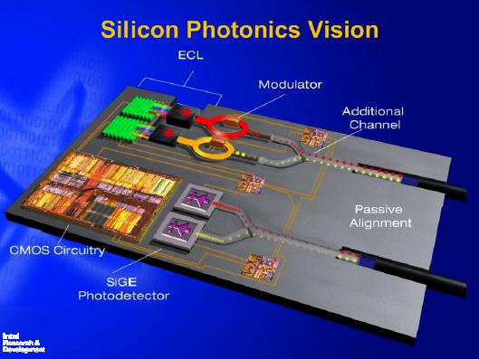
7 Building blocks of a photonic IC
8

.")
9 Components for on-chip optical signaling Waveguiding Low propagation losses (<1dB/cm). Low bending losses and small band radii Small waveguides with high Dn. Compact and low loss coupling devices. Waveguide dimension compatible with electronics size scale. Detection Monolithically integrated. Small size and low power. High efficiency. High speed. Clock source External: Low loss, high efficiency coupling (mode size converter or grating). Internal: Monolithically or hybrid light source and GHz rate modulator. SOI photonic wire SiGe detector External laser + modulator
10 Light Source
11 Wavelength Telecom: Short haul 850nm Long Haul um On-chip signaling: Visible Si for detection, and polymers for waveguiding. IR (>1.1um) Si is ideal for waveguiding, but requires more advanced detection scheme (SiGe, III-V s). Monolithic integration on the Si-chip
 Larger bandgap Greater excitation efficiency of rare earth ions. Quantum efficiencies (LED) ~20%.")
12 Silicon Light-Emitting Diode Structure Silicon Rich Oxide (SRO) doped with rareearth ions. SRO is SiO2 enriched with Si-nanocrystals. Sandwiched between n+ poly-si and p+ Si. Small size of nanocrystals (1-2nm) Larger bandgap Greater excitation efficiency of rare earth ions. Quantum efficiencies (LED) ~20%.

13 Si-based light sources Raman amplification: Pump photon absorbed emission of signal photon (lower energy) + a phonon. Small effect need high pump intensity + very low absorption. Two-photon absorption: Creates electron/hole pairs, which absorb both pump and signal light. Turns off laser light. Unwanted effect! J. Faist, Nature 2005.

14 CW Silicon Raman Laser Rong et al. Nature 2005 SOI technology Tight confinement. Optical pump intensity = 25MWcm -2. Reverse-bias PiN diode removes electrons and holes from the waveguide. Continuous operation.
15 Waveguiding
16 Waveguiding - requirements Waveguiding Low propagation losses (<1dB/cm). Since optical signaling is only advantageous for global signals. Low bending losses and small band radii. Small waveguides with high Dn. Compact and low loss coupling devices. For splitters and/or multiplexers. Low-loss input/output coupling. Waveguide dimensions compatible with electronics size scale. Compatible with CMOS processing. Good control of material and surface quality. Scattering is the most important loss mechanism for nanowires.
17 Free space External light source broadcasted to different photodetectors. Issues: Holographic element required. Photogeneration outside PD area. Complicated, bulky(3d) and fragile. Guided wave External or internal light sources. Issues: Propagation losses. Bend losses. Light coupling (for external source). On chip clock distribution

 Good confinement very compact devices and small (2-5mm) radius bends.")
18 Guided wave approach Polymer waveguide Visible region. Si as photodetector. Small Dn low confinement Large Devices Photonic wire Rib waveguide H = W ~ 1-2mm Modest coupling efficiency with optical fibers. Moderate confinement moderately long devices IR region (>1.1um) Good confinement very compact devices and small (2-5mm) radius bends. Very Low coupling efficiency requires coupling structure. Fraction of light travels outside the physical guide surface roughness is very important.
 +")

 Roughness reduction. Reduction of lateral dimensions.")
19 Sub-mm SOI Waveguides Illustration Process steps SOI P-type substrate: BOX=1mm, SOI Si=340nm Hard mask 20nm SiO2 (thermal) + 50nm Si3N4 Lithography Resist: S1805, 0.5um, Laser direct writing Resolution: 0.8mm Etch hard mask Etch waveguides Oxidation ( nm much less due to stress) Roughness reduction. Reduction of lateral dimensions. Deep etch Define waveguide and chip dimension (end coupling). Chip Dicing
 SOI waveguides on Si-chip, size limited by lithographic resolution.")

20 Characterization? Nanoscale (0.3x0.8um) SOI waveguides on Si-chip, size limited by lithographic resolution. Deep etch in order to approach fiber to the guide (end coupling). 1. Substrate coupling, due to large size of fibre compared to guide. 2. missing corners at taper level, the origin of which is not established. 3. Currently working on the implementation of a polymer taper by spray-coating.


21 Polymer taper Spraycoating of polymer: Polymer taper as the last step before dicing. Technologically simple. Allows for high aspect ratio polymer deposition spin coating is not possible. Problems Adhesion of polymer. Uneven coating close to edge. Roughness of polymer layer. IR losses in the polymer.


22 Suspended Nanowires Rough waveguides Taper delamination Suspended waveguides Single-crystal Si waveguides on bulk Si. Smooth sidewalls due to oxidation. Anchors required during processing.

23 Characteristics Cleaved waveguide, surrounded by 200nm oxide and air. Dimensions ~630nm x 380nm. Characteristics Triangular or rectangular cross section. Dimensions from 1um down to a few 100nm. Surrounded by air or oxide Taper at end ~0.4x1um. Problems Light coupling has been unsuccessful so far. Polymer taper is not readily implemented. Possible polymer deposition at input, due to deep etch process. Very fragile during CMP.
24 Light Modulator (CSI funded project)


25 Optical phase modulator previous work Functionality Modulation of refractive index by free carrier injection phase modulation of propagating light. P. Dainesi et al. Photon. Tech. Lett M. mazza et al. Transducers PiN - diode based High modulation efficiency VpL= 0.2 Vcm. Low speed limited by recombination -100 s MHz. Current injection heating. Schottky diode based Potentially faster than PiN, but still limited by recombination. Work in progress by R. Plugaru and M. Mazza
 2004 MOS Capacitive Operation High speed (1GHz achieved).")

26 Optical phase modulator capacitive operation A. Liu et al. Nature 427 (6975) 2004 MOS Capacitive Operation High speed (1GHz achieved). Low efficiency VpL= 10 Vcm Negligible static power consumption. Novel GAA MOS modulator Si-core, gate oxide and Poly serves as waveguide. High efficiency VpL= 0.47 Vcm (ideal). High loss ~30dB/cm. K. Moselund et al. Transducers K Moselund CSI Seminar Oct. 25th


27 Gate-All-Around Phase Modulator GAA optical modulator Operation mode: accumulation or inversion. Creation of thin charge region at both sides of the interface. No problem with corner effect turned into a positive effect.

28 Optimum dimensions Shrinking of core dimension The fraction of light confined to the modulated region is reduced. The average modulation in the core is increased. There exists an optimum dimension with respect to efficiency

29 Transient performance Switching speeds in the 10s of GHZ (device only). High Doping High speed, but also high loss. Speed proportional to source-drain distance a series connection K. Moselund of several CSI Seminar shorter Oct. 25th devices is required.
 Compact.")
 \" cav = 30dB/cm \" cav = 100dB/cm!\" si-core = 9dB/cm 0.0 1.548 1.550 1.")
30 Intensity modulator Mach-Zender interferometer. Easy to implement. Large (p-phase shift). Intensity modulator Fabry-Perot resonator Resonant structures Small phase shift required (value depends on finesse) Compact. Very sensitive to optical loss difficult to design. Normalized transmission R = 87.8% T = 11.9% " scat = 0.3% L cav = 80#/2n OFF state " cav = 0 (ideal) " cav = 30dB/cm " cav = 100dB/cm!" si-core = 9dB/cm Wavelength (µm) ON state P. Dainesi et al. CLEO 2005
, 2004 V. R.")


31 Micro Ring resonator R. Baets et al., PTL 16 (5), 2004 V. R. Almeida et al. Nature S. Pradhan et al. CLEO 2005 Micro ring resonator No need for Bragg gratings. Good control of gap required. Vertical implementation is possible. Active functionality using a PiN diode has been implemented.

32 Implementation based on utility Low doping NA = ND = Modulation depth = 91% Loss = 3 db Max. frequency = 38 GHz Modulation depth = 91% Loss = 1.5 db Max. frequency = 38 GHz Low Loss! High doping NA = ND = Modulation depth = 85% Loss = 6 db Max. frequency = 80 GHz High Speed! Modulation depth = 85% Loss = 4.5 db Max. frequency = 80 GHz P. Dainesi et al. CLEO 2005
33 Short term goals (1 year) Experimental validation of new GAA MOSFET. different architecture for light propagation, compared to previously fabricated GAA at CMI. Finalization of suspended wire fabrication technology. Surface roughness, anchor dimensions. Experimental validation of light modulation based on the suspended nanowire approach. No resonant cavity in this technology! Enhanced modeling of GAA light modulator device based on experimental data.
34 Light detection
.")
35 SiGe Detectors Ge absorbs in the IR. SiGe detectors SiGe already used in CMOS technology (mobility enhancement). 4% lattice mismatch between Si and Ge strain, dislocations. H. Presting 1998
36 Conclusion Optical interconnects is a possible candidate for future on-chip global signal distribution. Capacitive modulation in a MOS structure is extremely fast and with low power consumption. Using a GAA in a resonant cavity approach it should be possible to combine both high efficiency and high speed operation. Light coupling into sub-mm structures is extremely difficult, and a solution to this problem must be found. Efficient light emission and detection are still critical issues, but not prohibitive.
Lecture 4 INTEGRATED PHOTONICS
 Lecture 4 INTEGRATED PHOTONICS What is photonics? Photonic applications use the photon in the same way that electronic applications use the electron. Devices that run on light have a number of advantages
Lecture: Integration of silicon photonics with electronics. Prepared by Jean-Marc FEDELI CEA-LETI
 Lecture: Integration of silicon photonics with electronics Prepared by Jean-Marc FEDELI CEA-LETI Context The goal is to give optical functionalities to electronics integrated circuit (EIC) The objectives
Index. Cambridge University Press Silicon Photonics Design Lukas Chrostowski and Michael Hochberg. Index.
 absorption, 69 active tuning, 234 alignment, 394 396 apodization, 164 applications, 7 automated optical probe station, 389 397 avalanche detector, 268 back reflection, 164 band structures, 30 bandwidth
Silicon Photonics Photo-Detector Announcement. Mario Paniccia Intel Fellow Director, Photonics Technology Lab
 Silicon Photonics Photo-Detector Announcement Mario Paniccia Intel Fellow Director, Photonics Technology Lab Agenda Intel s Silicon Photonics Research 40G Modulator Recap 40G Photodetector Announcement
NEXT GENERATION SILICON PHOTONICS FOR COMPUTING AND COMMUNICATION PHILIPPE ABSIL
 NEXT GENERATION SILICON PHOTONICS FOR COMPUTING AND COMMUNICATION PHILIPPE ABSIL OUTLINE Introduction Platform Overview Device Library Overview What s Next? Conclusion OUTLINE Introduction Platform Overview
A continuous-wave Raman silicon laser
 A continuous-wave Raman silicon laser Haisheng Rong, Richard Jones,.. - Intel Corporation Ultrafast Terahertz nanoelectronics Lab Jae-seok Kim 1 Contents 1. Abstract 2. Background I. Raman scattering II.
Si CMOS Technical Working Group
 Si CMOS Technical Working Group CTR, Spring 2008 meeting Markets Interconnects TWG Breakouts Reception TWG reports Si CMOS: photonic integration E-P synergy - Integration - Standardization - Cross-market
Photonic Integrated Circuits Made in Berlin
 Fraunhofer Heinrich Hertz Institute Photonic Integrated Circuits Made in Berlin Photonic integration Workshop, Columbia University, NYC October 2015 Moritz Baier, Francisco M. Soares, Norbert Grote Fraunhofer
High speed silicon-based optoelectronic devices Delphine Marris-Morini Institut d Electronique Fondamentale, Université Paris Sud
 High speed silicon-based optoelectronic devices Delphine Marris-Morini Institut d Electronique Fondamentale, Université Paris Sud Data centers Optical telecommunications Environment Interconnects Silicon
Electronic-Photonic ICs for Low Cost and Scalable Datacenter Solutions
 Electronic-Photonic ICs for Low Cost and Scalable Datacenter Solutions Christoph Theiss, Director Packaging Christoph.Theiss@sicoya.com 1 SEMICON Europe 2016, October 27 2016 Sicoya Overview Spin-off from
Semiconductor Optical Communication Components and Devices Lecture 18: Introduction to Diode Lasers - I
 Semiconductor Optical Communication Components and Devices Lecture 18: Introduction to Diode Lasers - I Prof. Utpal Das Professor, Department of lectrical ngineering, Laser Technology Program, Indian Institute
Micro-sensors - what happens when you make "classical" devices "small": MEMS devices and integrated bolometric IR detectors
 Micro-sensors - what happens when you make "classical" devices "small": MEMS devices and integrated bolometric IR detectors Dean P. Neikirk 1 MURI bio-ir sensors kick-off 6/16/98 Where are the targets
New advances in silicon photonics Delphine Marris-Morini
 New advances in silicon photonics Delphine Marris-Morini P. Brindel Alcatel-Lucent Bell Lab, Nozay, France New Advances in silicon photonics D. Marris-Morini, L. Virot*, D. Perez-Galacho, X. Le Roux, D.
Robert G. Hunsperger. Integrated Optics. Theory and Technology. Sixth Edition. 4ü Spri rineer g<
 Robert G. Hunsperger Integrated Optics Theory and Technology Sixth Edition 4ü Spri rineer g< 1 Introduction 1 1.1 Advantages of Integrated Optics 2 1.1.1 Comparison of Optical Fibers with Other Interconnectors
Alternatives to standard MOSFETs. What problems are we really trying to solve?
 Alternatives to standard MOSFETs A number of alternative FET schemes have been proposed, with an eye toward scaling up to the 10 nm node. Modifications to the standard MOSFET include: Silicon-in-insulator
A 3.9 ns 8.9 mw 4 4 Silicon Photonic Switch Hybrid-Integrated with CMOS Driver
 A 3.9 ns 8.9 mw 4 4 Silicon Photonic Switch Hybrid-Integrated with CMOS Driver A. Rylyakov, C. Schow, B. Lee, W. Green, J. Van Campenhout, M. Yang, F. Doany, S. Assefa, C. Jahnes, J. Kash, Y. Vlasov IBM
Lecture 6 Fiber Optical Communication Lecture 6, Slide 1
 Lecture 6 Optical transmitters Photon processes in light matter interaction Lasers Lasing conditions The rate equations CW operation Modulation response Noise Light emitting diodes (LED) Power Modulation
Basic concepts. Optical Sources (b) Optical Sources (a) Requirements for light sources (b) Requirements for light sources (a)
 Optical Sources (a) Requirements for light sources (b) Requirements for light sources (a)") Optical Sources (a) Optical Sources (b) The main light sources used with fibre optic systems are: Light-emitting diodes (LEDs) Semiconductor lasers (diode lasers) Fibre laser and other compact solid-state
Optical Sources (a) Optical Sources (b) The main light sources used with fibre optic systems are: Light-emitting diodes (LEDs) Semiconductor lasers (diode lasers) Fibre laser and other compact solid-state
Silicon Photonics Opportunity, applications & Recent Results
 Silicon Photonics Opportunity, applications & Recent Results Dr. Mario Paniccia Intel Fellow Director, Photonics Technology Lab Intel Corporation www.intel.com/go/sp Purdue University Oct 5 2007 Agenda
Silicon Photonics: A Platform for Integration, Wafer Level Assembly and Packaging
 Silicon Photonics: A Platform for Integration, Wafer Level Assembly and Packaging M. Asghari Kotura Inc April 27 Contents: Who is Kotura Choice of waveguide technology Challenges and merits of Si photonics
IEEE JOURNAL OF SELECTED TOPICS IN QUANTUM ELECTRONICS 2010 Silicon Photonic Circuits: On-CMOS Integration, Fiber Optical Coupling, and Packaging
 IEEE JOURNAL OF SELECTED TOPICS IN QUANTUM ELECTRONICS 2010 Silicon Photonic Circuits: On-CMOS Integration, Fiber Optical Coupling, and Packaging Christophe Kopp, St ephane Bernab e, Badhise Ben Bakir,
Convergence Challenges of Photonics with Electronics
 Convergence Challenges of Photonics with Electronics Edward Palen, Ph.D., P.E. PalenSolutions - Optoelectronic Packaging Consulting www.palensolutions.com palensolutions@earthlink.net 415-850-8166 October
Chapter 8. Wavelength-Division Multiplexing (WDM) Part II: Amplifiers
 Part II: Amplifiers") Chapter 8 Wavelength-Division Multiplexing (WDM) Part II: Amplifiers Introduction Traditionally, when setting up an optical link, one formulates a power budget and adds repeaters when the path loss exceeds
Chapter 8 Wavelength-Division Multiplexing (WDM) Part II: Amplifiers Introduction Traditionally, when setting up an optical link, one formulates a power budget and adds repeaters when the path loss exceeds
Optical Fibers p. 1 Basic Concepts p. 1 Step-Index Fibers p. 2 Graded-Index Fibers p. 4 Design and Fabrication p. 6 Silica Fibers p.
 Preface p. xiii Optical Fibers p. 1 Basic Concepts p. 1 Step-Index Fibers p. 2 Graded-Index Fibers p. 4 Design and Fabrication p. 6 Silica Fibers p. 6 Plastic Optical Fibers p. 9 Microstructure Optical
Silicon Photonics Technology Platform To Advance The Development Of Optical Interconnects
 Silicon Photonics Technology Platform To Advance The Development Of Optical Interconnects By Mieke Van Bavel, science editor, imec, Belgium; Joris Van Campenhout, imec, Belgium; Wim Bogaerts, imec s associated
Innovative ultra-broadband ubiquitous Wireless communications through terahertz transceivers ibrow
 Project Overview Innovative ultra-broadband ubiquitous Wireless communications through terahertz transceivers ibrow Mar-2017 Presentation outline Project key facts Motivation Project objectives Project
A Fully Integrated 20 Gb/s Optoelectronic Transceiver Implemented in a Standard
 A Fully Integrated 20 Gb/s Optoelectronic Transceiver Implemented in a Standard 0.13 µm CMOS SOI Technology School of Electrical and Electronic Engineering Yonsei University 이슬아 1. Introduction 2. Architecture
Introduction Fundamentals of laser Types of lasers Semiconductor lasers
 ECE 5368 Introduction Fundamentals of laser Types of lasers Semiconductor lasers Introduction Fundamentals of laser Types of lasers Semiconductor lasers How many types of lasers? Many many depending on
Session 2: Silicon and Carbon Photonics (11:00 11:30, Huxley LT311)
") Session 2: Silicon and Carbon Photonics (11:00 11:30, Huxley LT311) (invited) Formation and control of silicon nanocrystals by ion-beams for photonic applications M Halsall The University of Manchester,
Session 2: Silicon and Carbon Photonics (11:00 11:30, Huxley LT311) (invited) Formation and control of silicon nanocrystals by ion-beams for photonic applications M Halsall The University of Manchester,
Fabrication of High-Speed Resonant Cavity Enhanced Schottky Photodiodes
 Fabrication of High-Speed Resonant Cavity Enhanced Schottky Photodiodes Abstract We report the fabrication and testing of a GaAs-based high-speed resonant cavity enhanced (RCE) Schottky photodiode. The
Optodevice Data Book ODE I. Rev.9 Mar Opnext Japan, Inc.
 Optodevice Data Book ODE-408-001I Rev.9 Mar. 2003 Opnext Japan, Inc. Section 1 Operating Principles 1.1 Operating Principles of Laser Diodes (LDs) and Infrared Emitting Diodes (IREDs) 1.1.1 Emitting Principles
On-chip Si-based Bragg cladding waveguide with high index contrast bilayers
 On-chip Si-based Bragg cladding waveguide with high index contrast bilayers Yasha Yi, Shoji Akiyama, Peter Bermel, Xiaoman Duan, and L. C. Kimerling Massachusetts Institute of Technology, 77 Massachusetts
Silicon Photonics in Optical Communications. Lars Zimmermann, IHP, Frankfurt (Oder), Germany
, Germany") Silicon Photonics in Optical Communications Lars Zimmermann, IHP, Frankfurt (Oder), Germany Outline IHP who we are Silicon photonics Photonic-electronic integration IHP photonic technology Conclusions
Silicon Photonics in Optical Communications Lars Zimmermann, IHP, Frankfurt (Oder), Germany Outline IHP who we are Silicon photonics Photonic-electronic integration IHP photonic technology Conclusions
Lecture 9 External Modulators and Detectors
 Optical Fibres and Telecommunications Lecture 9 External Modulators and Detectors Introduction Where are we? A look at some real laser diodes. External modulators Mach-Zender Electro-absorption modulators
High-speed Ge photodetector monolithically integrated with large cross silicon-on-insulator waveguide
 [ APPLIED PHYSICS LETTERS ] High-speed Ge photodetector monolithically integrated with large cross silicon-on-insulator waveguide Dazeng Feng, Shirong Liao, Roshanak Shafiiha. etc Contents 1. Introduction
The Past, Present, and Future of Silicon Photonics
 The Past, Present, and Future of Silicon Photonics Myung-Jae Lee High-Speed Circuits & Systems Lab. Dept. of Electrical and Electronic Engineering Yonsei University Outline Introduction A glance at history
Silicon Photonics: an Industrial Perspective
 Silicon Photonics: an Industrial Perspective Antonio Fincato Advanced Programs R&D, Cornaredo, Italy OUTLINE 2 Introduction Silicon Photonics Concept 300mm (12 ) Photonic Process Main Silicon Photonics
Optical Amplifiers Photonics and Integrated Optics (ELEC-E3240) Zhipei Sun Photonics Group Department of Micro- and Nanosciences Aalto University
 Zhipei Sun Photonics Group Department of Micro- and Nanosciences Aalto University") Photonics Group Department of Micro- and Nanosciences Aalto University Optical Amplifiers Photonics and Integrated Optics (ELEC-E3240) Zhipei Sun Last Lecture Topics Course introduction Ray optics & optical
Photonics Group Department of Micro- and Nanosciences Aalto University Optical Amplifiers Photonics and Integrated Optics (ELEC-E3240) Zhipei Sun Last Lecture Topics Course introduction Ray optics & optical
Near/Mid-Infrared Heterogeneous Si Photonics
 PHOTONICS RESEARCH GROUP Near/Mid-Infrared Heterogeneous Si Photonics Zhechao Wang, PhD Photonics Research Group Ghent University / imec, Belgium ICSI-9, Montreal PHOTONICS RESEARCH GROUP 1 Outline Ge-on-Si
Integrated photonic circuit in silicon on insulator for Fourier domain optical coherence tomography
 Integrated photonic circuit in silicon on insulator for Fourier domain optical coherence tomography Günay Yurtsever *,a, Pieter Dumon a, Wim Bogaerts a, Roel Baets a a Ghent University IMEC, Photonics
Optics Communications
 Optics Communications 283 (2010) 3678 3682 Contents lists available at ScienceDirect Optics Communications journal homepage: www.elsevier.com/locate/optcom Ultra-low-loss inverted taper coupler for silicon-on-insulator
Figure 1 Basic waveguide structure
 Recent Progress in SOI Nanophotonic Waveguides D. Van Thourhout, P. Dumon, W. Bogaerts, G. Roelkens, D. Taillaert, G. Priem, R. Baets IMEC-Ghent University, Department of Information Technology, St. Pietersnieuwstraat
Si and InP Integration in the HELIOS project
 Si and InP Integration in the HELIOS project J.M. Fedeli CEA-LETI, Grenoble ( France) ECOC 2009 1 Basic information about HELIOS HELIOS photonics ELectronics functional Integration on CMOS www.helios-project.eu
Heinrich-Hertz-Institut Berlin
 NOVEMBER 24-26, ECOLE POLYTECHNIQUE, PALAISEAU OPTICAL COUPLING OF SOI WAVEGUIDES AND III-V PHOTODETECTORS Ludwig Moerl Heinrich-Hertz-Institut Berlin Photonic Components Dept. Institute for Telecommunications,,
A thin foil optical strain gage based on silicon-on-insulator microresonators
 A thin foil optical strain gage based on silicon-on-insulator microresonators D. Taillaert* a, W. Van Paepegem b, J. Vlekken c, R. Baets a a Photonics research group, Ghent University - INTEC, St-Pietersnieuwstraat
Nanophotonics for low latency optical integrated circuits
 Nanophotonics for low latency optical integrated circuits Akihiko Shinya NTT Basic Research Labs., Nanophotonics Center, NTT Corporation MPSoC 17, Annecy, France Outline Low latency optical circuit BDD
Optical Interconnection in Silicon LSI
 The Fifth Workshop on Nanoelectronics for Tera-bit Information Processing, 1 st Century COE, Hiroshima University Optical Interconnection in Silicon LSI Shin Yokoyama, Yuichiro Tanushi, and Masato Suzuki
Silicon Carrier-Depletion-Based Mach-Zehnder and Ring Modulators with Different Doping Patterns for Telecommunication and Optical Interconnect
 Silicon Carrier-Depletion-Based Mach-Zehnder and Ring Modulators with Different Doping Patterns for Telecommunication and Optical Interconnect Hui Yu, Marianna Pantouvaki*, Joris Van Campenhout*, Katarzyna
White Paper Laser Sources For Optical Transceivers. Giacomo Losio ProLabs Head of Technology
 White Paper Laser Sources For Optical Transceivers Giacomo Losio ProLabs Head of Technology September 2014 Laser Sources For Optical Transceivers Optical transceivers use different semiconductor laser
Optical Transmission Fundamentals
 Optical Transmission Fundamentals F. Vasey, CERN-EP-ESE Context Technology HEP Specifics 12 Nov 2018 0 Context: Bandwidth Demand Internet traffic is growing at ~Moore s law Global interconnection bandwidth
Waveguiding in PMMA photonic crystals
 ROMANIAN JOURNAL OF INFORMATION SCIENCE AND TECHNOLOGY Volume 12, Number 3, 2009, 308 316 Waveguiding in PMMA photonic crystals Daniela DRAGOMAN 1, Adrian DINESCU 2, Raluca MÜLLER2, Cristian KUSKO 2, Alex.
CMOS Digital Integrated Circuits Lec 2 Fabrication of MOSFETs
 CMOS Digital Integrated Circuits Lec 2 Fabrication of MOSFETs 1 CMOS Digital Integrated Circuits 3 rd Edition Categories of Materials Materials can be categorized into three main groups regarding their
A new picosecond Laser pulse generation method.
 PULSE GATING : A new picosecond Laser pulse generation method. Picosecond lasers can be found in many fields of applications from research to industry. These lasers are very common in bio-photonics, non-linear
MICRO RING MODULATOR. Dae-hyun Kwon. High-speed circuits and Systems Laboratory
 MICRO RING MODULATOR Dae-hyun Kwon High-speed circuits and Systems Laboratory Paper preview Title of the paper Low Vpp, ultralow-energy, compact, high-speed silicon electro-optic modulator Publication
Optical MEMS in Compound Semiconductors Advanced Engineering Materials, Cal Poly, SLO November 16, 2007
 Optical MEMS in Compound Semiconductors Advanced Engineering Materials, Cal Poly, SLO November 16, 2007 Outline Brief Motivation Optical Processes in Semiconductors Reflectors and Optical Cavities Diode
Review of Semiconductor Physics
 Review of Semiconductor Physics k B 1.38 u 10 23 JK -1 a) Energy level diagrams showing the excitation of an electron from the valence band to the conduction band. The resultant free electron can freely
A tunable Si CMOS photonic multiplexer/de-multiplexer
 A tunable Si CMOS photonic multiplexer/de-multiplexer OPTICS EXPRESS Published : 25 Feb 2010 MinJae Jung M.I.C.S Content 1. Introduction 2. CMOS photonic 1x4 Si ring multiplexer Principle of add/drop filter
EE4800 CMOS Digital IC Design & Analysis. Lecture 1 Introduction Zhuo Feng
 EE4800 CMOS Digital IC Design & Analysis Lecture 1 Introduction Zhuo Feng 1.1 Prof. Zhuo Feng Office: EERC 730 Phone: 487-3116 Email: zhuofeng@mtu.edu Class Website http://www.ece.mtu.edu/~zhuofeng/ee4800fall2010.html
Lecture 18: Photodetectors
 Lecture 18: Photodetectors Contents 1 Introduction 1 2 Photodetector principle 2 3 Photoconductor 4 4 Photodiodes 6 4.1 Heterojunction photodiode.................... 8 4.2 Metal-semiconductor photodiode................
OPTI510R: Photonics. Khanh Kieu College of Optical Sciences, University of Arizona Meinel building R.626
 OPTI510R: Photonics Khanh Kieu College of Optical Sciences, University of Arizona kkieu@optics.arizona.edu Meinel building R.626 Announcements Homework #3 is due today No class Monday, Feb 26 Pre-record
High Speed pin Photodetector with Ultra-Wide Spectral Responses
 High Speed pin Photodetector with Ultra-Wide Spectral Responses C. Tam, C-J Chiang, M. Cao, M. Chen, M. Wong, A. Vazquez, J. Poon, K. Aihara, A. Chen, J. Frei, C. D. Johns, Ibrahim Kimukin, Achyut K. Dutta
The Light at the End of the Wire. Dana Vantrease + HP Labs + Mikko Lipasti
 The Light at the End of the Wire Dana Vantrease + HP Labs + Mikko Lipasti 1 Goals of This Talk Why should we (architects) be interested in optics? How does on-chip optics work? What can we build with optics?
64 Channel Flip-Chip Mounted Selectively Oxidized GaAs VCSEL Array
 64 Channel Flip-Chip Mounted Selectively Oxidized GaAs VCSEL Array 69 64 Channel Flip-Chip Mounted Selectively Oxidized GaAs VCSEL Array Roland Jäger and Christian Jung We have designed and fabricated
ECEN689: Special Topics in Optical Interconnects Circuits and Systems Spring 2016
 ECEN689: Special Topics in Optical Interconnects Circuits and Systems Spring 2016 Lecture 1: Introduction Sam Palermo Analog & Mixed-Signal Center Texas A&M University Class Topics System and design issues
High-efficiency, high-speed VCSELs with deep oxidation layers
 Manuscript for Review High-efficiency, high-speed VCSELs with deep oxidation layers Journal: Manuscript ID: Manuscript Type: Date Submitted by the Author: Complete List of Authors: Keywords: Electronics
Elements of Optical Networking
 Bruckner Elements of Optical Networking Basics and practice of optical data communication With 217 Figures, 13 Tables and 93 Exercises Translated by Patricia Joliet VIEWEG+ TEUBNER VII Content Preface
Advanced PDK and Technologies accessible through ASCENT
 Advanced PDK and Technologies accessible through ASCENT MOS-AK Dresden, Sept. 3, 2018 L. Perniola*, O. Rozeau*, O. Faynot*, T. Poiroux*, P. Roseingrave^ olivier.faynot@cea.fr *Cea-Leti, Grenoble France;
Physics of Waveguide Photodetectors with Integrated Amplification
 Physics of Waveguide Photodetectors with Integrated Amplification J. Piprek, D. Lasaosa, D. Pasquariello, and J. E. Bowers Electrical and Computer Engineering Department University of California, Santa
VERTICAL CAVITY SURFACE EMITTING LASER
 VERTICAL CAVITY SURFACE EMITTING LASER Nandhavel International University Bremen 1/14 Outline Laser action, optical cavity (Fabry Perot, DBR and DBF) What is VCSEL? How does VCSEL work? How is it different
Semiconductor Lasers Semiconductors were originally pumped by lasers or e-beams First diode types developed in 1962: Create a pn junction in
 Semiconductor Lasers Semiconductors were originally pumped by lasers or e-beams First diode types developed in 1962: Create a pn junction in semiconductor material Pumped now with high current density
Overview of technology for RF and Digital Optical Communications
 Overview of technology for RF and Digital Optical Communications Structure of talk Day 1 Introduction What is EPIC, How has EPIC evolved Use to show how a research and development capability matched to
CMP for More Than Moore
 2009 Levitronix Conference on CMP Gerfried Zwicker Fraunhofer Institute for Silicon Technology ISIT Itzehoe, Germany gerfried.zwicker@isit.fraunhofer.de Contents Moore s Law and More Than Moore Comparison:
Performance of silicon micro ring modulator with an interleaved p-n junction for optical interconnects
 Indian Journal of Pure & Applied Physics Vol. 55, May 2017, pp. 363-367 Performance of silicon micro ring modulator with an interleaved p-n junction for optical interconnects Priyanka Goyal* & Gurjit Kaur
Silicon Photonics Michael R. Bynum Physics 464: Applied Optics Winter 2006
 Silicon Photonics Michael R. Bynum Physics 464: Applied Optics Winter 2006 Abstract Copper interconnects will soon be the limiting factor of the performance of a computer. The aim of Silicon Photonics
Microphotonics Readiness for Commercial CMOS Manufacturing. Marco Romagnoli
 Microphotonics Readiness for Commercial CMOS Manufacturing Marco Romagnoli MicroPhotonics Consortium meeting MIT, Cambridge October 15 th, 2012 Passive optical structures based on SOI technology Building
Optical Amplifiers. Continued. Photonic Network By Dr. M H Zaidi
 Optical Amplifiers Continued EDFA Multi Stage Designs 1st Active Stage Co-pumped 2nd Active Stage Counter-pumped Input Signal Er 3+ Doped Fiber Er 3+ Doped Fiber Output Signal Optical Isolator Optical
Miniature Mid-Infrared Thermooptic Switch with Photonic Crystal Waveguide Based Silicon-on-Sapphire Mach Zehnder Interferometers
 Miniature Mid-Infrared Thermooptic Switch with Photonic Crystal Waveguide Based Silicon-on- Mach Zehnder Interferometers Yi Zou, 1,* Swapnajit Chakravarty, 2,* Chi-Jui Chung, 1 1, 2, * and Ray T. Chen
Lecture Notes 5 CMOS Image Sensor Device and Fabrication
 Lecture Notes 5 CMOS Image Sensor Device and Fabrication CMOS image sensor fabrication technologies Pixel design and layout Imaging performance enhancement techniques Technology scaling, industry trends
Four wave mixing and parametric amplification in Si-nano waveguides using reverse biased pnjunctions
 Four wave mixing and parametric amplification in Si-nano waveguides using reverse biased pnjunctions for carrier removal E-Mail: petermann@tu-berlin.de Acknowledgements A.Gajda 1, G.Winzer 1, L.Zimmermann
- no emitters/amplifiers available. - complex process - no CMOS-compatible
 Advantages of photonic integrated circuits (PICs) in Microwave Photonics (MWP): compactness low-power consumption, stability flexibility possibility of aggregating optics and electronics functionalities
Silicon Photonics Opportunity, Applicatoins & Recent Results. Mario Paniccia, Director Photonics Technology Lab Intel Corporation
 Silicon Photonics Opportunity, Applicatoins & Recent Results Mario Paniccia, Director Photonics Technology Lab Intel Corporation Intel Corporation CREOL April 1 2005 Agenda Opportunity for Silicon Photonics
ECE 5745 Complex Digital ASIC Design Topic 2: CMOS Devices
 ECE 5745 Complex Digital ASIC Design Topic 2: CMOS Devices Christopher Batten School of Electrical and Computer Engineering Cornell University http://www.csl.cornell.edu/courses/ece5950 Simple Transistor
Fiber-Optic Communication Systems
 Fiber-Optic Communication Systems Second Edition GOVIND P. AGRAWAL The Institute of Optics University of Rochester Rochester, NY A WILEY-iNTERSCIENCE PUBLICATION JOHN WILEY & SONS, INC. NEW YORK / CHICHESTER
InP-based Waveguide Photodetector with Integrated Photon Multiplication
 InP-based Waveguide Photodetector with Integrated Photon Multiplication D.Pasquariello,J.Piprek,D.Lasaosa,andJ.E.Bowers Electrical and Computer Engineering Department University of California, Santa Barbara,
Chapter 3 OPTICAL SOURCES AND DETECTORS
 Chapter 3 OPTICAL SOURCES AND DETECTORS 3. Optical sources and Detectors 3.1 Introduction: The success of light wave communications and optical fiber sensors is due to the result of two technological breakthroughs.
CHAPTER 2 POLARIZATION SPLITTER- ROTATOR BASED ON A DOUBLE- ETCHED DIRECTIONAL COUPLER
 CHAPTER 2 POLARIZATION SPLITTER- ROTATOR BASED ON A DOUBLE- ETCHED DIRECTIONAL COUPLER As we discussed in chapter 1, silicon photonics has received much attention in the last decade. The main reason is
Vertical External Cavity Surface Emitting Laser
 Chapter 4 Optical-pumped Vertical External Cavity Surface Emitting Laser The booming laser techniques named VECSEL combine the flexibility of semiconductor band structure and advantages of solid-state
On-chip interrogation of a silicon-on-insulator microring resonator based ethanol vapor sensor with an arrayed waveguide grating (AWG) spectrometer
 spectrometer") On-chip interrogation of a silicon-on-insulator microring resonator based ethanol vapor sensor with an arrayed waveguide grating (AWG) spectrometer Nebiyu A. Yebo* a, Wim Bogaerts, Zeger Hens b,roel Baets
On-chip interrogation of a silicon-on-insulator microring resonator based ethanol vapor sensor with an arrayed waveguide grating (AWG) spectrometer Nebiyu A. Yebo* a, Wim Bogaerts, Zeger Hens b,roel Baets
Semiconductor Devices
 Semiconductor Devices - 2014 Lecture Course Part of SS Module PY4P03 Dr. P. Stamenov School of Physics and CRANN, Trinity College, Dublin 2, Ireland Hilary Term, TCD 3 th of Feb 14 MOSFET Unmodified Channel
MEMS in ECE at CMU. Gary K. Fedder
 MEMS in ECE at CMU Gary K. Fedder Department of Electrical and Computer Engineering and The Robotics Institute Carnegie Mellon University Pittsburgh, PA 15213-3890 fedder@ece.cmu.edu http://www.ece.cmu.edu/~mems
Non-reciprocal phase shift induced by an effective magnetic flux for light
 Non-reciprocal phase shift induced by an effective magnetic flux for light Lawrence D. Tzuang, 1 Kejie Fang, 2,3 Paulo Nussenzveig, 1,4 Shanhui Fan, 2 and Michal Lipson 1,5 1 School of Electrical and Computer
Feature-level Compensation & Control
 Feature-level Compensation & Control 2 Sensors and Control Nathan Cheung, Kameshwar Poolla, Costas Spanos Workshop 11/19/2003 3 Metrology, Control, and Integration Nathan Cheung, UCB SOI Wafers Multi wavelength
Wafer-scale 3D integration of silicon-on-insulator RF amplifiers
 Wafer-scale integration of silicon-on-insulator RF amplifiers The MIT Faculty has made this article openly available. Please share how this access benefits you. Your story matters. Citation As Published
New Waveguide Fabrication Techniques for Next-generation PLCs
 New Waveguide Fabrication Techniques for Next-generation PLCs Masaki Kohtoku, Toshimi Kominato, Yusuke Nasu, and Tomohiro Shibata Abstract New waveguide fabrication techniques will be needed to make highly
Photonic Crystal Slot Waveguide Spectrometer for Detection of Methane
 Photonic Crystal Slot Waveguide Spectrometer for Detection of Methane Swapnajit Chakravarty 1, Wei-Cheng Lai 2, Xiaolong (Alan) Wang 1, Che-Yun Lin 2, Ray T. Chen 1,2 1 Omega Optics, 10306 Sausalito Drive,
Hybrid Integration Technology of Silicon Optical Waveguide and Electronic Circuit
 Hybrid Integration Technology of Silicon Optical Waveguide and Electronic Circuit Daisuke Shimura Kyoko Kotani Hiroyuki Takahashi Hideaki Okayama Hiroki Yaegashi Due to the proliferation of broadband services
Nanophotonic Waveguides and Photonic Crystals in Silicon-on-Insulator
 Nanophotonic Waveguides and Photonic Crystals in Silicon-on-Insulator Wim Bogaerts 19 April 2004 Photonics Research Group http://photonics.intec.ugent.be nano = small photon = elementary on a scale of
Introduction and concepts Types of devices
 ECE 6323 Introduction and concepts Types of devices Passive splitters, combiners, couplers Wavelength-based devices for DWDM Modulator/demodulator (amplitude and phase), compensator (dispersion) Others:
 Chapter 5 5.1 What are the factors that determine the thickness of a polystyrene waveguide formed by spinning a solution of dissolved polystyrene onto a substrate? density of polymer concentration of polymer
Nanotechnology, the infrastructure, and IBM s research projects
 Nanotechnology, the infrastructure, and IBM s research projects Dr. Paul Seidler Coordinator Nanotechnology Center, IBM Research - Zurich Nanotechnology is the understanding and control of matter at dimensions