High speed silicon-based optoelectronic devices Delphine Marris-Morini Institut d Electronique Fondamentale, Université Paris Sud
|
|
|
- Lewis Mills
- 5 years ago
- Views:
Transcription

1 High speed silicon-based optoelectronic devices Delphine Marris-Morini Institut d Electronique Fondamentale, Université Paris Sud


2 Data centers Optical telecommunications Environment Interconnects Silicon photonics Chemical/Biological sensors Free space communications FTTH Military


3 Optical telecommunication link I t Photodétecteur detectors CMOS module Laser Source laser Modulateur Optical modulator optique U t I t Virage 90 turn 90 Diviseurs splitter 2 Optoelectronic devices = key building blocks For this presentation : focus on optical modulator
4 Optical modulation in silicon I 0 Optical intensity t Electrical driver Optical modulator t I max I min Modulated optical intensity t Figures of merit V p L p IL f c ER Modulation efficiency Insertion loss -3dB bandwidth Extinction ratio Voltage swing Power consumption
5 Optical modulation in silicon I 0 Optical intensity t Electrical driver Optical modulator t I max I min Modulated optical intensity t Electroabsorption Absorption coefficient variation with electric field Intensity modulation Electrorefraction Refractive index variation with electric field In silicon : index variation by free carrier concentration variation
6 Outline Introduction Carrier depletion based silicon optical modulators fabricated on 300 mm SOI wafers Ge/SiGe quantum well electroabsorption modulator Conclusion


7 Silicon optical modulator Metal PIPIN diode Metal P-doped region N-doped region Europe: Univ. Paris Sud, CEA Leti, Univ. of Southampton, IMEC, Gent Univ. Asia: A*Star, Petra, AIST, Chinese Academy of Sciences, Samsung Electronics, Tokyo Institute of Technology North America: Intel, IBM, Cornell, Luxtera, Ligthwire, Kotura, Oracle


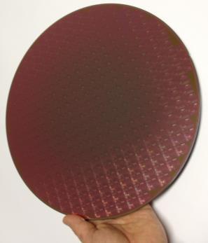
8 Fabrication : 200 nm versus 300 nm 200mm wafer 300mm wafer High volume Sub-65nm CMOS node 193nm immersion photolithography Sub-50nm resolution Zoom ~750 Million! Wafer thickness uniformity < ±5nm on 300-mm ~ ±10nm on 200-mm >55 Million ring resonators! Fabrication Crolles 2 (Fr)

9 Silicon optical modulator: phase shifter Carrier depletion in interleaved pn diode
10 DC transmission characterisation Interleaved pn diode Phase shifter efficiency (V p L p ) Active region 0V MMI loss Waveguide loss V.cm ~ 2.1 db/mm 0.7 to 0.9 db < 1 db/cm
11 RF characteristics Mach Zehnder interferometer : 950 µm active region -3dB cut-off frequency > 20 GHz
 Total on chip loss @ operating point of high extinction ratio Interleaved pn diode 7.")
12 40 Gbit/s data transmission Mach Zehnder interferometer : 950 µm active region 40 Gbit/s Extinction ratio (L=0.95 mm) Total on chip operating point of high extinction ratio Interleaved pn diode 7.8 db 4 db

13 Silicon optical modulator ITRS: Optical interconnect ( ) A large variety of CMOS compatible modulators have been proposed in the literature ( ) ( ) significant progress has been made ( ) The primary challenges for optical interconnects at the present time are producing cost effective, low power components. Short distance and high volume applications (electrical bottleneck) Optical cables Data-center Main challenges: Driving voltage of modulator Power consumption Electroabsorption modulator
14 Power consumption ~3 pj/bit ~0.5 to 1 pj/bit?
15 Outline Introduction Carrier depletion based silicon optical modulators fabricated on 300 mm SOI wafers Ge/SiGe quantum well electroabsorption modulator Conclusion
16 Electroabsorption in group IV materials Bandgap Bulk-Si Bulk-Ge Direct Indirect 3.3 ev 0.37µm 1.13 ev 1.1µm 0.8 ev 1.55 µm 0.66 ev 1.88µm Silicon : transparent at l > 1.1 µm, and indirect bandgap material => Electroabsorption is not possible at telecommunication wavelengths Germanium : indirect gap material with direct gap properties, at telecommunication wavelengths.
17 Electroabsorption in QW structures Quantum confined Stark effect (QCSE) a E=0 E 0 l Excitonic peak reduction and red-shift absorption spectra with electrical field
18 Active region design and growth Si 0.15 Ge nm SiGe n-type SiGe spacer QWs SiGe spacer Ge 10 nm Si 0.15 Ge nm SiGe p-type Si 0.1 Ge 0.9 relaxed buffer QW structure: 10 nm Ge well/ 15 nm Si 0.15 Ge 0.85 barrier Strain-compensated structure Average Ge in MQWs = 90% => Si 0.1 Ge 0.9 buffer Graded buffer from Si to Si 0.1 Ge 0.9 Si(100) 4.2% lattice mismatch between Si and Ge
19 Active region design and growth Si 0.15 Ge nm Si 0.1 Ge 0.9 n-type Si 0.1 Ge 0.9 spacer QWs Si 0.1 Ge 0.9 spacer Ge 10 nm Si 0.15 Ge nm Si 0.1 Ge 0.9 p-type Si 0.1 Ge 0.9 relaxed buffer Graded buffer from Si to Si 0.1 Ge 0.9 Low-rate growth (~0.3 nm/s) for optimum layer and interface control Around 1 hr Ge QW Low Energy Plasma Enhanced Chemical Vapour Deposition High-rate growth (5-10 nm/s) (LEPECVD) 40 minutes for 13 µm buffer Si(100) LEPECVD Graded buffer : TDD (Threading dislocation denstity) ~ 10 6 cm -2 G. Isella, D. Chrastina, J. Frigerio


20 Electroabsorption modulator Ge/SiGe quantum well modulator 20 periods of Ge/SiGe QW 90 µm 3 µm 1 µm Light
21 Static performance: optical transmission Ge/SiGe quantum well modulator ~6x10 4 V/cm ~7.5x10 4 V/cm Bias from 0 to 5V : Extinction Ratio (ER) > 6 db for 20 nm range Insertion Loss (IL) : 5 to 15 db Overlap with virtual substrate ~3x10 4 V/cm ~4.5x10 4 V/cm
22 Static performance: optical transmission Ge/SiGe quantum well modulator ~6x10 4 V/cm ~7.5x10 4 V/cm Bias from 0 to 5V : Extinction Ratio (ER) > 6 db for 20 nm range Insertion Loss (IL) : 5 to 15 db Overlap with virtual substrate ~3x10 4 V/cm ~4.5x10 4 V/cm Bias from 3 to 4V (1V swing) ER > 6 db for 5nm range
23 High frequency performance Ge/SiGe QW modulator -3dB cut-off frequency > 20 GHz

24 Power consumption ~3 pj/bit ~0.5 to 1 pj/bit 70 fj/bit


25 Ge/SiGe QW modulator : on-going work Design of a Ge/SiGe modulator on SOI 1.3 µm Wavelength ~ 1440 nm Towards operation at 1.3µm: Increase of compressive strain in Ge wells 10 nm Ge well/ 15 nm Si 0.15 Ge 0.85 barrier strained-balanced on Si 0.1 Ge 0.9 buffer 10 nm Ge well/ 15 nm Si 0.35 Ge 0.65 barrier strained-balanced on Si 0.21 Ge 0.79 buffer Ge well: Compressive strain Si 0.15 Ge 0.85 barrier: Tensile strain
26 Ge/SiGe QW : 1.3 µm Surface illuminated diode : photocurrent measurement
27 Ge/SiGe QW modulator : integration on SOI Si 0.1 Ge 0.9 n-type Si 0.1 Ge 0.9 spacer QWs Si 0.1 Ge 0.9 spacer Si 0.15 Ge nm Ge 10 nm Si 0.15 Ge nm Si 0.1 Ge 0.9 p-type Si 0.1 Ge 0.9 relaxed buffer Graded buffer from Si to Si 0.1 Ge 0.9 Graded buffer from Si to Si 0.1 Ge 0.9 Si(100) Si(100) Schematic description Real scale Challenge : light coupling from silicon to QW region?
28 Ge/SiGe QW modulator : integration on SOI Challenge : reduction of the buffer thickness keeping high quality structures and good material properties Thin buffer Si(100) Graded buffer from Si to Si 0.1 Ge 0.9 Si(100) New process development : 360 nm thick Si 0.08 Ge 0.92 buffer obtained by the sequentially growing of four 90 nm thick Si 0.08 Ge 0.92 films. Each growth performed at 400 followed by thermal annealing at 780 to reduce dislocation density and to form a relaxed buffer layer G. Isella
29 Growth and characterization Ge/SiGe QW : QCSE on thin buffer Surface illuminated diode : photocurrent measurement Low dislocation density Good QCSE is observed.

30 Design of the modulator Ge/SiGe QW modulator : design of the integrated modualtor Estimated performance : 4 db loss and 7.7 db extinction ratio On going work : fabrication
31 Conclusion : silicon based optical modulator Carrier depletion based silicon modulators : Fabrication in 300 mm SOI wafers Good performances : Mach Zehnder modulator : extinction ratio : 7.9 db ER and insertion loss = 4 db Ge/SiGe QW modulators : The solution to achieve energy consumption < 100 fj / bit First demonstration : extinction ration > 6 db, cut off frequency > 20 GHz Challenge : integration on SOI Preliminary results : development of thin buffer, active region design to work at 1.3 µm


32 Acknowledgments P. Chaisakul G. Rasigade M. Ziebel M-S. Rouifed D. Perez-Galacho D. Bouville S. Edmond X. Le Roux P. Crozat L. Vivien Funding S. Menezo J-M. Fédéli N. Vulliet P. Rivallin S. Olivier J-M. Hartman L. Virot A. Souhaité C. Baudot F. Boeuf G. Isella D. Chrastina J. Frigerio
New advances in silicon photonics Delphine Marris-Morini
 New advances in silicon photonics Delphine Marris-Morini P. Brindel Alcatel-Lucent Bell Lab, Nozay, France New Advances in silicon photonics D. Marris-Morini, L. Virot*, D. Perez-Galacho, X. Le Roux, D.
Silicon photonics: Optical modulation in silicon platform
 Silicon Photonics Silicon-based micro and nanophotonic devices Silicon photonics: Optical modulation in silicon platform, Institut d Electronique Fondamentale, CNRS UMR 8622, Université Paris Sud, 91405
Lecture: Integration of silicon photonics with electronics. Prepared by Jean-Marc FEDELI CEA-LETI
 Lecture: Integration of silicon photonics with electronics Prepared by Jean-Marc FEDELI CEA-LETI Context The goal is to give optical functionalities to electronics integrated circuit (EIC) The objectives
Simplified model enabling optimization of silicon modulators
 Simplified model enabling optimization of silicon modulators Diego Perez-Galacho, Delphine Marris-Morini, Remco Stoffer, Eric Cassan, Charles Baudot, Twan Korthorst, Frederic Boeuf, Laurent Vivien To cite
Polarization insensitive Ge-rich silicon germanium waveguides for optical interconnects on silicon
 Polarization insensitive Ge-rich silicon germanium waveguides for optical interconnects on silicon V Vakarin, Papichaya Chaisakul, Jacopo Frigerio, Andrea Ballabio, Joan Manel Ramírez, Xavier Le Roux,
Silicon Optical Modulator
 Silicon Optical Modulator Silicon Optical Photonics Nature Photonics Published online: 30 July 2010 Byung-Min Yu 24 April 2014 High-Speed Circuits & Systems Lab. Dept. of Electrical and Electronic Engineering
Silicon Photonics Photo-Detector Announcement. Mario Paniccia Intel Fellow Director, Photonics Technology Lab
 Silicon Photonics Photo-Detector Announcement Mario Paniccia Intel Fellow Director, Photonics Technology Lab Agenda Intel s Silicon Photonics Research 40G Modulator Recap 40G Photodetector Announcement
Silicon Carrier-Depletion-Based Mach-Zehnder and Ring Modulators with Different Doping Patterns for Telecommunication and Optical Interconnect
 Silicon Carrier-Depletion-Based Mach-Zehnder and Ring Modulators with Different Doping Patterns for Telecommunication and Optical Interconnect Hui Yu, Marianna Pantouvaki*, Joris Van Campenhout*, Katarzyna
Silicon Photonics Technology Platform To Advance The Development Of Optical Interconnects
 Silicon Photonics Technology Platform To Advance The Development Of Optical Interconnects By Mieke Van Bavel, science editor, imec, Belgium; Joris Van Campenhout, imec, Belgium; Wim Bogaerts, imec s associated
ECEN689: Special Topics in Optical Interconnects Circuits and Systems Spring 2016
 ECEN689: Special Topics in Optical Interconnects Circuits and Systems Spring 2016 Lecture 10: Electroabsorption Modulator Transmitters Sam Palermo Analog & Mixed-Signal Center Texas A&M University Announcements
A 3.9 ns 8.9 mw 4 4 Silicon Photonic Switch Hybrid-Integrated with CMOS Driver
 A 3.9 ns 8.9 mw 4 4 Silicon Photonic Switch Hybrid-Integrated with CMOS Driver A. Rylyakov, C. Schow, B. Lee, W. Green, J. Van Campenhout, M. Yang, F. Doany, S. Assefa, C. Jahnes, J. Kash, Y. Vlasov IBM
HIGH-EFFICIENCY MQW ELECTROABSORPTION MODULATORS
 HIGH-EFFICIENCY MQW ELECTROABSORPTION MODULATORS J. Piprek, Y.-J. Chiu, S.-Z. Zhang (1), J. E. Bowers, C. Prott (2), and H. Hillmer (2) University of California, ECE Department, Santa Barbara, CA 93106
MICRO RING MODULATOR. Dae-hyun Kwon. High-speed circuits and Systems Laboratory
 MICRO RING MODULATOR Dae-hyun Kwon High-speed circuits and Systems Laboratory Paper preview Title of the paper Low Vpp, ultralow-energy, compact, high-speed silicon electro-optic modulator Publication
A low-power, high-speed, 9-channel germaniumsilicon electro-absorption modulator array integrated with digital CMOS driver and wavelength multiplexer
 A low-power, high-speed, 9-channel germaniumsilicon electro-absorption modulator array integrated with digital CMOS driver and wavelength multiplexer A. V. Krishnamoorthy, 1* X. Zheng, 1 D. Feng, 3 J.
Intersubband spectroscopy of electron tunneling in GaN/AlN coupled quantum wells
 Intersubband spectroscopy of electron tunneling in GaN/AlN coupled quantum wells N. Kheirodin, L. Nevou, M. Tchernycheva, F. H. Julien, A. Lupu, P. Crozat, L. Meignien, E. Warde, L.Vivien Institut d Electronique
Optical modulation by carrier depletion in a silicon PIN diode
 Optical modulation by carrier depletion in a silicon PIN diode Delphine Marris-Morini, Xavier Le Roux, Laurent Vivien, Eric Cassan, Daniel Pascal, Mathieu Halbwax, Sylvain Maine, Suzanne Laval Institut
Silicon Photonics: an Industrial Perspective
 Silicon Photonics: an Industrial Perspective Antonio Fincato Advanced Programs R&D, Cornaredo, Italy OUTLINE 2 Introduction Silicon Photonics Concept 300mm (12 ) Photonic Process Main Silicon Photonics
Lecture 9 External Modulators and Detectors
 Optical Fibres and Telecommunications Lecture 9 External Modulators and Detectors Introduction Where are we? A look at some real laser diodes. External modulators Mach-Zender Electro-absorption modulators
The Past, Present, and Future of Silicon Photonics
 The Past, Present, and Future of Silicon Photonics Myung-Jae Lee High-Speed Circuits & Systems Lab. Dept. of Electrical and Electronic Engineering Yonsei University Outline Introduction A glance at history
Si CMOS Technical Working Group
 Si CMOS Technical Working Group CTR, Spring 2008 meeting Markets Interconnects TWG Breakouts Reception TWG reports Si CMOS: photonic integration E-P synergy - Integration - Standardization - Cross-market
NEXT GENERATION SILICON PHOTONICS FOR COMPUTING AND COMMUNICATION PHILIPPE ABSIL
 NEXT GENERATION SILICON PHOTONICS FOR COMPUTING AND COMMUNICATION PHILIPPE ABSIL OUTLINE Introduction Platform Overview Device Library Overview What s Next? Conclusion OUTLINE Introduction Platform Overview
Electronic-Photonic ICs for Low Cost and Scalable Datacenter Solutions
 Electronic-Photonic ICs for Low Cost and Scalable Datacenter Solutions Christoph Theiss, Director Packaging Christoph.Theiss@sicoya.com 1 SEMICON Europe 2016, October 27 2016 Sicoya Overview Spin-off from
Silicon Photonics in Optical Communications. Lars Zimmermann, IHP, Frankfurt (Oder), Germany
, Germany") Silicon Photonics in Optical Communications Lars Zimmermann, IHP, Frankfurt (Oder), Germany Outline IHP who we are Silicon photonics Photonic-electronic integration IHP photonic technology Conclusions
Silicon Photonics in Optical Communications Lars Zimmermann, IHP, Frankfurt (Oder), Germany Outline IHP who we are Silicon photonics Photonic-electronic integration IHP photonic technology Conclusions
Semiconductor Optical Communication Components and Devices Lecture 39: Optical Modulators
 Semiconductor Optical Communication Components and Devices Lecture 39: Optical Modulators Prof. Utpal Das Professor, Department of Electrical Engineering, Laser Technology Program, Indian Institute of
Roadmap on silicon photonics
 Home Search Collections Journals About Contact us My IOPscience Roadmap on silicon photonics This content has been downloaded from IOPscience. Please scroll down to see the full text. View the table of
Silicon Photonics Opportunity, applications & Recent Results
 Silicon Photonics Opportunity, applications & Recent Results Dr. Mario Paniccia Intel Fellow Director, Photonics Technology Lab Intel Corporation www.intel.com/go/sp Purdue University Oct 5 2007 Agenda
The Light at the End of the Wire. Dana Vantrease + HP Labs + Mikko Lipasti
 The Light at the End of the Wire Dana Vantrease + HP Labs + Mikko Lipasti 1 Goals of This Talk Why should we (architects) be interested in optics? How does on-chip optics work? What can we build with optics?
Silicon high-speed binary phase-shift keying modulator with a single-drive push pull high-speed traveling wave electrode
 58 Photon. Res. / Vol. 3, No. 3 / June 2015 Wang et al. Silicon high-speed binary phase-shift keying modulator with a single-drive push pull high-speed traveling wave electrode Jinting Wang, 1 Linjie Zhou,
Optical Interconnection in Silicon LSI
 The Fifth Workshop on Nanoelectronics for Tera-bit Information Processing, 1 st Century COE, Hiroshima University Optical Interconnection in Silicon LSI Shin Yokoyama, Yuichiro Tanushi, and Masato Suzuki
Performance of silicon micro ring modulator with an interleaved p-n junction for optical interconnects
 Indian Journal of Pure & Applied Physics Vol. 55, May 2017, pp. 363-367 Performance of silicon micro ring modulator with an interleaved p-n junction for optical interconnects Priyanka Goyal* & Gurjit Kaur
Index. Cambridge University Press Silicon Photonics Design Lukas Chrostowski and Michael Hochberg. Index.
 absorption, 69 active tuning, 234 alignment, 394 396 apodization, 164 applications, 7 automated optical probe station, 389 397 avalanche detector, 268 back reflection, 164 band structures, 30 bandwidth
OPTICAL I/O RESEARCH PROGRAM AT IMEC
 OPTICAL I/O RESEARCH PROGRAM AT IMEC IMEC CORE CMOS PHILIPPE ABSIL, PROGRAM DIRECTOR JORIS VAN CAMPENHOUT, PROGRAM MANAGER SCALING TRENDS IN CHIP-LEVEL I/O RECENT EXAMPLES OF HIGH-BANDWIDTH I/O Graphics
Silicon-On-Insulator based guided wave optical clock distribution
 Silicon-On-Insulator based guided wave optical clock distribution K. E. Moselund, P. Dainesi, and A. M. Ionescu Electronics Laboratory Swiss Federal Institute of Technology People and funding EPFL Project
Physics of Waveguide Photodetectors with Integrated Amplification
 Physics of Waveguide Photodetectors with Integrated Amplification J. Piprek, D. Lasaosa, D. Pasquariello, and J. E. Bowers Electrical and Computer Engineering Department University of California, Santa
Near/Mid-Infrared Heterogeneous Si Photonics
 PHOTONICS RESEARCH GROUP Near/Mid-Infrared Heterogeneous Si Photonics Zhechao Wang, PhD Photonics Research Group Ghent University / imec, Belgium ICSI-9, Montreal PHOTONICS RESEARCH GROUP 1 Outline Ge-on-Si
High-speed modulation of a compact silicon ring resonator based on a reverse-biased pn diode
 High-speed modulation of a compact silicon ring resonator based on a reverse-biased pn diode F.Y. Gardes 1 *, A. Brimont 2, P. Sanchis 2, G. Rasigade 3, D. Marris-Morini 3, L. O'Faolain 4, F. Dong 4, J.M.
ECEN689: Special Topics in Optical Interconnects Circuits and Systems Spring 2016
 ECEN689: Special Topics in Optical Interconnects Circuits and Systems Spring 2016 Lecture 9: Mach-Zehnder Modulator Transmitters Sam Palermo Analog & Mixed-Signal Center Texas A&M University Mach-Zehnder
InP-based Waveguide Photodetector with Integrated Photon Multiplication
 InP-based Waveguide Photodetector with Integrated Photon Multiplication D.Pasquariello,J.Piprek,D.Lasaosa,andJ.E.Bowers Electrical and Computer Engineering Department University of California, Santa Barbara,
Heinrich-Hertz-Institut Berlin
 NOVEMBER 24-26, ECOLE POLYTECHNIQUE, PALAISEAU OPTICAL COUPLING OF SOI WAVEGUIDES AND III-V PHOTODETECTORS Ludwig Moerl Heinrich-Hertz-Institut Berlin Photonic Components Dept. Institute for Telecommunications,,
Ultra-low voltage resonant tunnelling diode electroabsorption modulator
 Ultra-low voltage resonant tunnelling diode electroabsorption modulator, 1/10 Ultra-low voltage resonant tunnelling diode electroabsorption modulator J. M. L. FIGUEIREDO Faculdade de Ciências e Tecnologia,
A Fully Integrated 20 Gb/s Optoelectronic Transceiver Implemented in a Standard
 A Fully Integrated 20 Gb/s Optoelectronic Transceiver Implemented in a Standard 0.13 µm CMOS SOI Technology School of Electrical and Electronic Engineering Yonsei University 이슬아 1. Introduction 2. Architecture
Optical Integrated Devices in Silicon On Insulator for VLSI Photonics
 Optical Integrated Devices in Silicon On Insulator for VLSI Photonics Design, Modelling, Fabrication & Characterization Piero Orlandi 1 Possible Approaches Reduced Design time Transparent Technology Shared
Lecture 4 INTEGRATED PHOTONICS
 Lecture 4 INTEGRATED PHOTONICS What is photonics? Photonic applications use the photon in the same way that electronic applications use the electron. Devices that run on light have a number of advantages
SiGe BiCMOS and Photonic technologies for high frequency and communication applications Andreas Mai
 SiGe BiCMOS and Photonic technologies for high frequency and communication applications Andreas Mai Department Head Technology Outline Introduction & Motivation SiGe HBT device developments for high RF
A CMOS-compatible silicon photonic platform for high-speed integrated opto-electronics
 Invited Paper A CMOS-compatible silicon photonic platform for high-speed integrated opto-electronics Christophe Galland 1, Ari Novack 3,4, Yang Liu 1, Ran Ding 1, Michael Gould 2, Tom Baehr-Jones 1, Qi
Module 16 : Integrated Optics I
 Module 16 : Integrated Optics I Lecture : Integrated Optics I Objectives In this lecture you will learn the following Introduction Electro-Optic Effect Optical Phase Modulator Optical Amplitude Modulator
Convergence Challenges of Photonics with Electronics
 Convergence Challenges of Photonics with Electronics Edward Palen, Ph.D., P.E. PalenSolutions - Optoelectronic Packaging Consulting www.palensolutions.com palensolutions@earthlink.net 415-850-8166 October
High-speed Ge photodetector monolithically integrated with large cross silicon-on-insulator waveguide
 [ APPLIED PHYSICS LETTERS ] High-speed Ge photodetector monolithically integrated with large cross silicon-on-insulator waveguide Dazeng Feng, Shirong Liao, Roshanak Shafiiha. etc Contents 1. Introduction
Modulation of light. Direct modulation of sources Electro-absorption (EA) modulators
 modulators") Modulation of light Direct modulation of sources Electro-absorption (EA) modulators Why Modulation A communication link is established by transmission of information reliably Optical modulation is embedding
Modulation of light Direct modulation of sources Electro-absorption (EA) modulators Why Modulation A communication link is established by transmission of information reliably Optical modulation is embedding
Graphene electro-optic modulator with 30 GHz bandwidth
 Graphene electro-optic modulator with 30 GHz bandwidth Christopher T. Phare 1, Yoon-Ho Daniel Lee 1, Jaime Cardenas 1, and Michal Lipson 1,2,* 1School of Electrical and Computer Engineering, Cornell University,
Optical Interconnect to Chips
 Optical Interconnect to Chips David A. B. Miller Stanford University http://ee.stanford.edu/~dabm 2/29/08 Computing of the Future, David A. B. Miller, Stanford 1 Summary Wiring, optics, and communicating
A silicon avalanche photodetector fabricated with standard CMOS technology with over 1 THz gain-bandwidth product
 A silicon avalanche photodetector fabricated with standard CMOS technology with over 1 THz gain-bandwidth product Myung-Jae Lee and Woo-Young Choi* Department of Electrical and Electronic Engineering,
for optical communication system
 High speed Ge waveguide detector for optical communication system Xingjun Wang, Zhijuan Tu and Zhiping Zhou State Key Laboratory of Advanced Optical Communication Systems and Networks, School of Electronics
Optical IQ modulators for coherent 100G and beyond
 for coherent 1G and beyond By GARY WANG Indium phosphide can overcome the limitations of LiNbO3, opening the door to the performance tomorrow s coherent transmission systems will require. T HE CONTINUED
Lecture 18: Photodetectors
 Lecture 18: Photodetectors Contents 1 Introduction 1 2 Photodetector principle 2 3 Photoconductor 4 4 Photodiodes 6 4.1 Heterojunction photodiode.................... 8 4.2 Metal-semiconductor photodiode................
50-Gb/s silicon optical modulator with travelingwave
 5-Gb/s silicon optical modulator with travelingwave electrodes Xiaoguang Tu, 1, * Tsung-Yang Liow, 1 Junfeng Song, 1,2 Xianshu Luo, 1 Qing Fang, 1 Mingbin Yu, 1 and Guo-Qiang Lo 1 1 Institute of Microelectronics,
Fabrication of High-Speed Resonant Cavity Enhanced Schottky Photodiodes
 Fabrication of High-Speed Resonant Cavity Enhanced Schottky Photodiodes Abstract We report the fabrication and testing of a GaAs-based high-speed resonant cavity enhanced (RCE) Schottky photodiode. The
InP-based Waveguide Photodetector with Integrated Photon Multiplication
 InP-based Waveguide Photodetector with Integrated Photon Multiplication D.Pasquariello,J.Piprek,D.Lasaosa,andJ.E.Bowers Electrical and Computer Engineering Department University of California, Santa Barbara,
Ultralinear heterogeneously integrated ring-assisted Mach Zehnder interferometer modulator on silicon
 Research Article Vol. 3, No. 12 / December 2016 / Optica 1483 Ultralinear heterogeneously integrated ring-assisted Mach Zehnder interferometer modulator on silicon CHONG ZHANG, 1, *PAUL A. MORTON, 2 JACOB
Analog Characterization of Low-Voltage MQW Traveling-Wave Electroabsorption Modulators
 JOURNAL OF LIGHTWAVE TECHNOLOGY, VOL. 21, NO. 12, DECEMBER 2003 3011 Analog Characterization of Low-Voltage MQW Traveling-Wave Electroabsorption Modulators Bin Liu, Member, IEEE, Jongin Shim, Member, IEEE,
Silicon Photonics: A Platform for Integration, Wafer Level Assembly and Packaging
 Silicon Photonics: A Platform for Integration, Wafer Level Assembly and Packaging M. Asghari Kotura Inc April 27 Contents: Who is Kotura Choice of waveguide technology Challenges and merits of Si photonics
Semiconductor Optical Active Devices for Photonic Networks
 UDC 621.375.8:621.38:621.391.6 Semiconductor Optical Active Devices for Photonic Networks VKiyohide Wakao VHaruhisa Soda VYuji Kotaki (Manuscript received January 28, 1999) This paper describes recent
High Speed pin Photodetector with Ultra-Wide Spectral Responses
 High Speed pin Photodetector with Ultra-Wide Spectral Responses C. Tam, C-J Chiang, M. Cao, M. Chen, M. Wong, A. Vazquez, J. Poon, K. Aihara, A. Chen, J. Frei, C. D. Johns, Ibrahim Kimukin, Achyut K. Dutta
CMOS-compatible dual-output silicon modulator for analog signal processing
 CMOS-compatible dual-output silicon modulator for analog signal processing S. J. Spector 1*, M. W. Geis 1, G.-R.Zhou 2, M. E. Grein 1, F. Gan 2, M.A. Popović 2, J. U. Yoon 1, D. M. Lennon 1, E. P. Ippen
Optical Bus for Intra and Inter-chip Optical Interconnects
 Optical Bus for Intra and Inter-chip Optical Interconnects Xiaolong Wang Omega Optics Inc., Austin, TX Ray T. Chen University of Texas at Austin, Austin, TX Outline Perspective of Optical Backplane Bus
IEEE JOURNAL OF SELECTED TOPICS IN QUANTUM ELECTRONICS 2010 Silicon Photonic Circuits: On-CMOS Integration, Fiber Optical Coupling, and Packaging
 IEEE JOURNAL OF SELECTED TOPICS IN QUANTUM ELECTRONICS 2010 Silicon Photonic Circuits: On-CMOS Integration, Fiber Optical Coupling, and Packaging Christophe Kopp, St ephane Bernab e, Badhise Ben Bakir,
Integration of Optoelectronic and RF Devices for Applications in Optical Interconnect and Wireless Communication
 Integration of Optoelectronic and RF Devices for Applications in Optical Interconnect and Wireless Communication Zhaoran (Rena) Huang Assistant Professor Department of Electrical, Computer and System Engineering
Alternatives to standard MOSFETs. What problems are we really trying to solve?
 Alternatives to standard MOSFETs A number of alternative FET schemes have been proposed, with an eye toward scaling up to the 10 nm node. Modifications to the standard MOSFET include: Silicon-in-insulator
Nanophotonics for low latency optical integrated circuits
 Nanophotonics for low latency optical integrated circuits Akihiko Shinya NTT Basic Research Labs., Nanophotonics Center, NTT Corporation MPSoC 17, Annecy, France Outline Low latency optical circuit BDD
A 25 Gb/s Silicon Photonics Platform
 A 25 Gb/s Silicon Photonics Platform Tom Baehr-Jones 1,*, Ran Ding 1, Ali Ayazi 1, Thierry Pinguet 1, Matt Streshinsky 1, Nick Harris 1, Jing Li 1, Li He 1, Mike Gould 1, Yi Zhang 1, Andy Eu-Jin Lim 2,
Offline Optimization of Wavelength Allocation and Laser to Deal with Energy-Performance Tradeoffs in Nanophotonic Interconnects
 Offline Optimization of Wavelength Allocation and Laser to Deal with Energy-Performance Tradeoffs in Nanophotonic Interconnects Cédric KILLIAN Universty of Rennes 1 Cairn Team IRISA, Inria OPTICS workshop,
Resonant Tunneling Device. Kalpesh Raval
 Resonant Tunneling Device Kalpesh Raval Outline Diode basics History of Tunnel diode RTD Characteristics & Operation Tunneling Requirements Various Heterostructures Fabrication Technique Challenges Application
Si and InP Integration in the HELIOS project
 Si and InP Integration in the HELIOS project J.M. Fedeli CEA-LETI, Grenoble ( France) ECOC 2009 1 Basic information about HELIOS HELIOS photonics ELectronics functional Integration on CMOS www.helios-project.eu
Comparison between strip and rib SOI microwaveguides for intra-chip light distribution
 Optical Materials 27 (2005) 756 762 www.elsevier.com/locate/optmat Comparison between strip and rib SOI microwaveguides for intra-chip light distribution L. Vivien a, *, F. Grillot a, E. Cassan a, D. Pascal
Ge/SiGe asymmetric Fabry-Perot quantum well electroabsorption modulators
 Ge/SiGe asymmetric Fabry-Perot quantum well electroabsorption modulators Elizabeth H. Edwards,1, Ross M. Audet, 1 Edward T. Fei, 1 Stephanie A. Claussen, 1 Rebecca K. Schaevitz, 2 Emel Tasyurek, 1 Yiwen
What is the highest efficiency Solar Cell?
 What is the highest efficiency Solar Cell? GT CRC Roof-Mounted PV System Largest single PV structure at the time of it s construction for the 1996 Olympic games Produced more than 1 billion watt hrs. of
Silicon-Organic hybrid Fabrication platform for Integrated circuits FP7-ICT GA No
 www.sofi-ict.eu FP7-ICT-2009.3.8 GA No. 248609 Participants: 2 Outline Today s High Speed Interconnects Vision : Convergence of Photonics & Electronics Silicon Photonics Technology Silicon-Organic Hybrid
SILICON PHOTONICS FOR DATA COMMUNICATIONS
 SILICON PHOTONICS FOR DATA COMMUNICATIONS Gideon Yoffe Kaiam Corporation, California Visitor at ICT, KTH Kista Introduction Kaiam packaging technology Data communication, Datacenters Silicon Photonics
EE 232 Lightwave Devices Optical Interconnects
 EE 232 Lightwave Devices Optical Interconnects Sajjad Moazeni Department of Electrical Engineering & Computer Sciences University of California, Berkeley 1 Emergence of Optical Links US IT Map Hyper-Scale
Photonic Integrated Circuits Made in Berlin
 Fraunhofer Heinrich Hertz Institute Photonic Integrated Circuits Made in Berlin Photonic integration Workshop, Columbia University, NYC October 2015 Moritz Baier, Francisco M. Soares, Norbert Grote Fraunhofer
Silicon Photonics: A Review
 IOSR Journal of Applied Physics (IOSR-JAP) e-issn: 2278-4861. Volume 3, Issue 5 (Mar. - Apr. 2013), PP 67-79 Silicon Photonics: A Review Ashish Dhiman 1 ( Department of Electronics and Communication, Delhi
A tunable Si CMOS photonic multiplexer/de-multiplexer
 A tunable Si CMOS photonic multiplexer/de-multiplexer OPTICS EXPRESS Published : 25 Feb 2010 MinJae Jung M.I.C.S Content 1. Introduction 2. CMOS photonic 1x4 Si ring multiplexer Principle of add/drop filter
Examination Optoelectronic Communication Technology. April 11, Name: Student ID number: OCT1 1: OCT 2: OCT 3: OCT 4: Total: Grade:
 Examination Optoelectronic Communication Technology April, 26 Name: Student ID number: OCT : OCT 2: OCT 3: OCT 4: Total: Grade: Declaration of Consent I hereby agree to have my exam results published on
Robert G. Hunsperger. Integrated Optics. Theory and Technology. Sixth Edition. 4ü Spri rineer g<
 Robert G. Hunsperger Integrated Optics Theory and Technology Sixth Edition 4ü Spri rineer g< 1 Introduction 1 1.1 Advantages of Integrated Optics 2 1.1.1 Comparison of Optical Fibers with Other Interconnectors
Optoelectronic integrated circuits incorporating negative differential resistance devices
 Optoelectronic integrated circuits incorporating negative differential resistance devices José Figueiredo Centro de Electrónica, Optoelectrónica e Telecomunicações Departamento de Física da Faculdade de
Compact Low-power-consumption Optical Modulator
 Compact Low-power-consumption Modulator Eiichi Yamada, Ken Tsuzuki, Nobuhiro Kikuchi, and Hiroshi Yasaka Abstract modulators are indispensable devices for optical fiber communications. They turn light
Research Article Room Temperature Direct Band Gap Emission from Ge p-i-n Heterojunction Photodiodes
 OptoElectronics Volume 22, Article ID 96275, 4 pages doi:.55/22/96275 Research Article Room Temperature Direct Band Gap Emission from Ge p-i-n Heterojunction Photodiodes E. Kasper, M. Oehme, T. Arguirov,
Heterogeneously Integrated Microwave Signal Generators with Narrow- Linewidth Lasers
 Heterogeneously Integrated Microwave Signal Generators with Narrow- Linewidth Lasers John E. Bowers, Jared Hulme, Tin Komljenovic, Mike Davenport and Chong Zhang Department of Electrical and Computer Engineering
Heterogeneous Integration of Silicon and AlGaInAs for a Silicon Evanescent Laser
 Invited Paper Heterogeneous Integration of Silicon and AlGaInAs for a Silicon Evanescent Laser Alexander W. Fang a, Hyundai Park a, Richard Jones b, Oded Cohen c, Mario J. Paniccia b, and John E. Bowers
Improved RF Power Extraction from 1.55 m Ge-on-SOI PIN Photodiodes with Load Impedance Optimization
 Improved RF Power Extraction from 1.55 m Ge-on-SOI PIN Photodiodes with Load Impedance Optimization A Thesis Presented to the Electrical Engineering Department Faculty of California Polytechnic State University,
EPIC: The Convergence of Electronics & Photonics
 EPIC: The Convergence of Electronics & Photonics K-Y Tu, Y.K. Chen, D.M. Gill, M. Rasras, S.S. Patel, A.E. White ell Laboratories, Lucent Technologies M. Grove, D.C. Carothers, A.T. Pomerene, T. Conway
40 Gb/s silicon photonics modulator for TE and TM polarisations
 40 Gb/s silicon photonics modulator for TE and TM polarisations F. Y. Gardes,* D. J. Thomson, N. G. Emerson and G. T. Reed Advanced Technology Institute, University of Surrey Guildford, Surrey, GU2 7XH,
Integrated electro-optical waveguide based devices with liquid crystals on a silicon backplane
 Integrated electro-optical waveguide based devices with liquid crystals on a silicon backplane Florenta Costache Group manager Smart Micro-Optics SMO/AMS Fraunhofer Institute for Photonic Microsystems,
Hybrid silicon modulators
 280 CHINESE OPTICS LETTERS / Vol. 7, No. 4 / April 10, 2009 Hybrid silicon modulators Invited Paper Hui-Wen Chen, Yinghao Kuo, and J. E. Bowers Department of Electrical and Computer Engineering, University
Architecture of Silicon Photonic Links
 UNIVERSITE PARIS-SUD ÉCOLE DOCTORALE Sciences et Technologie de l Information, des Télécommunications et des Systèmes Laboratoire de Institut d'electronique Fondamentale DISCIPLINE : Physique THÈSE DE
Contents Silicon Photonic Wire Waveguides: Fundamentals and Applications
 1 Silicon Photonic Wire Waveguides: Fundamentals and Applications.. 1 Koji Yamada 1.1 Introduction... 1 1.2 Fundamental Design of Silicon Photonic Wire Waveguides... 3 1.2.1 Guided Modes... 3 1.2.2 Effect
ATV 2011: Computer Engineering
 ATV 2011: Technology Trends in Computer Engineering Professor Per Larsson-Edefors ATV 2011, L1, Per Larsson-Edefors Page 1 Solid-State Devices www.cse.chalmers.se/~perla/ugrad/ SemTech/Lectures_2000.pdf
Design and fabrication of indium phosphide air-bridge waveguides with MEMS functionality
 Design and fabrication of indium phosphide air-bridge waveguides with MEMS functionality Wing H. Ng* a, Nina Podoliak b, Peter Horak b, Jiang Wu a, Huiyun Liu a, William J. Stewart b, and Anthony J. Kenyon
Optical MEMS in Compound Semiconductors Advanced Engineering Materials, Cal Poly, SLO November 16, 2007
 Optical MEMS in Compound Semiconductors Advanced Engineering Materials, Cal Poly, SLO November 16, 2007 Outline Brief Motivation Optical Processes in Semiconductors Reflectors and Optical Cavities Diode
High-Speed Scalable Silicon-MoS 2 P-N Heterojunction Photodetectors
 High-Speed Scalable Silicon-MoS 2 P-N Heterojunction Photodetectors Veerendra Dhyani 1, and Samaresh Das 1* 1 Centre for Applied Research in Electronics, Indian Institute of Technology Delhi, New Delhi-110016,