ATV 2011: Computer Engineering
|
|
|
- Percival Glenn
- 6 years ago
- Views:
Transcription
1 ATV 2011: Technology Trends in Computer Engineering Professor Per Larsson-Edefors ATV 2011, L1, Per Larsson-Edefors Page 1 Solid-State Devices SemTech/Lectures_2000.pdf ATV 2011, L1, Per Larsson-Edefors Page 2 1
. Si at T = 300 K: 10 10 free carriers/cm 3.")
2 Semiconductors E g for Si is 1.12 ev E g for SiO 2 is 8.9 ev! 1 ev = J ATV 2011, L1, Per Larsson-Edefors Page 3 Carriers and Temperature Semiconductor with no impurities is intrinsic. Electrons in valence band may be excited to conduction band, jumping the band gap (#electrons in CB = #holes in VB). Si at T = 300 K: free carriers/cm 3. With valence electrons/cm 3, less than one bond in is broken. #free carriers is an important parameter for semiconductor performance! ATV 2011, L1, Per Larsson-Edefors Page 4 2
3 Semiconductor Doping Silicon (with four electrons in VB) crystal lattice has covalent bonds. Picture source: Dept. of Physics, Univ Warwick ATV 2011, L1, Per Larsson-Edefors Page 5 Free Carriers Intrinsic silicon at T=300K: free carriers/cm 3. Using doping (extrinsic semiconductors), carrier concentrations of /cm 3 are possible. Above /cm 3, degeneration happens as E c -E d < 3kT. E g can be as much as 10% of E g for /cm 3. Beside T, voltage and light can excite VB electrons. ATV 2011, L1, Per Larsson-Edefors Page 6 3
. Picture source: USC ATV 2011, L1, Per Larsson-Edefors Page 7 Band Gaps for LEDs E g => Planck s constant * frequency of photon (hv).")
4 MOSFETs and Carriers Definition of threshold voltage, V T : The gate voltage that inverts the channel material into one with as many free carriers (electrons/holes) as the doping generated (holes/electrons). Picture source: USC ATV 2011, L1, Per Larsson-Edefors Page 7 Band Gaps for LEDs E g => Planck s constant * frequency of photon (hv). Via material innovations, increase band gap to get lower wavelength light. First there were red LEDs; then came green, and now blue/white are common. ATV 2011, L1, Per Larsson-Edefors Page 8 4
 ATV 2011, L1, Per Larsson-Edefors Page 10 5")
5 Band Gaps Solid-State Physics Direct band gaps allow electrons to cross band gap with no change of momentum (k). Si, Ge, SiC are indirect. GaAs is direct; and a very common constituent of LEDs. Picture source: Dept. of Physics, Univ Warwick ATV 2011, L1, Per Larsson-Edefors Page 9 Compound Semiconductors III/V materials, e.g. GaAs (Gallium Arsenide) ATV 2011, L1, Per Larsson-Edefors Page 10 5
6 Solid-State Device History 1874: Lead-sulfide rectifier by K. F. Braun. 1925: MOSFET patent by Lilienfeld. WW2/RADAR development: : Dopants studied; pn junction (R. Bell). 1944: Doping patent (J. R. Sperry). Post-WW2 efforts: Bipolar transistor discovered 1947, Shockley et al. ATV 2011, L1, Per Larsson-Edefors Page 11 Forward-Biased Diode Diffusion: V A regulates #free carriers that diffuse. ATV 2011, L1, Per Larsson-Edefors Page 12 6


7 Dec 16, 1947 Picture source: TaylorEdge Picture source: Wired.com ATV 2011, L1, Per Larsson-Edefors Page 13 Minority-Carrier Injection ATV 2011, L1, Per Larsson-Edefors Page 14 7
. 1966: 1-T DRAM cell (Dennard @ IBM).")
8 Solid-State Device History, cont. Further integration (post Sputnik & transistor radio): 1958: Hoerni s planar process (Si/SiO 2 ). 1959: Noyce s integrated circuit. 1960: Si MOSFET (Kahng and Bell). 1966: 1-T DRAM cell IBM). ATV 2011, L1, Per Larsson-Edefors Page 15 MOSFET Modes ATV 2011, L1, Per Larsson-Edefors Page 16 8
.")


9 MOSFET Memories 1970: Intel 1103, the first DRAM chip (1 kbit, PMOS-based). 1972: 1103 becomes the best selling semiconductor memory chip. Magnetic core memories are slowly becoming obsolete. But in 1976, still 95% of computer memory was magnetic core. Picture source: Intel ATV 2011, L1, Per Larsson-Edefors Page 17 Intel 1103 Picture source: Memory Systems, Elsevier Picture source: Intel ATV 2011, L1, Per Larsson-Edefors Page 18 9
10 Multitude of Devices MOSFETs (IGFETs) JFET/MESFET non-planar techs, e.g. GaAs Bipolar HBT high speed analog, InP, SiGe HEMT high speed analog, GaAs/AlGaAs Strained silicon BiCMOS mixing CMOS and bipolar/hbt ATV 2011, L1, Per Larsson-Edefors Page 19 IC Manufacturing ATV 2011, L1, Per Larsson-Edefors Page 20 10
.")

11 Scaling Technology nodes: referring to lateral dimensions. DRAM (or NAND Flash) m1 half pitch. pitch Traditionally lithography-driven scaling. Economical limit to lithography-driven scaling (11-15 nm). Technology must scale in other dimensions. Vertical V ti l di dimension i (3D (3D, ILD) ILD). New devices. New materials. (E-field => VDD: >14 V (PMOS 1103), 12 V (4004)) ATV 2011, L1, Per Larsson-Edefors Page 21 Intel µm ATV 2011, L1, Per Larsson-Edefors Page 22 11


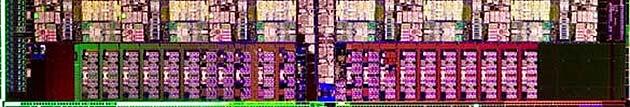
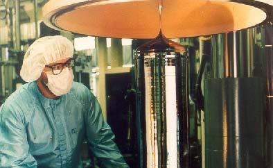
12 Intel Core i7 980X 32 nm ATV 2011, L1, Per Larsson-Edefors Page 23 Wafer Production ATV 2011, L1, Per Larsson-Edefors Page 24 12


13 Crystal Orientation Matter ATV 2011, L1, Per Larsson-Edefors Page 25 Lithography for IC ATV 2011, L1, Per Larsson-Edefors Page 26 13
. Numerical apertures exceeding 1.")

14 Lithography Challenge Speed! Exposure via mask reticle; stepper defines dies. Argon fluoride excimer laser at 193-nm wavelength. Absorption edge of air is at 185 nm. Optical proximity correction (for increasing #mask layers). Numerical apertures exceeding 1.0 possible via immersion in water. Double patterning. Future: EUV litho? Light sources? Mirrors? Vacuum? Keep an eye on Intel Fab 42, Chandler, AZ. ATV 2011, L1, Per Larsson-Edefors Page 27 Double Patterning Line density is an issue. Line width is not. Double patterning using space walls. ATV 2011, L1, Per Larsson-Edefors Page 28 14
. Metal gates to avoid gate polydepletion.")
 silicon for mobility enhancement. What will happen in multi-gate FETs?")
.")
15 Scaled MOSFETs High-k gate dielectric allows electric oxide thickness (EOT) scaling; avoids tunneling. (C = k A/T, where k = ε). Metal gates to avoid gate polydepletion. Work function regulation / V T tuning difficult. Strained (Ge) silicon for mobility enhancement. What will happen in multi-gate FETs? But still the MOSFET channel is poorly controlled, leading to substantial subthreshold leakage (and SCE). ATV 2011, L1, Per Larsson-Edefors Page 29 Small-Channel Effects (SCEs) ATV 2011, L1, Per Larsson-Edefors Page 30 15
16 Interconnects Performance bottleneck via long RC constants. Lateral dimensions shrink => stack of 10 layers progressively sized. Vertical dimensions cannot shrink as R increases too fast. Low-k dielectric for metal stack; starting to enter pre-metal layer too. All copper layers in processors. Copper bottom layer, with aluminum layers on top in e.g. DRAMs. In view of performance and yield, 3D makes sense ATV 2011, L1, Per Larsson-Edefors Page 31 ATV 2011 ATV 2011, L1, Per Larsson-Edefors Page 32 16
17 Organization September October cu. Several topics: Self study. Initial paper/book. Seminar. ATV 2011, L1, Per Larsson-Edefors Page 33 Next Meeting Friday Sep 16; 13.30? Topic defined (1 page). Expect some help from instructor (away Mon-Wed). No significant topic overlaps allowed. Bring calendar; more meetings scheduled. chalmers se/~perla/grad/atv/ You have to make yourself known; me name and personnummer. ATV 2011, L1, Per Larsson-Edefors Page 34 17
18 Topics Study + Seminar Alen - 3D chip integration Angelos - Volatile 3D memory technologies Dmitry - Non-volatile memory technologies Kasyab - Memristor technology Erik - On-chip optical interconnects Tung FinFETsFET Anurag - 14 nm fabrication ATV 2011, L1, Per Larsson-Edefors Page 35 18
Chapter 3: Basics Semiconductor Devices and Processing 2006/9/27 1. Topics
 Chapter 3: Basics Semiconductor Devices and Processing 2006/9/27 1 Topics What is semiconductor Basic semiconductor devices Basics of IC processing CMOS technologies 2006/9/27 2 1 What is Semiconductor
ECE 5745 Complex Digital ASIC Design Topic 2: CMOS Devices
 ECE 5745 Complex Digital ASIC Design Topic 2: CMOS Devices Christopher Batten School of Electrical and Computer Engineering Cornell University http://www.csl.cornell.edu/courses/ece5950 Simple Transistor
Chapter 3 Basics Semiconductor Devices and Processing
 Chapter 3 Basics Semiconductor Devices and Processing 1 Objectives Identify at least two semiconductor materials from the periodic table of elements List n-type and p-type dopants Describe a diode and
420 Intro to VLSI Design
 Dept of Electrical and Computer Engineering 420 Intro to VLSI Design Lecture 0: Course Introduction and Overview Valencia M. Joyner Spring 2005 Getting Started Syllabus About the Instructor Labs, Problem
MICROPROCESSOR TECHNOLOGY
 MICROPROCESSOR TECHNOLOGY Assis. Prof. Hossam El-Din Moustafa Lecture 3 Ch.1 The Evolution of The Microprocessor 17-Feb-15 1 Chapter Objectives Introduce the microprocessor evolution from transistors to
Advanced Digital Integrated Circuits. Lecture 2: Scaling Trends. Announcements. No office hour next Monday. Extra office hour Tuesday 2-3pm
 EE241 - Spring 20 Advanced Digital Integrated Circuits Lecture 2: Scaling Trends and Features of Modern Technologies Announcements No office hour next Monday Extra office hour Tuesday 2-3pm 2 1 Outline
Newer process technology (since 1999) includes :
 includes :") Newer process technology (since 1999) includes : copper metalization hi-k dielectrics for gate insulators si on insulator strained silicon lo-k dielectrics for interconnects Immersion lithography for masks
Newer process technology (since 1999) includes : copper metalization hi-k dielectrics for gate insulators si on insulator strained silicon lo-k dielectrics for interconnects Immersion lithography for masks
VLSI Design. Introduction
 Tassadaq Hussain VLSI Design Introduction Outcome of this course Problem Aims Objectives Outcomes Data Collection Theoretical Model Mathematical Model Validate Development Analysis and Observation Pseudo
VLSI Design. Introduction
 VLSI Design Introduction Outline Introduction Silicon, pn-junctions and transistors A Brief History Operation of MOS Transistors CMOS circuits Fabrication steps for CMOS circuits Introduction Integrated
Student Lecture by: Giangiacomo Groppi Joel Cassell Pierre Berthelot September 28 th 2004
 Student Lecture by: Giangiacomo Groppi Joel Cassell Pierre Berthelot September 28 th 2004 Lecture outline Historical introduction Semiconductor devices overview Bipolar Junction Transistor (BJT) Field
Basic Fabrication Steps
 Basic Fabrication Steps and Layout Somayyeh Koohi Department of Computer Engineering Adapted with modifications from lecture notes prepared by author Outline Fabrication steps Transistor structures Transistor
+1 (479)
") Introduction to VLSI Design http://csce.uark.edu +1 (479) 575-6043 yrpeng@uark.edu Invention of the Transistor Vacuum tubes ruled in first half of 20th century Large, expensive, power-hungry, unreliable
Introduction to VLSI Design http://csce.uark.edu +1 (479) 575-6043 yrpeng@uark.edu Invention of the Transistor Vacuum tubes ruled in first half of 20th century Large, expensive, power-hungry, unreliable
Sub-micron technology IC fabrication process trends SOI technology. Development of CMOS technology. Technology problems due to scaling
 Goodbye Microelectronics Welcome Nanoelectronics Sub-micron technology IC fabrication process trends SOI technology SiGe Tranzistor in 50nm process Virus The thickness of gate oxide= 1.2 nm!!! Today we
Lecture 4 -- Tuesday, Sept. 19: Non-uniform injection and/or doping. Diffusion. Continuity/conservation. The five basic equations.
 6.012 ELECTRONIC DEVICES AND CIRCUITS Schedule -- Fall 1995 (8/31/95 version) Recitation 1 -- Wednesday, Sept. 6: Review of 6.002 models for BJT. Discussion of models and modeling; motivate need to go
MSE 410/ECE 340: Electrical Properties of Materials Fall 2016 Micron School of Materials Science and Engineering Boise State University
 MSE 410/ECE 340: Electrical Properties of Materials Fall 2016 Micron School of Materials Science and Engineering Boise State University Practice Final Exam 1 Read the questions carefully Label all figures
EE241 - Spring 2013 Advanced Digital Integrated Circuits. Announcements. Sign up for Piazza if you haven t already
 EE241 - Spring 2013 Advanced Digital Integrated Circuits Lecture 2: Scaling Trends and Features of Modern Technologies Announcements Sign up for Piazza if you haven t already 2 1 Assigned Reading R.H.
Davinci. Semiconductor Device Simulaion in 3D SYSTEMS PRODUCTS LOGICAL PRODUCTS PHYSICAL IMPLEMENTATION SIMULATION AND ANALYSIS LIBRARIES TCAD
 SYSTEMS PRODUCTS LOGICAL PRODUCTS PHYSICAL IMPLEMENTATION SIMULATION AND ANALYSIS LIBRARIES TCAD Aurora DFM WorkBench Davinci Medici Raphael Raphael-NES Silicon Early Access TSUPREM-4 Taurus-Device Taurus-Lithography
Lecture 0: Introduction
 Lecture 0: Introduction Introduction Integrated circuits: many transistors on one chip. Very Large Scale Integration (VLSI): bucketloads! Complementary Metal Oxide Semiconductor Fast, cheap, low power
EE 5611 Introduction to Microelectronic Technologies Fall Thursday, September 04, 2014 Lecture 02
 EE 5611 Introduction to Microelectronic Technologies Fall 2014 Thursday, September 04, 2014 Lecture 02 1 Lecture Outline Review on semiconductor materials Review on microelectronic devices Example of microelectronic
Università degli Studi di Roma Tor Vergata Dipartimento di Ingegneria Elettronica. Analogue Electronics. Paolo Colantonio A.A.
 Università degli Studi di Roma Tor Vergata Dipartimento di Ingegneria Elettronica Analogue Electronics Paolo Colantonio A.A. 2015-16 Introduction: materials Conductors e.g. copper or aluminum have a cloud
The future of lithography and its impact on design
 The future of lithography and its impact on design Chris Mack www.lithoguru.com 1 Outline History Lessons Moore s Law Dennard Scaling Cost Trends Is Moore s Law Over? Litho scaling? The Design Gap The
Lecture: Integration of silicon photonics with electronics. Prepared by Jean-Marc FEDELI CEA-LETI
 Lecture: Integration of silicon photonics with electronics Prepared by Jean-Marc FEDELI CEA-LETI Context The goal is to give optical functionalities to electronics integrated circuit (EIC) The objectives
CONTENTS. 2.2 Schrodinger's Wave Equation 31. PART I Semiconductor Material Properties. 2.3 Applications of Schrodinger's Wave Equation 34
 CONTENTS Preface x Prologue Semiconductors and the Integrated Circuit xvii PART I Semiconductor Material Properties CHAPTER 1 The Crystal Structure of Solids 1 1.0 Preview 1 1.1 Semiconductor Materials
LEDs, Photodetectors and Solar Cells
 LEDs, Photodetectors and Solar Cells Chapter 7 (Parker) ELEC 424 John Peeples Why the Interest in Photons? Answer: Momentum and Radiation High electrical current density destroys minute polysilicon and
Department of Electrical Engineering IIT Madras
 Department of Electrical Engineering IIT Madras Sample Questions on Semiconductor Devices EE3 applicants who are interested to pursue their research in microelectronics devices area (fabrication and/or
Progress due to: Feature size reduction - 0.7X/3 years (Moore s Law). Increasing chip size - 16% per year. Creativity in implementing functions.
. Increasing chip size - 16% per year. Creativity in implementing functions.") Introduction - Chapter 1 Evolution of IC Fabrication 1960 and 1990 integrated t circuits. it Progress due to: Feature size reduction - 0.7X/3 years (Moore s Law). Increasing chip size - 16% per year. Creativity
Introduction - Chapter 1 Evolution of IC Fabrication 1960 and 1990 integrated t circuits. it Progress due to: Feature size reduction - 0.7X/3 years (Moore s Law). Increasing chip size - 16% per year. Creativity
NAME: Last First Signature
 UNIVERSITY OF CALIFORNIA, BERKELEY College of Engineering Department of Electrical Engineering and Computer Sciences EE 130: IC Devices Spring 2003 FINAL EXAMINATION NAME: Last First Signature STUDENT
PHYSICS OF SEMICONDUCTOR DEVICES
 PHYSICS OF SEMICONDUCTOR DEVICES PHYSICS OF SEMICONDUCTOR DEVICES by J. P. Colinge Department of Electrical and Computer Engineering University of California, Davis C. A. Colinge Department of Electrical
EE4800 CMOS Digital IC Design & Analysis. Lecture 1 Introduction Zhuo Feng
 EE4800 CMOS Digital IC Design & Analysis Lecture 1 Introduction Zhuo Feng 1.1 Prof. Zhuo Feng Office: EERC 730 Phone: 487-3116 Email: zhuofeng@mtu.edu Class Website http://www.ece.mtu.edu/~zhuofeng/ee4800fall2010.html
Electronics The basics of semiconductor physics
 Electronics The basics of semiconductor physics Prof. Márta Rencz, Gábor Takács BME DED 17/09/2015 1 / 37 The basic properties of semiconductors Range of conductivity [Source: http://www.britannica.com]
Electronic devices-i. Difference between conductors, insulators and semiconductors
 Electronic devices-i Semiconductor Devices is one of the important and easy units in class XII CBSE Physics syllabus. It is easy to understand and learn. Generally the questions asked are simple. The unit
FUNDAMENTALS OF MODERN VLSI DEVICES
 19-13- FUNDAMENTALS OF MODERN VLSI DEVICES YUAN TAUR TAK H. MING CAMBRIDGE UNIVERSITY PRESS Physical Constants and Unit Conversions List of Symbols Preface page xi xiii xxi 1 INTRODUCTION I 1.1 Evolution
SRM INSTITUTE OF SCIENCE AND TECHNOLOGY (DEEMED UNIVERSITY)
") SRM INSTITUTE OF SCIENCE AND TECHNOLOGY (DEEMED UNIVERSITY) QUESTION BANK I YEAR B.Tech (II Semester) ELECTRONIC DEVICES (COMMON FOR EC102, EE104, IC108, BM106) UNIT-I PART-A 1. What are intrinsic and
SRM INSTITUTE OF SCIENCE AND TECHNOLOGY (DEEMED UNIVERSITY) QUESTION BANK I YEAR B.Tech (II Semester) ELECTRONIC DEVICES (COMMON FOR EC102, EE104, IC108, BM106) UNIT-I PART-A 1. What are intrinsic and
Lecture 1 Introduction to Solid State Electronics
 EE 471: Transport Phenomena in Solid State Devices Spring 2018 Lecture 1 Introduction to Solid State Electronics Bryan Ackland Department of Electrical and Computer Engineering Stevens Institute of Technology
Intel's 65 nm Logic Technology Demonstrated on 0.57 µm 2 SRAM Cells
 Intel's 65 nm Logic Technology Demonstrated on 0.57 µm 2 SRAM Cells Mark Bohr Intel Senior Fellow Director of Process Architecture & Integration Intel 1 What are We Announcing? Intel has fabricated fully-functional
Lecture #29. Moore s Law
 Lecture #29 ANNOUNCEMENTS HW#15 will be for extra credit Quiz #6 (Thursday 5/8) will include MOSFET C-V No late Projects will be accepted after Thursday 5/8 The last Coffee Hour will be held this Thursday
IC Knowledge LLC, PO Box 20, Georgetown, MA Ph: (978) , Fx: (978)
 , Fx: (978)") IC Knowledge LLC, PO Box 20, Georgetown, MA 01833 www.icknowledge.com Ph: (978) 352 7610, Fx: (978) 352 3870 Linx Consulting, PO Box 384, Mendon, MA 01756 0384 www.linxconsulting.com Ph: (617) 273 8837
IC Knowledge LLC, PO Box 20, Georgetown, MA 01833 www.icknowledge.com Ph: (978) 352 7610, Fx: (978) 352 3870 Linx Consulting, PO Box 384, Mendon, MA 01756 0384 www.linxconsulting.com Ph: (617) 273 8837
Electronic Circuits I. Instructor: Dr. Alaa Mahmoud
 Electronic Circuits I Instructor: Dr. Alaa Mahmoud alaa_y_emam@hotmail.com Chapter 27 Diode and diode application Outline: Semiconductor Materials The P-N Junction Diode Biasing P-N Junction Volt-Ampere
ECE520 VLSI Design. Lecture 2: Basic MOS Physics. Payman Zarkesh-Ha
 ECE520 VLSI Design Lecture 2: Basic MOS Physics Payman Zarkesh-Ha Office: ECE Bldg. 230B Office hours: Wednesday 2:00-3:00PM or by appointment E-mail: pzarkesh@unm.edu Slide: 1 Review of Last Lecture Semiconductor
CMOS Digital Integrated Circuits Lec 2 Fabrication of MOSFETs
 CMOS Digital Integrated Circuits Lec 2 Fabrication of MOSFETs 1 CMOS Digital Integrated Circuits 3 rd Edition Categories of Materials Materials can be categorized into three main groups regarding their
Transistor was first invented by William.B.Shockley, Walter Brattain and John Bardeen of Bell Labratories. In 1961, first IC was introduced.
 Unit 1 Basic MOS Technology Transistor was first invented by William.B.Shockley, Walter Brattain and John Bardeen of Bell Labratories. In 1961, first IC was introduced. Levels of Integration:- i) SSI:-
Downloaded from
 Question 14.1: In an n-type silicon, which of the following statement is true: (a) Electrons are majority carriers and trivalent atoms are the dopants. (b) Electrons are minority carriers and pentavalent
Fin-Shaped Field Effect Transistor (FinFET) Min Ku Kim 03/07/2018
 Min Ku Kim 03/07/2018") Fin-Shaped Field Effect Transistor (FinFET) Min Ku Kim 03/07/2018 ECE 658 Sp 2018 Semiconductor Materials and Device Characterizations OUTLINE Background FinFET Future Roadmap Keeping up w/ Moore s Law
Fin-Shaped Field Effect Transistor (FinFET) Min Ku Kim 03/07/2018 ECE 658 Sp 2018 Semiconductor Materials and Device Characterizations OUTLINE Background FinFET Future Roadmap Keeping up w/ Moore s Law
Chapter Semiconductor Electronics
 Chapter Semiconductor Electronics Q1. p-n junction is said to be forward biased, when [1988] (a) the positive pole of the battery is joined to the p- semiconductor and negative pole to the n- semiconductor
Photolithography I ( Part 1 )
") 1 Photolithography I ( Part 1 ) Chapter 13 : Semiconductor Manufacturing Technology by M. Quirk & J. Serda Bjørn-Ove Fimland, Department of Electronics and Telecommunication, Norwegian University of Science
1 Photolithography I ( Part 1 ) Chapter 13 : Semiconductor Manufacturing Technology by M. Quirk & J. Serda Bjørn-Ove Fimland, Department of Electronics and Telecommunication, Norwegian University of Science
Integrated diodes. The forward voltage drop only slightly depends on the forward current. ELEKTRONIKOS ĮTAISAI
 1 Integrated diodes pn junctions of transistor structures can be used as integrated diodes. The choice of the junction is limited by the considerations of switching speed and breakdown voltage. The forward
value of W max for the device. The at band voltage is -0.9 V. Problem 5: An Al-gate n-channel MOS capacitor has a doping of N a = cm ;3. The oxi
 Prof. Jasprit Singh Fall 2001 EECS 320 Homework 10 This homework is due on December 6 Problem 1: An n-type In 0:53 Ga 0:47 As epitaxial layer doped at 10 16 cm ;3 is to be used as a channel in a FET. A
Lecture Notes 5 CMOS Image Sensor Device and Fabrication
 Lecture Notes 5 CMOS Image Sensor Device and Fabrication CMOS image sensor fabrication technologies Pixel design and layout Imaging performance enhancement techniques Technology scaling, industry trends
Notes. (Subject Code: 7EC5)
") COMPUCOM INSTITUTE OF TECHNOLOGY & MANAGEMENT, JAIPUR (DEPARTMENT OF ELECTRONICS & COMMUNICATION) Notes VLSI DESIGN NOTES (Subject Code: 7EC5) Prepared By: MANVENDRA SINGH Class: B. Tech. IV Year, VII
COMPUCOM INSTITUTE OF TECHNOLOGY & MANAGEMENT, JAIPUR (DEPARTMENT OF ELECTRONICS & COMMUNICATION) Notes VLSI DESIGN NOTES (Subject Code: 7EC5) Prepared By: MANVENDRA SINGH Class: B. Tech. IV Year, VII
Semiconductor Physics and Devices
 Metal-Semiconductor and Semiconductor Heterojunctions The Metal-Oxide-Semiconductor Field-Effect Transistor (MOSFET) is one of two major types of transistors. The MOSFET is used in digital circuit, because
Lecture 4 - Digital Representations III + Transistors
 Lecture 4 - Digital Representations III + Transistors Video: Seems like a natural extension from images no? We just have a new dimension (time) Each frame is just an image made up of pixels Display n frames
Intrinsic Semiconductor
 Semiconductors Crystalline solid materials whose resistivities are values between those of conductors and insulators. Good electrical characteristics and feasible fabrication technology are some reasons
Lecture Wrap up. December 13, 2005
 6.012 Microelectronic Devices and Circuits Fall 2005 Lecture 26 1 Lecture 26 6.012 Wrap up December 13, 2005 Contents: 1. 6.012 wrap up Announcements: Final exam TA review session: December 16, 7:30 9:30
 Energy band diagrams Metals: 9. ELECTRONIC DEVICES GIST ρ= 10-2 to 10-8 Ω m Insulators: ρ> 10 8 Ω m Semiconductors ρ= 1 to 10 5 Ω m 109 A. Intrinsic semiconductors At T=0k it acts as insulator At room
Transistor Scaling in the Innovation Era. Mark Bohr Intel Senior Fellow Logic Technology Development August 15, 2011
 Transistor Scaling in the Innovation Era Mark Bohr Intel Senior Fellow Logic Technology Development August 15, 2011 MOSFET Scaling Device or Circuit Parameter Scaling Factor Device dimension tox, L, W
EMT 251 Introduction to IC Design
 EMT 251 Introduction to IC Design (Pengantar Rekabentuk Litar Terkamir) Semester II 2011/2012 Introduction to IC design and Transistor Fundamental Some Keywords! Very-large-scale-integration (VLSI) is
Comparative Study of Silicon and Germanium Doping-less Tunnel Field Effect Transistors
 IJSTE - International Journal of Science Technology & Engineering Volume 2 Issue 5 November 2015 ISSN (online): 2349-784X Comparative Study of Silicon and Germanium Doping-less Tunnel Field Effect Transistors
Basic concepts. Optical Sources (b) Optical Sources (a) Requirements for light sources (b) Requirements for light sources (a)
 Optical Sources (a) Requirements for light sources (b) Requirements for light sources (a)") Optical Sources (a) Optical Sources (b) The main light sources used with fibre optic systems are: Light-emitting diodes (LEDs) Semiconductor lasers (diode lasers) Fibre laser and other compact solid-state
Optical Sources (a) Optical Sources (b) The main light sources used with fibre optic systems are: Light-emitting diodes (LEDs) Semiconductor lasers (diode lasers) Fibre laser and other compact solid-state
EECS 151/251A Spring 2019 Digital Design and Integrated Circuits. Instructors: Wawrzynek. Lecture 8 EE141
 EECS 151/251A Spring 2019 Digital Design and Integrated Circuits Instructors: Wawrzynek Lecture 8 EE141 From the Bottom Up IC processing CMOS Circuits (next lecture) EE141 2 Overview of Physical Implementations
HOW TO CONTINUE COST SCALING. Hans Lebon
 HOW TO CONTINUE COST SCALING Hans Lebon OUTLINE Scaling & Scaling Challenges Imec Technology Roadmap Wafer size scaling : 450 mm 2 COST SCALING IMPROVED PERFORMANCE 3 GLOBAL TRAFFIC FORECAST Cloud Traffic
Digital Integrated Circuits
 Digital Integrated Circuits Yaping Dan ( 但亚平 ), PhD Office: Law School North 301 Tel: 34206045-3011 Email: yapingd@gmail.com Digital Integrated Circuits Introduction p-n junctions and MOSFETs The CMOS
CHAPTER FORMULAS & NOTES
 Formulae For u SEMICONDUCTORS By Mir Mohammed Abbas II PCMB 'A' 1 Important Terms, Definitions & Formulae CHAPTER FORMULAS & NOTES 1 Intrinsic Semiconductor: The pure semiconductors in which the electrical
Chapter 1. Introduction
 Chapter 1 Introduction 1.1 Introduction of Device Technology Digital wireless communication system has become more and more popular in recent years due to its capability for both voice and data communication.
450mm and Moore s Law Advanced Packaging Challenges and the Impact of 3D
 450mm and Moore s Law Advanced Packaging Challenges and the Impact of 3D Doug Anberg VP, Technical Marketing Ultratech SOKUDO Lithography Breakfast Forum July 10, 2013 Agenda Next Generation Technology
Alternatives to standard MOSFETs. What problems are we really trying to solve?
 Alternatives to standard MOSFETs A number of alternative FET schemes have been proposed, with an eye toward scaling up to the 10 nm node. Modifications to the standard MOSFET include: Silicon-in-insulator
Downloaded from
 SOLID AND SEMICONDUCTOR DEVICES (EASY AND SCORING TOPIC) 1. Distinction of metals, semiconductor and insulator on the basis of Energy band of Solids. 2. Types of Semiconductor. 3. PN Junction formation
SEMICONDUCTOR ELECTRONICS: MATERIALS, DEVICES AND SIMPLE CIRCUITS. Class XII : PHYSICS WORKSHEET
 SEMICONDUCT ELECTRONICS: MATERIALS, DEVICES AND SIMPLE CIRCUITS Class XII : PHYSICS WKSHEET 1. How is a n-p-n transistor represented symbolically? (1) 2. How does conductivity of a semiconductor change
Innovation to Advance Moore s Law Requires Core Technology Revolution
 Innovation to Advance Moore s Law Requires Core Technology Revolution Klaus Schuegraf, Ph.D. Chief Technology Officer Silicon Systems Group Applied Materials UC Berkeley Seminar March 9 th, 2012 Innovation
Semiconductor Memory: DRAM and SRAM. Department of Electrical and Computer Engineering, National University of Singapore
 Semiconductor Memory: DRAM and SRAM Outline Introduction Random Access Memory (RAM) DRAM SRAM Non-volatile memory UV EPROM EEPROM Flash memory SONOS memory QD memory Introduction Slow memories Magnetic
Sharjah Indian School, Sharjah ELECTRONIC DEVICES - Class XII (Boys Wing) Page 01
 Page 01") ELECTRONIC DEVICES - Class XII (Boys Wing) Page 01 Electronics is the fast developing branch of Physics. Before the discovery of transistors in 1948, vacuum tubes (thermionic valves) were used as the building
ELECTRONIC DEVICES - Class XII (Boys Wing) Page 01 Electronics is the fast developing branch of Physics. Before the discovery of transistors in 1948, vacuum tubes (thermionic valves) were used as the building
Atoms and Valence Electrons
 Technology Overview Atoms and Valence Electrons Conduc:on and Valence Bands Energy Band Gaps in Materials Band gap N- type and P- type Doping Silicon and Adjacent Atoms PN Junc:on Forward Biased PN Junc:on
Introduction to Electronic Devices
 (Course Number 300331) Fall 2006 Instructor: Dr. Dietmar Knipp Assistant Professor of Electrical Engineering Information: http://www.faculty.iubremen.de/dknipp/ Source: Apple Ref.: Apple Ref.: IBM Critical
Semiconductor Devices
 Semiconductor Devices Modelling and Technology Source Electrons Gate Holes Drain Insulator Nandita DasGupta Amitava DasGupta SEMICONDUCTOR DEVICES Modelling and Technology NANDITA DASGUPTA Professor Department
ISSCC 2003 / SESSION 1 / PLENARY / 1.1
 ISSCC 2003 / SESSION 1 / PLENARY / 1.1 1.1 No Exponential is Forever: But Forever Can Be Delayed! Gordon E. Moore Intel Corporation Over the last fifty years, the solid-state-circuits industry has grown
EE301 Electronics I , Fall
 EE301 Electronics I 2018-2019, Fall 1. Introduction to Microelectronics (1 Week/3 Hrs.) Introduction, Historical Background, Basic Consepts 2. Rewiev of Semiconductors (1 Week/3 Hrs.) Semiconductor materials
Microelectronics, BSc course
 Microelectronics, BSc course MOS circuits: CMOS circuits, construction http://www.eet.bme.hu/~poppe/miel/en/14-cmos.pptx http://www.eet.bme.hu The abstraction level of our study: SYSTEM + MODULE GATE CIRCUIT
PHYS 3050 Electronics I
 PHYS 3050 Electronics I Chapter 4. Semiconductor Diodes and Transistors Earth, Moon, Mars, and Beyond Dr. Jinjun Shan, Associate Professor of Space Engineering Department of Earth and Space Science and
EE669: VLSI TECHNOLOGY
 EE669: VLSI TECHNOLOGY Autumn Semester Graduate Course 2014-2015 Session by Arun N. Chandorkar Emeritus Fellow Professor Department of Electrical Engineering Indian Institute of Technology, Bombay Powai,
ELECTRONIC DEVICES AND CIRCUITS
 ELECTRONIC DEVICES AND CIRCUITS 1. At room temperature the current in an intrinsic semiconductor is due to A. holes B. electrons C. ions D. holes and electrons 2. Work function is the maximum energy required
Chapter 2 : Semiconductor Materials & Devices (II) Feb
 Feb") Chapter 2 : Semiconductor Materials & Devices (II) 1 Reference 1. SemiconductorManufacturing Technology: Michael Quirk and Julian Serda (2001) 3. Microelectronic Circuits (5/e): Sedra & Smith (2004) 4.
Chapter 2 : Semiconductor Materials & Devices (II) 1 Reference 1. SemiconductorManufacturing Technology: Michael Quirk and Julian Serda (2001) 3. Microelectronic Circuits (5/e): Sedra & Smith (2004) 4.
Introduction to Materials Engineering: Materials Driving the Electronics Revolution Robert Hull, MSE
 Introduction to Materials Engineering: Materials Driving the Electronics Revolution Robert Hull, MSE Outline Microelectronics Miniaturization Historical Development: Electronics before Semiconductors The
FABRICATION OF CMOS INTEGRATED CIRCUITS. Dr. Mohammed M. Farag
 FABRICATION OF CMOS INTEGRATED CIRCUITS Dr. Mohammed M. Farag Outline Overview of CMOS Fabrication Processes The CMOS Fabrication Process Flow Design Rules Reference: Uyemura, John P. "Introduction to
ITRS MOSFET Scaling Trends, Challenges, and Key Technology Innovations
 Workshop on Frontiers of Extreme Computing Santa Cruz, CA October 24, 2005 ITRS MOSFET Scaling Trends, Challenges, and Key Technology Innovations Peter M. Zeitzoff Outline Introduction MOSFET scaling and
Module-3: Metal Oxide Semiconductor (MOS) & Emitter coupled logic (ECL) families
 & Emitter coupled logic (ECL) families") 1 Module-3: Metal Oxide Semiconductor (MOS) & Emitter coupled logic (ECL) families 1. Introduction 2. Metal Oxide Semiconductor (MOS) logic 2.1. Enhancement and depletion mode 2.2. NMOS and PMOS inverter
1 Module-3: Metal Oxide Semiconductor (MOS) & Emitter coupled logic (ECL) families 1. Introduction 2. Metal Oxide Semiconductor (MOS) logic 2.1. Enhancement and depletion mode 2.2. NMOS and PMOS inverter
UNIT IX ELECTRONIC DEVICES
 UNT X ELECTRONC DECES Weightage Marks : 07 Semiconductors Semiconductors diode-- characteristics in forward and reverse bias, diode as rectifier. - characteristics of LED, Photodiodes, solarcell and Zener
ENG2410 Digital Design CMOS Technology. Fall 2017 S. Areibi School of Engineering University of Guelph
 ENG2410 Digital Design CMOS Technology Fall 2017 S. reibi School of Engineering University of Guelph The Transistor Revolution First transistor Bell Labs, 1948 Bipolar logic 1960 s Intel 4004 processor
VALLIAMMAI ENGINEERING COLLEGE SRM Nagar, Kattankulathur
 VALLIAMMAI ENGINEERING COLLEGE SRM Nagar, Kattankulathur 603 203. DEPARTMENT OF ELECTRONICS & COMMUNICATION ENGINEERING SUBJECT QUESTION BANK : EC6201 ELECTRONIC DEVICES SEM / YEAR: II / I year B.E.ECE
Assoc. Prof. Dr. MONTREE SIRIPRUCHYANUN
 1 Assoc. Prof. Dr. MONTREE SIRIPRUCHYANUN Dept. of Teacher Training in Electrical Engineering 1 King Mongkut s Institute of Technology North Bangkok 1929 Bulky, expensive and required high supply voltages.
Integrated Circuit Technology (Course Code: EE662) Lecture 1: Introduction
 Lecture 1: Introduction") Indian Institute of Technology Jodhpur, Year 2015 2016 Integrated Circuit Technology (Course Code: EE662) Lecture 1: Introduction Course Instructor: Shree Prakash Tiwari, Ph.D. Email: sptiwari@iitj.ac.in
Indian Institute of Technology Jodhpur, Year 2015 2016 Integrated Circuit Technology (Course Code: EE662) Lecture 1: Introduction Course Instructor: Shree Prakash Tiwari, Ph.D. Email: sptiwari@iitj.ac.in
Semiconductor Lasers Semiconductors were originally pumped by lasers or e-beams First diode types developed in 1962: Create a pn junction in
 Semiconductor Lasers Semiconductors were originally pumped by lasers or e-beams First diode types developed in 1962: Create a pn junction in semiconductor material Pumped now with high current density
Reg. No. : Question Paper Code : B.E./B.Tech. DEGREE EXAMINATION, NOVEMBER/DECEMBER Second Semester
 WK 5 Reg. No. : Question Paper Code : 27184 B.E./B.Tech. DEGREE EXAMINATION, NOVEMBER/DECEMBER 2015. Time : Three hours Second Semester Electronics and Communication Engineering EC 6201 ELECTRONIC DEVICES
Design Simulation and Analysis of NMOS Characteristics for Varying Oxide Thickness
 MIT International Journal of Electronics and Communication Engineering, Vol. 4, No. 2, August 2014, pp. 81 85 81 Design Simulation and Analysis of NMOS Characteristics for Varying Oxide Thickness Alpana
INTRODUCTION TO MOS TECHNOLOGY
 INTRODUCTION TO MOS TECHNOLOGY 1. The MOS transistor The most basic element in the design of a large scale integrated circuit is the transistor. For the processes we will discuss, the type of transistor
CMOS Technology & Business Trends
 CMOS Technology & Business Trends Can the semiconductor industry afford to continue advancing? Peter M. O Neill Automated Test Innovations Agilent Laboratories Disclaimers Not a thoroughly researched paper
Session 10: Solid State Physics MOSFET
 Session 10: Solid State Physics MOSFET 1 Outline A B C D E F G H I J 2 MOSCap MOSFET Metal-Oxide-Semiconductor Field-Effect Transistor: Al (metal) SiO2 (oxide) High k ~0.1 ~5 A SiO2 A n+ n+ p-type Si (bulk)
Digital Electronics. By: FARHAD FARADJI, Ph.D. Assistant Professor, Electrical and Computer Engineering, K. N. Toosi University of Technology
 K. N. Toosi University of Technology Chapter 7. Field-Effect Transistors By: FARHAD FARADJI, Ph.D. Assistant Professor, Electrical and Computer Engineering, K. N. Toosi University of Technology http://wp.kntu.ac.ir/faradji/digitalelectronics.htm
Solid State Devices- Part- II. Module- IV
 Solid State Devices- Part- II Module- IV MOS Capacitor Two terminal MOS device MOS = Metal- Oxide- Semiconductor MOS capacitor - the heart of the MOSFET The MOS capacitor is used to induce charge at the
Optical Amplifiers. Continued. Photonic Network By Dr. M H Zaidi
 Optical Amplifiers Continued EDFA Multi Stage Designs 1st Active Stage Co-pumped 2nd Active Stage Counter-pumped Input Signal Er 3+ Doped Fiber Er 3+ Doped Fiber Output Signal Optical Isolator Optical
Mathematics and Science in Schools in Sub-Saharan Africa
 Mathematics and Science in Schools in Sub-Saharan Africa SEMICONDUCTORS What is a Semiconductor? What is a Semiconductor? Microprocessors LED Transistors Capacitors Range of Conduciveness The semiconductors
Semiconductor Process Reliability SVTW 2012 Esko Mikkola, Ph.D. & Andrew Levy
 Semiconductor Process Reliability SVTW 2012 Esko Mikkola, Ph.D. & Andrew Levy 1 IC Failure Modes Affecting Reliability Via/metallization failure mechanisms Electro migration Stress migration Transistor