Overview of technology for RF and Digital Optical Communications
|
|
|
- Lindsay Snow
- 6 years ago
- Views:
Transcription
1 Overview of technology for RF and Digital Optical Communications
2 Structure of talk Day 1 Introduction What is EPIC, How has EPIC evolved Use to show how a research and development capability matched to the targeted manufacturing capability helps reduce time to product. Where is EPIC today. Components etc How has EPIC IMPACTED Communications. (Bring in a CHIP to Pass Around.) Application to RF Communication Day 2 Application to Digital Optical Communications Future application to high capacity Analog to digital.

3 Electronic and Photonic Integrated Circuits (EPIC) Integrated Silicon Photonics involves the realization of optical functions on silicon chips with existing and future Silicon Microelectronic Technology. Has been studied actively since the early 1990 s Research has progressed however, efforts have been smaller than those in silicon micromechanics, and negligible (near zero) compared to silicon microelectronics. Recent work has for the first time applied a full CMOS foundry with its specialized equipment to the problem of Integrated Silicon Photonics. Has allowed us to apply large volume of existing Silicon Microelectronic research to the problem of ISP.
4 Why is Silicon Photonics important to Optical Communications? Integration of photonic components with CMOS electronics CMOS drivers, processors and digital electronic interfaces, Photonic filters, modulators, detectors, waveguides, splitters, optical switches. Size and Power reduction through scale reduction and device efficiency improvement. Lower optical losses, lower power consumption to achieve a specific index change etc. Allows the best of the electronic and photonic component functionality to be employed to demonstrate improved system performance. Integrated Photonic Platforms, In addition to being able to treat an Ultra Wide Band RF signal as an Ultra Narrow Signal, provide added efficiency in their ability to move signals around the chip and preserve their shape and phase.


5 What level of integration is possible and where? LEVEL 1 Die and Package Level Integration LEVEL 2 System level Integration LEVEL 3 Platform Level Integration Integration of Photonic based functions Intra chip optical data routing Application of RF functionality in optical domain Integration of Photonic and Electronic components within a single die Combination of photonic based functional components to build a usable system Photonic based communications, IW, EW, SIGNINT, ECM, and RADAR Photonically reconfigurable antennas Integration of photonic based systems and data links. Application of analog and digital photonic data links. Integration of photonic flight controls and interfaces.


6 HOW WILL THESE TECHNOLOGIES AFFECT FUTURE SYSTEMS AND PRODUCT DEVELOPMENT? CURRENT 0.18mm SOI CMOS HIC Silicon Waveguides Germanium Detectors Silicon Phase Modulators EVOLVING Integrated Optical Sources Integrated Optical Amplifiers
7 Technology: Why are we interested? On Chip optical routing and processing of RF and Microwave Signals is more efficient in terms of control of phase, loss and Size On Chip Signal fidelity Comparison TYPICAL CPW (1mm Thick, G.T. 150mm Wide) 2.0 db/cm, 18GHz BW 3mm Bend Radius (0.25 db/turn Loss) 0.50mm 0.25mm High Index Contrast Waveguide 0.35dB/cm, 100THz BW 1mm Bend Radius (0.1 db/turn Loss) Integrated Photonic Platforms, In addition to being able to treat an Ultra Wide Band RF signal as an Ultra Narrow Signal, provide added efficiency in their ability to move signals around the chip and preserve their shape and phase.


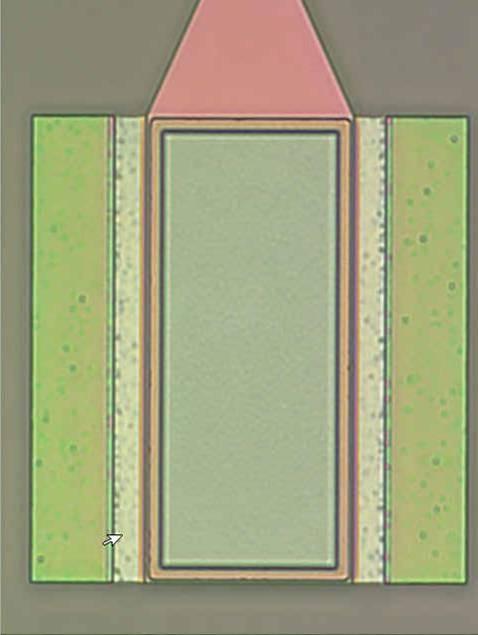
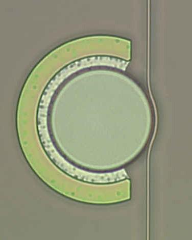
8 Examples of Integrated Devices. Segmented Path Optical Gyroscope Fabricated in our Silicon Photonic Process NIR Image of 1550nm modal propagation through lower coupler on our optical gyroscope Micrograph of Fabricated Gyroscope
9 Waveguide Modulator Detector nfet pfet MIM CAPACITOR Level of Integration Our Silicon Photonic work represents a new system of technologies that enable the monolithic fabrication of a wide range of photonic and electronic components. The Diagram at Right Shows the level of integration that will be included within our next process run PHOTONIC ELECTRONIC BOX 3.0 mm

 CMOS Electronics -20-30 Tuned output Fabricated High Index")
 Modulators -40 193.39 193.40 193.41 193.42 193.43 193.")
 and excellent out of band rejection (>45 db) Detectors 70.0µ 60.0µ 71mA photocurrent. 50.0µ 40.")
 ( Demonstrated Si ring modulators with lowest")
10 Photocurrent (A) Transmittance (db) Essential Components of our EPIC Technology Optical Waveguides Optical Filters SEM of a-si Waveguides Deposited Waveguide Micrograph of EPIC Filter In R R R R Oxide Underclad Passive output -10 (as fabricated) CMOS Electronics Tuned output Fabricated High Index Contrast waveguides in a rad-hard CMOS foundry with state of the art transmission losses (0.35 db/cm in SOI, 4 db/cm in a-si) Modulators Frequency (THz) Demonstrated fully tunable, integrated optical filters with fine passband resolution (0.6 GHz) and excellent out of band rejection (>45 db) Detectors 70.0µ 60.0µ 71mA photocurrent. 50.0µ 40.0µ 30.0µ 20.0µ Integrated SiGe waveguide detector 10.0µ Photodetector length mm) ( Demonstrated Si ring modulators with lowest reported power to date, <1.0 V at < 1 ma, and modulation speeds of > 6.5 Gbps Demonstrated discrete SiGe detectors with High responsivities and Bandwidths

11 Volts The E in EPIC The E18 Process has worked to demonstrate a stable process for electronic as well as photonic elements Have worked to turn our Rad Hard process into a Process Hard ONE To Date, within our photonic process, we have demonstrated functional: 0.18um N & P FETS capable of operation out to 20GHz 0.8 Bipolar Transistors A wide Range of Passives 0.5 RF waveguides 0.4 Lot NFET V T - linear Upper Spec Target Spec Lower Spec NFET test sites
12 The AS-EPIC Signal Processor Chip Objective To demonstrate the world s first densely integrated Application Specific Electronic Photonic Integrated Circuit (AS-EPIC). Demonstrate the meaningful integration of this technology into an existing product Approach Integrate the best technology to realize our AS-EPIC chip. This involves combining CMOS compatible, low loss, high index contrast (HIC) waveguides and optoelectronic components to form optical filters, modulators, and detectors with associated tuning, driver and TIA electronic circuits. 4.5X Increase IBW 95X Reduction Size 80X 4.5X Reduction Increase IBW in Weight 95X Reduction in Size Power 100X Reduction in Cost
13 Technology: Communications Impact? EPIC technology enable chip scale components that will revolutionize communications RF Communications EPIC Phase I Tunable RF Filter Monolithic: 54 optical elements Digital Optical Communications The integration of photonics and electronics will enable a new generation of inexpensive aerospace components: Digital channelizers for EW/IW systems Photonic beam forming (Butler Matrix) for Radar, MIMO, etc. Integrated laser gyroscope (smaller, lower cost, more accurate) Photo-RF data links for air and space platforms Optical communications (military and commercial- fiber to the home) Photonic clocking for microprocessors Document number 13
14 EPIC Chip Design Elements The BAE SYSTEMS EPIC channelizer represented the most complex, integrated optical component in existence, (With the complication of electronics) The design on the following slides represents a chip with all filters required for an 18 GHz IBW device It embodied: 16 Optical Band Pass Filters (BPF) 32 Germanium Detectors (DET) w/ Integrated Transimpedance Amplifiers (TIA) 8 RF->Optical Modulators 1 Nulling Filter The chip will have integrated electronics to assist with filter control and tuning
15 Layout of the BAE SYSTEM EPIC Channelizer Band Pass Filter Detector ML LASER 2.5GHz Note: Laser 1* frequency is 625MHz Lower than Laser 2. Modulator Laser 1* Band 1 RF (0-10GHz) Laser 1 Band 1 RF (0-10GHz) Modulator Mod Driver Modulator Mod Driver Nulling Filter Control Nulling Filter BPF Control BPF BPF BPF Control BPF BPF BPF Det TIA BPF Det TIA BPF Det BPF Det BPF Det TIA BPF Det TIA BPF Det TIA BPF Det TIA TIA TIA BPF Det TIA BPF Det TIA BPF Det BPF Det Det Det TIA TIA Det Det TIA TIA TIA TIA Band 1 Odd Channels Transimpedance Amplifier Band 1 Even Channels

16 Overview of EPIC RFChannelizer Most Recent BAE SYSTEMS EPIC chip, embodies Electro and Thermo-optic phase control, low loss waveguides, Detectors, Digital CMOS, RF CMOS and Analog CMOS (for control of Thermo-optic devices.)


17 Optical In RF OUT Integration of Germanium Photodiodes with High Speed TIA Balanced Germanium Photodiodes Trans-impedance Amplifier

18 EPIC integrated 0-20GHz Cascaded Modulator Driver Using BAE SYSTEMS EPIC technology 4 types electronic circuitry were successfully integrated: Digital CMOS in the control circuitry (addressing, latching, etc.) Low power precision analog in the DAC circuitry High power analog in the tuning High Frequency analog in the modulator drivers and TIA s document number 18
19 Devices and There Applications
20 Basics of the ISP technologies Technology involving the generation, conduction, manipulation and detection of light in a well defined densely integrated fashion on silicon. Electrons and photons are the basic functional units of electronic and photonics. Electrons propagate along regions of high electrical conductivity, Photons propagate along regions having a high refractive index variation. Photonic waveguides correspond to electrical wires, propagating light from one point to another. Optoelectronic components, such as lasers, detectors, and modulators act as a bridge between photonic and electronic signals Optical amplification boosts attenuated optical signals Compensates for the losses associated with non-ideal components and power splitters. Future Optical transistors and other all-optical components based on nonlinear phenomena will enable extremely fast optical computing, interfacing, and all-optical fiber communications
21 Silicon Waveguides While at visible wavelengths from 200 to 700 nm, Si is highly transparent at near-ir wavelengths from 1.2 to approximately 7 µm Particularly useful as fiber-optic communication, which is usually carried out between 1.3 and 1.7 µm, and especially at λ 1.55 µm has initiated and supported the development of a wide range of critical components such as optical sources, amplifiers, modulators and detectors. Light propagation in a silicon waveguide is based on total internal reflection (TIR) at the outer boundaries of the Si core. The core index n Si 3.45 is surrounded by SiO 2 (n ) the index difference n = n Si - n 0 = 2 Extremely high compared to other waveguide technologies and optical fibers ( n < 0.01).
22 Basic Silicon HIC Waveguide fabrication Key fabrication challenges: Deposition, Etching, Polishing Surface Roughness top & bottom Sidewall Roughness Si SiO2 Silicon Substrate


23 Silicon Waveguide fabrication efficiency Application of CMOS fabrication methodology has numerous advantages, including the lowest possible periodic variation in the sidewall though application of statistically verified process steps. New Waveguide hard mask etch techniques reduce roughness by 30% over reported values, demonstrated unprecedented device uniformity. Hard Mask Si SiO 2 Ridge Waveguide Channel Waveguide

24 Silicon Waveguide fabrication efficiency

 in order to maximize the aforementioned overlap, increasing the effective index change.")
25 Physical implementation of Modulator Technology in the EPIC Fabrication Platform, individual modulator technologies Thermo-optic Phase Modulator The refractive Index variation of silicon due to the thermo-optic effect is given by: 1. 86x10 T n 4 MOS based EO Modulator Bias applied across a gate oxide over the modulator induces an accumulation of charge. Modification of the charge density modifies waveguide refractive index profile, the optical phase of light passing through it. Traditional P-i-N EO Modulator Carriers can be injected in a larger area (intrinsic region) in order to maximize the aforementioned overlap, increasing the effective index change. 1 K CoSi Heaters Poly-Silicon Gate N-Implanted Source & Drain N- Implanted Silicon Substrate Silicon Substrate Silicon Substrate Metal 1 HIC Silicon Waveguid e Metal 1 P-Implanted Inversion region Metal 1 P-Implanted
26 Resonant enhancement of modulators A typical Mach Zehnder Interferometer suffers from large nonlinear distortion Limits the dynamic range in precision analog applications. A number of resonantly enhanced configurations have been used to enhance performance. Foremost among them a simple resonator based method of linear transfer curve compensation to attain cancellation of the third-order term. Allows us to extend standard MZI interferometer with an additional nonlinear phase shift incorporated in one or both arms. These resonators in employed in a off resonance condition Its performance does not rely upon high Q resonators and is tolerant to the ring loss and other imperfections. Off-resonance the light effectively traverses the ring just once, Very broad frequency response, unlike designs that use ultrahigh Q modulators having a narrow response of the near the resonance.
27 Resonantly enhanced modulators RF Phase Modulator CARRIER IN COUPLER COUPLER COUPLER MODULATED CARRIER OUT 1 MODULATED CARRIER OUT 2 Figure shows the application of our basic All Pass optical filter to the formation of a singularly resonant linearized modulator.
 Linearity of modulation transfer function can be optimized by controlling coupling coefficient.")

28 A(z) Comparison of modulator performance TRANSFER FUNCTION VS MODULATION ANGLE (Input carrier frequency is fixed at THz) Linearity of modulation transfer function can be optimized by controlling coupling coefficient. LINEARIZED MODULATION RANGE TYPICAL MODULATION RANGE Shape of MZI transfer function is not modifiable RING Enhanced MZI Standard MZI PHASE DEGREES
29 Various Configurations for Integrated Germanium Detectors P-Epitaxy (SiGe) i-epitaxy (Ge) N-Epitaxy (SiGe) N-Implant (Si) i-epitaxial (Ge) P and N Implants Silicon Silicon Vertically integrated P-i-N Heterojunction Photodiode b) P-Poly (Si) i-epitaxy (Ge) N-Implant (Si) Laterally integrated P-i-N Photodiode c) N+ Implants Silicon P+ and N+ Implants P - -Epitaxial (Ge) P + -Implant Silicon Current Generation Germanium P-i-N Detector a) P - -Epitaxial (Ge) P + -Implant Silicon Laterally integrated PN Photodiode d) Laterally integrated PN Photodiode e)

30 Configurations Used for Germanium Detectors
31 Application to RF Communications
32 RF Communication, Spectral conversion RF SIGNAL SSB - Single Side Band OPTICAL CARRIER 0 FREQUENCY 18 GHz OUTPUT FROM FILTER 625MHz SSB OPTICAL MODULATION of RF SIGNAL 195 FREQUENCY THz FREQUENCY THz Photonic Heterodyne OUTPUT WITH OLO2 Conversion RF OUT at DETECTOR 625MHz Currently Carrier Not Suppressed! FREQUENCY THz FREQUENCY THz FREQUENCY MHz 1250


33 Output power and Phase scale Linearly The output of a TIA shows that the phase and amplitude relationships are preserved in the output beat signature of two modulated optical carriers. Gain in the TIA does not effect this linear relationship.
34 Optical Filters Our demonstrated resonant photonic filter architecture is quite versatile and a variety of applications can be achieved including: 1) narrowband channelizers, 2) single-sideband extraction, 3) optical interference suppression via a high quality notch response, 4) linearized response for optical modulation, 5) arbitrary multi-bandpass response. These channel filters pass a narrow slice of RF spectrum with minimum in-band insertion loss while rejecting out-of band signals. To achieve high selectivity at an arbitrary chosen frequency, a very high quality-factor (Q) tunable filter is needed. Our recent work has allowed us to demonstrate significant progress in the realization of photonic based RF filters fabricated with Q-factors in excess of 10 8
35 Output Filter Operation Filters are implemented in a Mach-Zehnder (MZ), allpass configuration employing a series of ring resonators. This pole/zero filter design requires fewer stages than an all pole filter to: Attain a narrow pass-band response, simplifying tuning of the filter limiting the overall optical loss associated Allows tailoring of the pass-band and stop-band ripple, allowing the the same filter to be dynamically tuned to create a Butterworth, Chebyshev or elliptic filter response. Ring Resonator with tunable coupling and phase variation. A 1 Input 1/2(A 1 -A 2 ) 1/2(A 1 +A 2 ) Phase Shifter Tunable 3dB Coupler A 2 =A 1 * Tunable 3dB Coupler
36 Application of Gain within the Filter Structure Filter Insertion Loss and Gain. Note that much gain can be obtained at ring gain approximately equal to coupling loss of ring. Loss of filter bottoms out at maximum rejection level.
37 Extension of filters to commercially viable ranges. A number of has run comprehensive tests have been performed on a variety of filter configurations Initial results show that a 5 th order filter can be used to achieve a 50MHz bandpass. Results below represent a unit cell having ~25ps center delay with a minimum of 4p phase tunability. These same variables have indicated that we should be able to achieve a minimum 40GHz FSR. 50 MHz filter simulation, transition band response. Filter frequency response showing 40GHz free spectral range.

38 Application to Digital Optic Communications
39 The Long Term Goal, An Optical Transceiver with >1000x reduction in SWAP over conventional technology Optical transceivers are employed in many applications, including as signal repeaters to implement long fiber optic lines Optical transceivers convert noisy inputs on irregular channels to regenerated outputs on standardized channel grids. Many optical transceiver applications drop dramatically in cost when the optical package shrinks and draws less power. BAE Systems goal was to apply EPIC (electronic-photonic integrated circuit) technology to reduce the size, complexity and cost of optical transceivers and related components by several orders of magnitude beyond the current state of the art. Input amp Tunable Dispersion Wavelength demux Compensator Converter mux Output amp DCF DCF DCF DCF O/E/O O/E/O O/E/O O/E/O O/E/O
40 Silicon photonic benefits to Digital optical comms EPIC technologies allow massive integration of components onto a single small piece of silicon. Allows multiple approached to wave division multiplexed (DWDM) optical transceivers (Prism and tuned filter). Work has shown that a complete system that performs optical dispersion compensation and 1R wavelength conversion into a 3R wavelength converter with integrated electronic dispersion compensation can be achieved. EPIC technology, has been used to produce and demonstrated a optical multiplexer and demultiplexer, with a reconfigurable Heterodyne/Homodyne modulation and demodulation data engine. Using EPIC technology BAE Systems made a first attempt has been made to reduce an array of 3R wavelength converters into a single chip, attaining reductions in size, weight and power that far exceed the competitive state of the art.
41 EPIC for correction of Optical Fiber Dispersion error The spectral width of the laser (the carrier of the data) causes the data pulses to spread over long distances The Optical Fiber is a dispersive media. Total dispersion increases with cable length, limiting practical cable lengths Eventually the 0 s and 1 s are not recognizable Dispersion compensation is generally employed to undo effects of the cable length and thus allow longer cables Distance (0 to Gbps) Current Dispersion Compensation Techniques Dispersion Compensation Fiber (DCF) For every km traveled, must go through an equal distance of DCF Fiber gratings Shoebox size
42 Technique for Dispersion Compensation Z- Transform Z-transform model of individual ring with tunable coupler Differential phase of coupler given by y Ring phase given by f Sample time for z-transform given by ring delay T Ring loss given by g (with 0 < g < 1) Each ring is an approximate all-phase filter Pole at z = sin(y/2)gexp(j(f+p/2)) Zero at z = (1/sin(y/2))gexp(j(f+p/2)) H Ring Resonator with tunable coupling and phase variation. j sin( y / 2) ge 1 j sin( y / 2) ge z z jf 1 ( z) jf 1 Input Output Phase Shifter Tunable 3dB Coupler Tunable 3dB Coupler
43 EPIC (Electronic - Photonic Integrated Circuit) based Technique for Dispersion Compensation For dispersion compensation, first a set of all-pass pole-zero pairs is computed such that the overall filter has a desired negative dispersion over the frequency band of interest This can be done by building up an approximately-linear group-delay profile over the frequency-band of interest (from the group delays of the individual pole-zero pairs) Each all-pass filter pole-zero pair is then implemented by an individual ring by tuning both the coupler differential phase and the ring phase Ring Resonator with tunable coupling and phase variation. H k ( ) j sin( y k / 2) ge 1 j sin( y / 2) ge k jf jf k e e k j T j T Input Output Phase Shifter Tunable 3dB Coupler Tunable 3dB Coupler
44 Photonic Analog to Digital
45 BAE s Photonic A/D Attributes All Optical Microwave Input - Digitized Word Optical Pulse Output Digitized Optical Word Converted to Digital Electronic Word by Low Bandwidth, Allows Optical-to-Electronic-Converter (OEC) to be conducted Remotely Not Based on a Circular Argument Used in Hybrid Approaches (Photonic A/D Needed to Replace Speed Limitations of Electronic A/D, So Let s Rely on Electronics for Quantization, and Bit Decoding Which Are the Highest Speed/Bandwidth and Delay Sensitive Areas of an A/D Circuit) Based on Mature Technologies Implemented With Recent Advances in Component Technologies and Performance Sampling Using extension of PACT Developed MLL Sources, Integration into EPIC environment will allow Growth to Higher Linearity Using Nonlinear Device Enabled Linear Optical Sampling Quantization Based on Mature Nonlinear Interferometer Optical Window Or Threshold Comparators. High Bit Count Sensitivity Provided by Recent Material Advances, Engineered Nonlinearity Materials, Resonant Enhancement Techniques, and Photonic Bandgap Structures. Wavelength Quantization Level Encoding, Self Limiting, and Pulsewidth Extension Integrated into Optical Comparator Device (Optical R-S Flip-Flop, Optical One-Shot), or Obtained Using Opti-Optical Wavelength Converters Wavelength Binary Bit Encoding Using Sampled Fiber/Waveguide Bragg Gratings Level Shifting Architecture Enabled by Photonic Integration for High Bit Count Implementation
46 Level Shifting All-Optical Photonic A/D Architecture High Bit Count Design Architecture Which Dramatically Lowers Component Count and Complexity Dependent on Photonic Integrated Circuit Implementation in Order to Meet the Difficult Pulse Overlap and Synchronization Issues for High Sample Rates Dependent on Photonic Analog Equivalent Of A DAC For Adaptive Threshold Setting Benefits from Optical Comparator and Bit Sensitivity Enhancement Developments in Flash Architecture Implementation I thresh (OC3) OC3 Q I thresh (OC2) WDM W W W OEC 1 1 : 4 splitter level 13 input optical delays OC2 Q I thresh (OC1) W WDM Q OC1 I thresh (OC0) W W WDM OEC 1 OEC 0 OC0 Q OEC 1 OC3 optical r-s flip-flop comparator optical coupler W optical attenuator WDM optical wave division multiplexer OEC inverting optical-to-electrical converter
47 Nonlinear Interferometer Threshold Comparator Two Nonlinear Interferometer Optical Gates Combined To Form An R-S Flip-Flop Comparator Set-Reset Extends Pulsewidth And Converts The Doubled-Sided Comparator Intensity Window Response To Be A Single-Sided Threshold Comparator Intensity Response Allows Conventional Transition Detection Logic Based On Nonlinear Interferometer Optical Gates (Inverters, NAND, XOR)
48 Optical R-S Flip-Flop Comparator Implementations Can Provide Times Pulsewidth Extension For Detectability As Well As Threshold Comparison nonlinear phaseshifter reset pulse OC2 bias CW1 out1 ( Q ) dual resonantly enhanced optical comparators OC2 OC1 CW2 nonlinear phaseshifter out2 ( Q ) set pulse OC1 bias Optical R-S Flip-Flop
49 Photonic Transition Detection Logic Flash Quantizers Based On Threshold Or Window Comparators Provide Up To 2 N -1 Level Outputs (Threshold Comparators By Design; Window Comparators By Artifacts Of The Finite Pulse Rise/Fall And Comparator Intensity Response Interaction) Transition Detection Logic Determines The Highest Level Threshold Or Window Exceeded. In Addition It Contains Many Error Detection/Correction Features Once The Highest Level Is Determined, Its Value Is Converted To Binary By A Binary Encoder Square Pulse Shaping Of The Sampling Pulse And Comparator Intensity Response Benefits Both Comparison Methods
50 Discussion
Index. Cambridge University Press Silicon Photonics Design Lukas Chrostowski and Michael Hochberg. Index.
 absorption, 69 active tuning, 234 alignment, 394 396 apodization, 164 applications, 7 automated optical probe station, 389 397 avalanche detector, 268 back reflection, 164 band structures, 30 bandwidth
A tunable Si CMOS photonic multiplexer/de-multiplexer
 A tunable Si CMOS photonic multiplexer/de-multiplexer OPTICS EXPRESS Published : 25 Feb 2010 MinJae Jung M.I.C.S Content 1. Introduction 2. CMOS photonic 1x4 Si ring multiplexer Principle of add/drop filter
A 3.9 ns 8.9 mw 4 4 Silicon Photonic Switch Hybrid-Integrated with CMOS Driver
 A 3.9 ns 8.9 mw 4 4 Silicon Photonic Switch Hybrid-Integrated with CMOS Driver A. Rylyakov, C. Schow, B. Lee, W. Green, J. Van Campenhout, M. Yang, F. Doany, S. Assefa, C. Jahnes, J. Kash, Y. Vlasov IBM
EPIC: The Convergence of Electronics & Photonics
 EPIC: The Convergence of Electronics & Photonics K-Y Tu, Y.K. Chen, D.M. Gill, M. Rasras, S.S. Patel, A.E. White ell Laboratories, Lucent Technologies M. Grove, D.C. Carothers, A.T. Pomerene, T. Conway
Electronic-Photonic ICs for Low Cost and Scalable Datacenter Solutions
 Electronic-Photonic ICs for Low Cost and Scalable Datacenter Solutions Christoph Theiss, Director Packaging Christoph.Theiss@sicoya.com 1 SEMICON Europe 2016, October 27 2016 Sicoya Overview Spin-off from
- no emitters/amplifiers available. - complex process - no CMOS-compatible
 Advantages of photonic integrated circuits (PICs) in Microwave Photonics (MWP): compactness low-power consumption, stability flexibility possibility of aggregating optics and electronics functionalities
A Fully Integrated 20 Gb/s Optoelectronic Transceiver Implemented in a Standard
 A Fully Integrated 20 Gb/s Optoelectronic Transceiver Implemented in a Standard 0.13 µm CMOS SOI Technology School of Electrical and Electronic Engineering Yonsei University 이슬아 1. Introduction 2. Architecture
Lecture: Integration of silicon photonics with electronics. Prepared by Jean-Marc FEDELI CEA-LETI
 Lecture: Integration of silicon photonics with electronics Prepared by Jean-Marc FEDELI CEA-LETI Context The goal is to give optical functionalities to electronics integrated circuit (EIC) The objectives
Chapter 10 WDM concepts and components
 Chapter 10 WDM concepts and components - Outline 10.1 Operational principle of WDM 10. Passive Components - The x Fiber Coupler - Scattering Matrix Representation - The x Waveguide Coupler - Mach-Zehnder
Novel High-Q Spectrum Sliced Photonic Microwave Transversal Filter Using Cascaded Fabry-Pérot Filters
 229 Novel High-Q Spectrum Sliced Photonic Microwave Transversal Filter Using Cascaded Fabry-Pérot Filters R. K. Jeyachitra 1**, Dr. (Mrs.) R. Sukanesh 2 1 Assistant Professor, Department of ECE, National
MICROWAVE photonics is an interdisciplinary area
 314 JOURNAL OF LIGHTWAVE TECHNOLOGY, VOL. 27, NO. 3, FEBRUARY 1, 2009 Microwave Photonics Jianping Yao, Senior Member, IEEE, Member, OSA (Invited Tutorial) Abstract Broadband and low loss capability of
Wavelength Interleaving Based Dispersion Tolerant RoF System with Double Sideband Carrier Suppression
 Wavelength Interleaving Based Dispersion Tolerant RoF System with Double Sideband Carrier Suppression Hilal Ahmad Sheikh 1, Anurag Sharma 2 1 (Dept. of Electronics & Communication, CTITR, Jalandhar, India)
Photonic Integrated Beamformer for Broadband Radio Astronomy
 M. Burla, D. A. I. Marpaung, M. R. H. Khan, C. G. H. Roeloffzen Telecommunication Engineering group University of Twente, Enschede, The Netherlands P. Maat, K. Dijkstra ASTRON, Dwingeloo, The Netherlands
Optical Fibers p. 1 Basic Concepts p. 1 Step-Index Fibers p. 2 Graded-Index Fibers p. 4 Design and Fabrication p. 6 Silica Fibers p.
 Preface p. xiii Optical Fibers p. 1 Basic Concepts p. 1 Step-Index Fibers p. 2 Graded-Index Fibers p. 4 Design and Fabrication p. 6 Silica Fibers p. 6 Plastic Optical Fibers p. 9 Microstructure Optical
UNIT - 7 WDM CONCEPTS AND COMPONENTS
 UNIT - 7 WDM CONCEPTS AND COMPONENTS WDM concepts, overview of WDM operation principles, WDM standards, Mach-Zehender interferometer, multiplexer, Isolators and circulators, direct thin film filters, active
Si CMOS Technical Working Group
 Si CMOS Technical Working Group CTR, Spring 2008 meeting Markets Interconnects TWG Breakouts Reception TWG reports Si CMOS: photonic integration E-P synergy - Integration - Standardization - Cross-market
NEXT GENERATION SILICON PHOTONICS FOR COMPUTING AND COMMUNICATION PHILIPPE ABSIL
 NEXT GENERATION SILICON PHOTONICS FOR COMPUTING AND COMMUNICATION PHILIPPE ABSIL OUTLINE Introduction Platform Overview Device Library Overview What s Next? Conclusion OUTLINE Introduction Platform Overview
The Light at the End of the Wire. Dana Vantrease + HP Labs + Mikko Lipasti
 The Light at the End of the Wire Dana Vantrease + HP Labs + Mikko Lipasti 1 Goals of This Talk Why should we (architects) be interested in optics? How does on-chip optics work? What can we build with optics?
CHAPTER 4 RESULTS. 4.1 Introduction
 CHAPTER 4 RESULTS 4.1 Introduction In this chapter focus are given more on WDM system. The results which are obtained mainly from the simulation work are presented. In simulation analysis, the study will
Silicon photonics with low loss and small polarization dependency. Timo Aalto VTT Technical Research Centre of Finland
 Silicon photonics with low loss and small polarization dependency Timo Aalto VTT Technical Research Centre of Finland EPIC workshop in Tokyo, 9 th November 2017 VTT Technical Research Center of Finland
Silicon photonics on 3 and 12 μm thick SOI for optical interconnects Timo Aalto VTT Technical Research Centre of Finland
 Silicon photonics on 3 and 12 μm thick SOI for optical interconnects Timo Aalto VTT Technical Research Centre of Finland 5th International Symposium for Optical Interconnect in Data Centres in ECOC, Gothenburg,
CHAPTER 2 POLARIZATION SPLITTER- ROTATOR BASED ON A DOUBLE- ETCHED DIRECTIONAL COUPLER
 CHAPTER 2 POLARIZATION SPLITTER- ROTATOR BASED ON A DOUBLE- ETCHED DIRECTIONAL COUPLER As we discussed in chapter 1, silicon photonics has received much attention in the last decade. The main reason is
40Gb/s Optical Transmission System Testbed
 The University of Kansas Technical Report 40Gb/s Optical Transmission System Testbed Ron Hui, Sen Zhang, Ashvini Ganesh, Chris Allen and Ken Demarest ITTC-FY2004-TR-22738-01 January 2004 Sponsor: Sprint
Optoelectronic Oscillator Topologies based on Resonant Tunneling Diode Fiber Optic Links
 Optoelectronic Oscillator Topologies based on Resonant Tunneling Diode Fiber Optic Links Bruno Romeira* a, José M. L Figueiredo a, Kris Seunarine b, Charles N. Ironside b, a Department of Physics, CEOT,
A NOVEL SCHEME FOR OPTICAL MILLIMETER WAVE GENERATION USING MZM
 A NOVEL SCHEME FOR OPTICAL MILLIMETER WAVE GENERATION USING MZM Poomari S. and Arvind Chakrapani Department of Electronics and Communication Engineering, Karpagam College of Engineering, Coimbatore, Tamil
Module 16 : Integrated Optics I
 Module 16 : Integrated Optics I Lecture : Integrated Optics I Objectives In this lecture you will learn the following Introduction Electro-Optic Effect Optical Phase Modulator Optical Amplitude Modulator
Chirped Bragg Grating Dispersion Compensation in Dense Wavelength Division Multiplexing Optical Long-Haul Networks
 363 Chirped Bragg Grating Dispersion Compensation in Dense Wavelength Division Multiplexing Optical Long-Haul Networks CHAOUI Fahd 3, HAJAJI Anas 1, AGHZOUT Otman 2,4, CHAKKOUR Mounia 3, EL YAKHLOUFI Mounir
S Optical Networks Course Lecture 2: Essential Building Blocks
 S-72.3340 Optical Networks Course Lecture 2: Essential Building Blocks Edward Mutafungwa Communications Laboratory, Helsinki University of Technology, P. O. Box 2300, FIN-02015 TKK, Finland Tel: +358 9
An Example Design using the Analog Photonics Component Library. 3/21/2017 Benjamin Moss
 An Example Design using the Analog Photonics Component Library 3/21/2017 Benjamin Moss Component Library Elements Passive Library Elements: Component Current specs 1 Edge Couplers (Si)
Introduction and concepts Types of devices
 ECE 6323 Introduction and concepts Types of devices Passive splitters, combiners, couplers Wavelength-based devices for DWDM Modulator/demodulator (amplitude and phase), compensator (dispersion) Others:
Silicon Photonics: A Platform for Integration, Wafer Level Assembly and Packaging
 Silicon Photonics: A Platform for Integration, Wafer Level Assembly and Packaging M. Asghari Kotura Inc April 27 Contents: Who is Kotura Choice of waveguide technology Challenges and merits of Si photonics
ISSCC 2006 / SESSION 13 / OPTICAL COMMUNICATION / 13.7
 13.7 A 10Gb/s Photonic Modulator and WDM MUX/DEMUX Integrated with Electronics in 0.13µm SOI CMOS Andrew Huang, Cary Gunn, Guo-Liang Li, Yi Liang, Sina Mirsaidi, Adithyaram Narasimha, Thierry Pinguet Luxtera,
High-Speed Optical Modulators and Photonic Sideband Management
 114 High-Speed Optical Modulators and Photonic Sideband Management Tetsuya Kawanishi National Institute of Information and Communications Technology 4-2-1 Nukui-Kita, Koganei, Tokyo, Japan Tel: 81-42-327-7490;
Lecture 7 Fiber Optical Communication Lecture 7, Slide 1
 Dispersion management Lecture 7 Dispersion compensating fibers (DCF) Fiber Bragg gratings (FBG) Dispersion-equalizing filters Optical phase conjugation (OPC) Electronic dispersion compensation (EDC) Fiber
Silicon Photonics Photo-Detector Announcement. Mario Paniccia Intel Fellow Director, Photonics Technology Lab
 Silicon Photonics Photo-Detector Announcement Mario Paniccia Intel Fellow Director, Photonics Technology Lab Agenda Intel s Silicon Photonics Research 40G Modulator Recap 40G Photodetector Announcement
The Past, Present, and Future of Silicon Photonics
 The Past, Present, and Future of Silicon Photonics Myung-Jae Lee High-Speed Circuits & Systems Lab. Dept. of Electrical and Electronic Engineering Yonsei University Outline Introduction A glance at history
IEEE JOURNAL OF SELECTED TOPICS IN QUANTUM ELECTRONICS 2010 Silicon Photonic Circuits: On-CMOS Integration, Fiber Optical Coupling, and Packaging
 IEEE JOURNAL OF SELECTED TOPICS IN QUANTUM ELECTRONICS 2010 Silicon Photonic Circuits: On-CMOS Integration, Fiber Optical Coupling, and Packaging Christophe Kopp, St ephane Bernab e, Badhise Ben Bakir,
OPTICAL NETWORKS. Building Blocks. A. Gençata İTÜ, Dept. Computer Engineering 2005
 OPTICAL NETWORKS Building Blocks A. Gençata İTÜ, Dept. Computer Engineering 2005 Introduction An introduction to WDM devices. optical fiber optical couplers optical receivers optical filters optical amplifiers
Heterogeneously Integrated Microwave Signal Generators with Narrow- Linewidth Lasers
 Heterogeneously Integrated Microwave Signal Generators with Narrow- Linewidth Lasers John E. Bowers, Jared Hulme, Tin Komljenovic, Mike Davenport and Chong Zhang Department of Electrical and Computer Engineering
Lecture 4 INTEGRATED PHOTONICS
 Lecture 4 INTEGRATED PHOTONICS What is photonics? Photonic applications use the photon in the same way that electronic applications use the electron. Devices that run on light have a number of advantages
Silicon-On-Insulator based guided wave optical clock distribution
 Silicon-On-Insulator based guided wave optical clock distribution K. E. Moselund, P. Dainesi, and A. M. Ionescu Electronics Laboratory Swiss Federal Institute of Technology People and funding EPFL Project
Optical Delay Line Application Note
 1 Optical Delay Line Application Note 1.1 General Optical delay lines system (ODL), incorporates a high performance lasers such as DFBs, optical modulators for high operation frequencies, photodiodes,
Module 19 : WDM Components
 Module 19 : WDM Components Lecture : WDM Components - I Part - I Objectives In this lecture you will learn the following WDM Components Optical Couplers Optical Amplifiers Multiplexers (MUX) Insertion
Figure Responsivity (A/W) Figure E E-09.
 Figure E E-09.") OSI Optoelectronics, is a leading manufacturer of fiber optic components for communication systems. The products offer range for Silicon, GaAs and InGaAs to full turnkey solutions. Photodiodes are semiconductor
OSI Optoelectronics, is a leading manufacturer of fiber optic components for communication systems. The products offer range for Silicon, GaAs and InGaAs to full turnkey solutions. Photodiodes are semiconductor
WDM Concept and Components. EE 8114 Course Notes
 WDM Concept and Components EE 8114 Course Notes Part 1: WDM Concept Evolution of the Technology Why WDM? Capacity upgrade of existing fiber networks (without adding fibers) Transparency:Each optical channel
Lecture 6 Fiber Optical Communication Lecture 6, Slide 1
 Lecture 6 Optical transmitters Photon processes in light matter interaction Lasers Lasing conditions The rate equations CW operation Modulation response Noise Light emitting diodes (LED) Power Modulation
ECEN689: Special Topics in Optical Interconnects Circuits and Systems Spring 2016
 ECEN689: Special Topics in Optical Interconnects Circuits and Systems Spring 016 Lecture 7: Transmitter Analysis Sam Palermo Analog & Mixed-Signal Center Texas A&M University Optical Modulation Techniques
HFTA-08.0: Receivers and Transmitters in DWDM Systems
 HFTA-08.0: Receivers and Transmitters in DWDM Systems The rapidly growing internet traffic demands a near-continuous expansion of data-transmission capacity. To avoid traffic jams on the data highways,
Silicon Photonics Technology Platform To Advance The Development Of Optical Interconnects
 Silicon Photonics Technology Platform To Advance The Development Of Optical Interconnects By Mieke Van Bavel, science editor, imec, Belgium; Joris Van Campenhout, imec, Belgium; Wim Bogaerts, imec s associated
Performance Analysis Of An Ultra High Capacity 1 Tbps DWDM-RoF System For Very Narrow Channel Spacing
 Performance Analysis Of An Ultra High Capacity 1 Tbps DWDM-RoF System For Very Narrow Channel Spacing Viyoma Sarup* and Amit Gupta Chandigarh University Punjab, India *viyoma123@gmail.com Abstract A RoF
Table of Contents. Abbrevation Glossary... xvii
 Table of Contents Preface... xiii Abbrevation Glossary... xvii Chapter 1 General Points... 1 1.1. Microwave photonic links... 1 1.2. Link description... 4 1.3. Signal to transmit... 5 1.3.1. Microwave
Silicon Photonics in Optical Communications. Lars Zimmermann, IHP, Frankfurt (Oder), Germany
, Germany") Silicon Photonics in Optical Communications Lars Zimmermann, IHP, Frankfurt (Oder), Germany Outline IHP who we are Silicon photonics Photonic-electronic integration IHP photonic technology Conclusions
Silicon Photonics in Optical Communications Lars Zimmermann, IHP, Frankfurt (Oder), Germany Outline IHP who we are Silicon photonics Photonic-electronic integration IHP photonic technology Conclusions
New advances in silicon photonics Delphine Marris-Morini
 New advances in silicon photonics Delphine Marris-Morini P. Brindel Alcatel-Lucent Bell Lab, Nozay, France New Advances in silicon photonics D. Marris-Morini, L. Virot*, D. Perez-Galacho, X. Le Roux, D.
11.1 Gbit/s Pluggable Small Form Factor DWDM Optical Transceiver Module
 INFORMATION & COMMUNICATIONS 11.1 Gbit/s Pluggable Small Form Factor DWDM Transceiver Module Yoji SHIMADA*, Shingo INOUE, Shimako ANZAI, Hiroshi KAWAMURA, Shogo AMARI and Kenji OTOBE We have developed
InP-based Waveguide Photodetector with Integrated Photon Multiplication
 InP-based Waveguide Photodetector with Integrated Photon Multiplication D.Pasquariello,J.Piprek,D.Lasaosa,andJ.E.Bowers Electrical and Computer Engineering Department University of California, Santa Barbara,
ECEN689: Special Topics in Optical Interconnects Circuits and Systems Spring 2016
 ECEN689: Special Topics in Optical Interconnects Circuits and Systems Spring 2016 Lecture 9: Mach-Zehnder Modulator Transmitters Sam Palermo Analog & Mixed-Signal Center Texas A&M University Mach-Zehnder
Sri vidya college of Engineering & Technology OED QUESTION Bank UNIT - 5
 UNIT V OPTOELECTRONIC INTEGRATED CIRCUITS PART A 1. What are the other sources to produce dispersion? The spectral spread of the light source and improper shaping of refractive index profile create dispersion
UNIT-1. Basic signal processing operations in digital communication
 UNIT-1 Lecture-1 Basic signal processing operations in digital communication The three basic elements of every communication systems are Transmitter, Receiver and Channel. The Overall purpose of this system
ISSCC 2006 / SESSION 13 / OPTICAL COMMUNICATION / 13.2
 13.2 An MLSE Receiver for Electronic-Dispersion Compensation of OC-192 Fiber Links Hyeon-min Bae 1, Jonathan Ashbrook 1, Jinki Park 1, Naresh Shanbhag 2, Andrew Singer 2, Sanjiv Chopra 1 1 Intersymbol
Directly Chirped Laser Source for Chirped Pulse Amplification
 Directly Chirped Laser Source for Chirped Pulse Amplification Input pulse (single frequency) AWG RF amp Output pulse (chirped) Phase modulator Normalized spectral intensity (db) 64 65 66 67 68 69 1052.4
Analogical chromatic dispersion compensation
 Chapter 2 Analogical chromatic dispersion compensation 2.1. Introduction In the last chapter the most important techniques to compensate chromatic dispersion have been shown. Optical techniques are able
UNIT - 7 WDM CONCEPTS AND COMPONENTS
 UNIT - 7 LECTURE-1 WDM CONCEPTS AND COMPONENTS WDM concepts, overview of WDM operation principles, WDM standards, Mach-Zehender interferometer, multiplexer, Isolators and circulators, direct thin film
Silicon Photonics Opportunity, applications & Recent Results
 Silicon Photonics Opportunity, applications & Recent Results Dr. Mario Paniccia Intel Fellow Director, Photonics Technology Lab Intel Corporation www.intel.com/go/sp Purdue University Oct 5 2007 Agenda
Microphotonics Readiness for Commercial CMOS Manufacturing. Marco Romagnoli
 Microphotonics Readiness for Commercial CMOS Manufacturing Marco Romagnoli MicroPhotonics Consortium meeting MIT, Cambridge October 15 th, 2012 Passive optical structures based on SOI technology Building
Department of Electrical and Computer Systems Engineering
 Department of Electrical and Computer Systems Engineering Technical Report MECSE-4-2005 DWDM Optically Amplified Transmission Systems - SIMULINK Models and Test-Bed: Part III DPSK L.N. Binh and Y.L.Cheung
Hybrid Integration Technology of Silicon Optical Waveguide and Electronic Circuit
 Hybrid Integration Technology of Silicon Optical Waveguide and Electronic Circuit Daisuke Shimura Kyoko Kotani Hiroyuki Takahashi Hideaki Okayama Hiroki Yaegashi Due to the proliferation of broadband services
Convergence Challenges of Photonics with Electronics
 Convergence Challenges of Photonics with Electronics Edward Palen, Ph.D., P.E. PalenSolutions - Optoelectronic Packaging Consulting www.palensolutions.com palensolutions@earthlink.net 415-850-8166 October
OPTICAL COMMUNICATIONS S
 OPTICAL COMMUNICATIONS S-108.3110 1 Course program 1. Introduction and Optical Fibers 2. Nonlinear Effects in Optical Fibers 3. Fiber-Optic Components 4. Transmitters and Receivers 5. Fiber-Optic Measurements
The Design of Optical Signal Transforms Based on Planar Waveguides on a Silicon on Insulator Platform
 IACSIT International Journal of Engineering and Technology, Vol., No.3, June ISSN: 793-836 The Design of Optical Signal Transforms Based on Planar Waveguides on a Silicon on Insulator Platform Trung-Thanh
Innovative ultra-broadband ubiquitous Wireless communications through terahertz transceivers ibrow
 Project Overview Innovative ultra-broadband ubiquitous Wireless communications through terahertz transceivers ibrow Mar-2017 Presentation outline Project key facts Motivation Project objectives Project
DWDM FILTERS; DESIGN AND IMPLEMENTATION
 DWDM FILTERS; DESIGN AND IMPLEMENTATION 1 OSI REFERENCE MODEL PHYSICAL OPTICAL FILTERS FOR DWDM SYSTEMS 2 AGENDA POINTS NEED CHARACTERISTICS CHARACTERISTICS CLASSIFICATION TYPES PRINCIPLES BRAGG GRATINGS
Measuring Photonic, Optoelectronic and Electro optic S parameters using an advanced photonic module
 Measuring Photonic, Optoelectronic and Electro optic S parameters using an advanced photonic module APPLICATION NOTE This application note describes the procedure for electro-optic measurements of both
Photonic Signal Processing(PSP) of Microwave Signals
 of Microwave Signals") Photonic Signal Processing(PSP) of Microwave Signals 2015.05.08 김창훈 R. A. Minasian, Photonic signal processing of microwave signals, IEEE Trans. Microw. Theory Tech., vol. 54, no. 2, pp. 832 846, Feb.
Photonic Signal Processing(PSP) of Microwave Signals 2015.05.08 김창훈 R. A. Minasian, Photonic signal processing of microwave signals, IEEE Trans. Microw. Theory Tech., vol. 54, no. 2, pp. 832 846, Feb.
Model 6944 and 6940 Node bdr Digital Reverse 4:1 Multiplexing System designed for Prisma II Platform
 Optoelectronics Model 6944 and 6940 Node bdr Digital Reverse 4:1 Multiplexing System designed for Prisma II Platform Description The bdr Digital Reverse 4:1 Multiplexing System expands the functionality
Figure Figure E E-09. Dark Current (A) 1.
 1.") OSI Optoelectronics, is a leading manufacturer of fiber optic components for communication systems. The products offer range for Silicon, GaAs and InGaAs to full turnkey solutions. Photodiodes are semiconductor
OSI Optoelectronics, is a leading manufacturer of fiber optic components for communication systems. The products offer range for Silicon, GaAs and InGaAs to full turnkey solutions. Photodiodes are semiconductor
Si-EPIC Workshop: Silicon Nanophotonics Fabrication Directional Couplers
 Si-EPIC Workshop: Silicon Nanophotonics Fabrication Directional Couplers June 26, 2012 Dr. Lukas Chrostowski Directional Couplers Eigenmode solver approach Objectives Model the power coupling in a directional
Chapter-1: Introduction
 Chapter-1: Introduction The purpose of a Communication System is to transport an information bearing signal from a source to a user destination via a communication channel. MODEL OF A COMMUNICATION SYSTEM
New silicon photonics technology delivers faster data traffic in data centers
 Edition May 2017 Silicon Photonics, Photonics New silicon photonics technology delivers faster data traffic in data centers New transceiver with 10x higher bandwidth than current transceivers. Today, the
Optical Complex Spectrum Analyzer (OCSA)
") Optical Complex Spectrum Analyzer (OCSA) First version 24/11/2005 Last Update 05/06/2013 Distribution in the UK & Ireland Characterisation, Measurement & Analysis Lambda Photometrics Limited Lambda House
Optical Complex Spectrum Analyzer (OCSA) First version 24/11/2005 Last Update 05/06/2013 Distribution in the UK & Ireland Characterisation, Measurement & Analysis Lambda Photometrics Limited Lambda House
PHOTONIC INTEGRATED CIRCUITS FOR PHASED-ARRAY BEAMFORMING
 PHOTONIC INTEGRATED CIRCUITS FOR PHASED-ARRAY BEAMFORMING F.E. VAN VLIET J. STULEMEIJER # K.W.BENOIST D.P.H. MAAT # M.K.SMIT # R. VAN DIJK * * TNO Physics and Electronics Laboratory P.O. Box 96864 2509
Session 3. CMOS RF IC Design Principles
 Session 3 CMOS RF IC Design Principles Session Delivered by: D. Varun 1 Session Topics Standards RF wireless communications Multi standard RF transceivers RF front end architectures Frequency down conversion
ECEN689: Special Topics in Optical Interconnects Circuits and Systems Spring 2016
 ECEN689: Special Topics in Optical Interconnects Circuits and Systems Spring 2016 Lecture 1: Introduction Sam Palermo Analog & Mixed-Signal Center Texas A&M University Class Topics System and design issues
Performance Analysis Of Hybrid Optical OFDM System With High Order Dispersion Compensation
 Performance Analysis Of Hybrid Optical OFDM System With High Order Dispersion Compensation Manpreet Singh Student, University College of Engineering, Punjabi University, Patiala, India. Abstract Orthogonal
Optical systems have carrier frequencies of ~100 THz. This corresponds to wavelengths from µm.
 Introduction A communication system transmits information form one place to another. This could be from one building to another or across the ocean(s). Many systems use an EM carrier wave to transmit information.
Evaluation of RF power degradation in microwave photonic systems employing uniform period fibre Bragg gratings
 Evaluation of RF power degradation in microwave photonic systems employing uniform period fibre Bragg gratings G. Yu, W. Zhang and J. A. R. Williams Photonics Research Group, Department of EECS, Aston
Modulators. Digital Intensity Modulators. Analogue Intensity Modulators. 2.5Gb/sec...Page Gb/sec Small Form Factor...Page 3
 Date Created: 1/12/4 Modulators Digital Intensity Modulators Modulators 2.Gb/sec.....................Page 2 2.Gb/sec Small Form Factor.......Page 3 2.Gb/sec with Attenuator.........Page 4 12.Gb/sec Integrated
Optical Integrated Devices in Silicon On Insulator for VLSI Photonics
 Optical Integrated Devices in Silicon On Insulator for VLSI Photonics Design, Modelling, Fabrication & Characterization Piero Orlandi 1 Possible Approaches Reduced Design time Transparent Technology Shared
Compact two-mode (de)multiplexer based on symmetric Y-junction and Multimode interference waveguides
multiplexer based on symmetric Y-junction and Multimode interference waveguides") Compact two-mode (de)multiplexer based on symmetric Y-junction and Multimode interference waveguides Yaming Li, Chong Li, Chuanbo Li, Buwen Cheng, * and Chunlai Xue State Key Laboratory on Integrated Optoelectronics,
Compact two-mode (de)multiplexer based on symmetric Y-junction and Multimode interference waveguides Yaming Li, Chong Li, Chuanbo Li, Buwen Cheng, * and Chunlai Xue State Key Laboratory on Integrated Optoelectronics,
SYLLABUS Optical Fiber Communication
 SYLLABUS Optical Fiber Communication Subject Code : IA Marks : 25 No. of Lecture Hrs/Week : 04 Exam Hours : 03 Total no. of Lecture Hrs. : 52 Exam Marks : 100 UNIT - 1 PART - A OVERVIEW OF OPTICAL FIBER
Si Photonics Technology Platform for High Speed Optical Interconnect. Peter De Dobbelaere 9/17/2012
 Si Photonics Technology Platform for High Speed Optical Interconnect Peter De Dobbelaere 9/17/2012 ECOC 2012 - Luxtera Proprietary www.luxtera.com Overview Luxtera: Introduction Silicon Photonics: Introduction
Measurement of Distortion in Multi-tone Modulation Fiber-based analog CATV Transmission System
 5 th SASTech 011, Khavaran Higher-education Institute, Mashhad, Iran. May 1-14. 1 Measurement of Distortion in Multi-tone Modulation Fiber-based analog CATV Transmission System Morteza Abdollahi Sharif
Mach Zehnder Interferometer True Time Delay Line
 Mach Zehnder Interferometer True Time Delay Line Terna Engineering College Nerul, Navi Mumbai ABSTRACT In this paper we propose an optical true time delay (TTD) line for Phased array antenna beam forming,
MICRO RING MODULATOR. Dae-hyun Kwon. High-speed circuits and Systems Laboratory
 MICRO RING MODULATOR Dae-hyun Kwon High-speed circuits and Systems Laboratory Paper preview Title of the paper Low Vpp, ultralow-energy, compact, high-speed silicon electro-optic modulator Publication
Agilent 83430A Lightwave Digital Source Product Overview
 Agilent Lightwave Digital Source Product Overview SDH/SONET Compliant DFB laser source for digital, WDM, and analog test up to 2.5 Gb/s 52 Mb/s STM-0/OC-1 155 Mb/s STM-1/OC-3 622 Mb/s STM-4/OC-12 2488
An All CMOS, 2.4 GHz, Fully Adaptive, Scalable, Frequency Hopped Transceiver
 An All CMOS, 2.4 GHz, Fully Adaptive, Scalable, Frequency Hopped Transceiver Farbod Behbahani John Leete Alexandre Kral Shahrzad Tadjpour Karapet Khanoyan Paul J. Chang Hooman Darabi Maryam Rofougaran
Heinrich-Hertz-Institut Berlin
 NOVEMBER 24-26, ECOLE POLYTECHNIQUE, PALAISEAU OPTICAL COUPLING OF SOI WAVEGUIDES AND III-V PHOTODETECTORS Ludwig Moerl Heinrich-Hertz-Institut Berlin Photonic Components Dept. Institute for Telecommunications,,
Fiber-Optic Communication Systems
 Fiber-Optic Communication Systems Second Edition GOVIND P. AGRAWAL The Institute of Optics University of Rochester Rochester, NY A WILEY-iNTERSCIENCE PUBLICATION JOHN WILEY & SONS, INC. NEW YORK / CHICHESTER
SiGe BiCMOS and Photonic technologies for high frequency and communication applications Andreas Mai
 SiGe BiCMOS and Photonic technologies for high frequency and communication applications Andreas Mai Department Head Technology Outline Introduction & Motivation SiGe HBT device developments for high RF
GS7000 and GainMaker Reverse Segmentable Node bdr Digital Reverse 2:1 Multiplexing System
 GS7000 and GainMaker Reverse Segmentable Node bdr Digital Reverse 2:1 Multiplexing System The bdr Digital Reverse 2:1 Multiplexing System expands the functionality of the GS7000 and GainMaker Reverse Segmentable
Diffraction, Fourier Optics and Imaging
 1 Diffraction, Fourier Optics and Imaging 1.1 INTRODUCTION When wave fields pass through obstacles, their behavior cannot be simply described in terms of rays. For example, when a plane wave passes through