Si and InP Integration in the HELIOS project
|
|
|
- Muriel Page
- 5 years ago
- Views:
Transcription
 ECOC 2009 1")
1 Si and InP Integration in the HELIOS project J.M. Fedeli CEA-LETI, Grenoble ( France) ECOC
2 Basic information about HELIOS HELIOS photonics ELectronics functional Integration on CMOS Large-scale integrating project (IP) Start date: 1 May 2008 Duration: 48 months Total budget: 12 M Total EC funding: 8.5 M Consortium: 19 partners 2
3 Objectives of HELIOS project Build a complete design and fabrication chain enabling the integration of a photonic layer with a CMOS circuit, using microelectronics fabrication processes. Development of high performance generic building blocks that can be used for a broad range of applications: WDM sources by III-V/Si heterogeneous integration Fast modulators and detectors, Passive circuits and packaging Building and optimization of the whole food chain to fabricate complex functional devices. Investigation of more promising but challenging alternative approaches for the next generation of devices Road mapping, dissemination and training, to strengthen the European research and industry in this field and to raise awareness of new users about the interest of CMOS Photonics. 3
4 Consortium Different but complementary skills are requested to fulfill the project objectives: Industrial end-users to drive the project, define the components architecture and specifications III-V industrials to develop III-V on silicon approach, benchmarking CMOS foundries and design tools experts to ensure technological relevance, photonic/electronic convergence and facilitate further exploitation CMOS photonics institutes to develop processes and enable the transfer to foundries Academic laboratories to optimize generic building blocks and develop innovative architectures 4
5 Applications The demonstrators and first applications are in the telecom/datacom field 40Gb/s modulator Integration of modulator, PD and drivers 10x10 Gb/s transceiver Mixed analog and digital transceiver module for multifunction antennas Photonic QAM-10Gb/s wireless transmission system Laser: III-V laser on Si Si-based Modulators: All Si Passive structures: Waveguides, AWG, Couplers, Detectors: III-V Germanium INTEGRATION PHOTONICS WITH ELECTRONICS ECOC 2009 Vienna PD: Photodiode September, 21st th, 2009 QAM: Quadrature amplitude modulation 5
6 Building blocks Ge on Si III-V-on-Si UPS-IEF & LETI UPS-IEF & LETI IMEC PIN ~ 20 na PIN ~ 1 µa structure Dark current at -1V MSM ~1 na Detectors: III-V Germanium ~ 1 A/W ~0.8 A/W Responsivity ~1 A/W 42 GHz ~ 90 GHz Bandwidth - ECOC 2009 Vienna September, PD: Photodiode 21st th, QAM: Quadrature amplitude modulation


7 Building blocks a-si SiO 2 a-si a-si SiO 2 SiO 2 70% Efficiency 50 µm long transition Loss: db at nm Passive structures: Waveguides, AWG, Couplers, 7


8 Building blocks Modulators: All Si DC results : Insertion loss = 5 db Contrast ratio up to 14 db V π L π = 5 V.cm RF results BP 15GHz 8

9 Specifications for laser Laser: III-V laser on Si Hybrid InP on Si BCB or SiO2 or ITO molecular bonding Multi λ in C-Band 3dBm output power min Single mode operation 30dB SMSR CW laser operation at 65 C Process on 200mm wafers 9
10 Building blocks developed to enable integration of InP on 200mm silicon wafers: Laser: III-V laser on Si Die-to-wafer SiO2/SiO2 molecular bonding Monitoring of contamination DUV lithography on die InP dry etching on 200mm Compatible cladding CMOS compatible non alloyed ohmic contacts for both n-type and p-type InP 10


11 1- Die-to-wafer SiO 2 /SiO 2 molecular bonding Low T process compatible with microelectronics technologies Bonding thickness controlled by CMP of deposited oxide 11
: Steep profiles achieved FP lasers on Si demonstrated Etch rate (~2µm/min) etch stop on thin epilayer difficult Etching quality very sensitive to the environment SiO 2")
12 2- Dry etching of InP epilayers bonded on Si HBr etching (ICP mode): 45 profiles Trenching J.M. Fedeli et al., GFP 06 Cl 2 /H 2 (ICP mode): Steep profiles achieved FP lasers on Si demonstrated Etch rate (~2µm/min) etch stop on thin epilayer difficult Etching quality very sensitive to the environment SiO 2 around the dice damaged by the plasma CH 4 /H 2 (RIE mode): Steep profiles Etch rate (~ 100nm/min) etch either thick or thin epilayers Etching quality not sensitive to environment Polymerization on inert surfaces (SiO 2,Si 3 N 4,Si) Etching only on InP dice n-type contact p-type contact 5 µm III-V etched facet T. Dupont et al., post dealine paper, IPRM 08 12


13 2- Dry etching of InP epilayers bonded on Si CH 4 /H 2 (200W, 100mtorr, 40sccm, 20% CH 4 ) + O 2 Thin (400nm) InP microdisks. Steep profiles. No underetching Thick (3.5µm) structures. High aspect ratios obtained. 1µm AFM 2x2µm2 Roughness = 4nm rms 13

 pulsed 1% 50ns, 20 C 400µm long 1200 1250 1300 1350 1400 wavelength (nm) Without DBR 0 0 100")
14 2 Etched facets DBR lasers on silicon AlGaInAs active layer 1.3µm individual die processed CH 4 /H 2 /O 2 dry etching metallization + lift-off Collected power (mw) 5 With DBR Intensity (a.u.) pulsed 1% 50ns, 20 C 400µm long wavelength (nm) Without DBR Current (ma) pulsed operation at RT: L = 400µm, 200µm λ= 1.3µm P > 4 mw 14
 Full sheet metal deposition, DUV litho")
15 3 - CMOS compatible ohmic contacts Optoelectronics clean room Gold-based metallization for ohmic contacts Ti/Pt/Au on p-type InGaAs Ni/Ge/Au/Ni/Au on n-type InP Evaporation + lift-off Annealing CMOS pilot line Au is forbidden Ti/TiN/AlCu stack Lift-off not used Subtracting way Full sheet SiO 2 deposition, DUV litho Oxide etching down to the III-V (TLM pads) Full sheet metal deposition, DUV litho Metal etching down to the oxide Métal CMOS SiO2 Si oxyde InP InP dice on Si 500nm thick N doped (5x10 18 cm -3 ) InP 500nm thick P doped (3x10 19 cm -3 ) InGaAs No annealing on the wafers 15

16 3 - CMOS compatible ohmic contacts TLM measurements on un-annealed dice N doped-inp Schottky behavior + surface preparation P doped-ingaas Ohmic behavior Rc = 1x10⁻⁴ Ω.cm 2 Rc = 6x10⁻⁵ Ω.cm 2 Same metallization step non alloyed ohmic contacts on both p and n type materials 16

17 InP LED on Si fabricated in a 200mm EIC fab Metal InP Contact N InP MPQ Slab contact P SiO2 on Si bulk Ti/TiN/AlCu Ti/TiN/AlCu top contact bottom contact InP µ disk InP bottom layer 17
 Multilevel process capability Combined frontend fabrication Specific FE CMOS technology and library")
18 Integration of complex photonic functions with EIC Photonic layer at the last levels of metallizations with back-end fabrication 1) Wafer bonding of PIC (high T C) 2) BE fab(<400 C) Use of standard FE CMOS technologies Heterogeneous integration of III-V on Si High integration density (AboveIC) Multilevel process capability Combined frontend fabrication Specific FE CMOS technology and library Flip-Chip hybridization of InP components Moderate integration density Efficient connections of EIC and PIC BE: Back end FE:Front end Backside fabrication BE fab(<400 C) or FE fab with wafer bonding Through substrate connections High integration density Heterogeneous integration of III-V on Si 18
19 Step1: CMOS top layers preparation CMOS wafer planarized Deposition of SiO2 layer for bonding CMOS wafer transistors metal interconnects 19
20 Step 2: Passive Silicon Photonic layer Litho 248nm of gratings, partial Si etch, stripping HMask deposition Litho 193nm of waveguide, etch HM, stripping, etch Si to the box FC AWG 20
21 Step 3: Modulator Processing Lithos for implantation Different implantations Annealing FC Modulator AWG 21
22 Step 4: Ge photodetector Processing Cavity formation Ge epitaxy in cavity P & N Implant FC Modulator AWG Ge PD 22
23 Step 5: Mirror & Planarization Fabrication of mirror Planarization FC Modulator AWG Ge PD 23
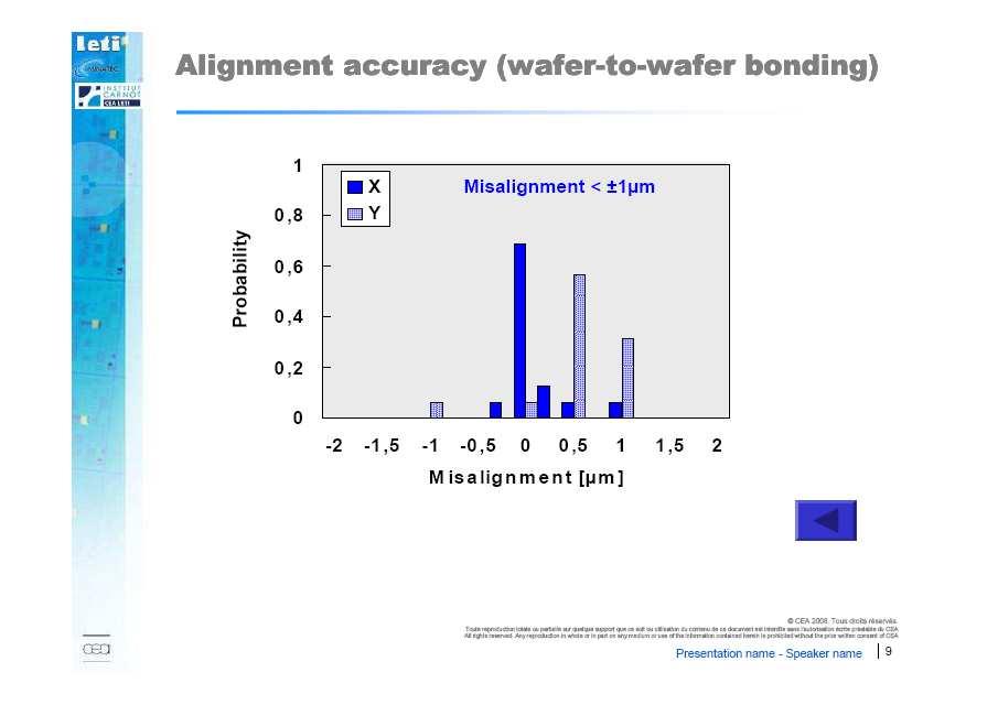
24 Step 6: Molecular wafer bonding Alignement of the two wafers (+-2µm) and bonding of photonic wafer on CMOS wafer CMOS wafer transistors metal interconnects 24
25 25
26 Step 7: Si Substrate removal Mechanical grinding Si chemical etching FC Modulator AWG Ge PD CMOS wafer transistors metal interconnects 26


27 SOI wafer bonded on a CMOS wafer Silicon rib waveguide Germanium 27
28 Step 8: InP heterostructure bonding Bond small InP dice with herostructure on the remaining BOX InP substrate removal of the dies FC Modulator AWG Ge PD CMOS wafer transistors metal interconnects 28
29 Step 9: InP heterostructure process Process InP source (InP etching) Planarized with SiO2 FC InP source Modulator AWG Ge PD CMOS wafer transistors metal interconnects 29
30 Step 10: Vias formation Lithos for different depths Etching SiO2 FC InP source Modulator AWG Ge PD CMOS wafer transistors metal interconnects 30
31 Step 11: Metal formation Metal deposition Metal etching PAD FC InP source Modulator AWG Ge PD CMOS wafer transistors metal interconnects 31
32 Summary Optimisation of 200mm InP on Si technology on-going Die to 200mm wafer molecular bonding DUV lithography on die InP etching Compatible metallisation LED and Laser demonstrated on Si Two ways to integrate InP on CMOS Above IC Back side with TSV Contamination issue is manageable 32
33 Acknowledgements All partners of HELIOS project THANK YOU FOR YOUR ATTENTION! 33
Lecture: Integration of silicon photonics with electronics. Prepared by Jean-Marc FEDELI CEA-LETI
 Lecture: Integration of silicon photonics with electronics Prepared by Jean-Marc FEDELI CEA-LETI Context The goal is to give optical functionalities to electronics integrated circuit (EIC) The objectives
IEEE JOURNAL OF SELECTED TOPICS IN QUANTUM ELECTRONICS 2010 Silicon Photonic Circuits: On-CMOS Integration, Fiber Optical Coupling, and Packaging
 IEEE JOURNAL OF SELECTED TOPICS IN QUANTUM ELECTRONICS 2010 Silicon Photonic Circuits: On-CMOS Integration, Fiber Optical Coupling, and Packaging Christophe Kopp, St ephane Bernab e, Badhise Ben Bakir,
VERSATILE SILICON PHOTONIC PLATFORM FOR DATACOM AND COMPUTERCOM APPLICATIONS. B Szelag CEA-Leti
 VERSATILE SILICON PHOTONIC PLATFORM FOR DATACOM AND COMPUTERCOM APPLICATIONS B Szelag CEA-Leti OUTLINE Silicon photonic : 200mm CMOS core technology towards 300mm Emergent needs vs core process Technological
NEXT GENERATION SILICON PHOTONICS FOR COMPUTING AND COMMUNICATION PHILIPPE ABSIL
 NEXT GENERATION SILICON PHOTONICS FOR COMPUTING AND COMMUNICATION PHILIPPE ABSIL OUTLINE Introduction Platform Overview Device Library Overview What s Next? Conclusion OUTLINE Introduction Platform Overview
Dries Van Thourhout IPRM 08, Paris
 III-V silicon heterogeneous integration ti Dries Van Thourhout IPRM 08, Paris InP/InGaAsP epitaxial layer stack Si WG DVS- BCB SiO 2 200nm III-V silicon heterogeneous integration ti Dries Van Thourhout
Heinrich-Hertz-Institut Berlin
 NOVEMBER 24-26, ECOLE POLYTECHNIQUE, PALAISEAU OPTICAL COUPLING OF SOI WAVEGUIDES AND III-V PHOTODETECTORS Ludwig Moerl Heinrich-Hertz-Institut Berlin Photonic Components Dept. Institute for Telecommunications,,
Index. Cambridge University Press Silicon Photonics Design Lukas Chrostowski and Michael Hochberg. Index.
 absorption, 69 active tuning, 234 alignment, 394 396 apodization, 164 applications, 7 automated optical probe station, 389 397 avalanche detector, 268 back reflection, 164 band structures, 30 bandwidth
Silicon Photonics Technology Platform To Advance The Development Of Optical Interconnects
 Silicon Photonics Technology Platform To Advance The Development Of Optical Interconnects By Mieke Van Bavel, science editor, imec, Belgium; Joris Van Campenhout, imec, Belgium; Wim Bogaerts, imec s associated
Silicon photonics with low loss and small polarization dependency. Timo Aalto VTT Technical Research Centre of Finland
 Silicon photonics with low loss and small polarization dependency Timo Aalto VTT Technical Research Centre of Finland EPIC workshop in Tokyo, 9 th November 2017 VTT Technical Research Center of Finland
Silicon photonics on 3 and 12 μm thick SOI for optical interconnects Timo Aalto VTT Technical Research Centre of Finland
 Silicon photonics on 3 and 12 μm thick SOI for optical interconnects Timo Aalto VTT Technical Research Centre of Finland 5th International Symposium for Optical Interconnect in Data Centres in ECOC, Gothenburg,
PROJECT FINAL REPORT
 PROJECT FINAL REPORT Grant Agreement number: FP7-224312 Project acronym: HELIOS Project title: photonics ELectronics functional Integration on CMOS Funding Scheme: Large Scale Integrating Project Period
Silicon Photonics Photo-Detector Announcement. Mario Paniccia Intel Fellow Director, Photonics Technology Lab
 Silicon Photonics Photo-Detector Announcement Mario Paniccia Intel Fellow Director, Photonics Technology Lab Agenda Intel s Silicon Photonics Research 40G Modulator Recap 40G Photodetector Announcement
64 Channel Flip-Chip Mounted Selectively Oxidized GaAs VCSEL Array
 64 Channel Flip-Chip Mounted Selectively Oxidized GaAs VCSEL Array 69 64 Channel Flip-Chip Mounted Selectively Oxidized GaAs VCSEL Array Roland Jäger and Christian Jung We have designed and fabricated
Silicon Photonics : Towards Heterogeneous and Multi-layer Integration for High Density Circuits
 Silicon Photonics : Towards Heterogeneous and Multi-layer Integration for High Density Circuits Stéphane Bernabé, Ségolène Olivier, Bertrand Szelag, Daivid Fowler, Christophe Kopp OPTICS, Dresden, 23-03-16
Opportunities and challenges of silicon photonics based System-In-Package
 Opportunities and challenges of silicon photonics based System-In-Package ECTC 2014 Panel session : Emerging Technologies and Market Trends of Silicon Photonics Speaker : Stéphane Bernabé (Leti Photonics
Convergence Challenges of Photonics with Electronics
 Convergence Challenges of Photonics with Electronics Edward Palen, Ph.D., P.E. PalenSolutions - Optoelectronic Packaging Consulting www.palensolutions.com palensolutions@earthlink.net 415-850-8166 October
Electronic-Photonic ICs for Low Cost and Scalable Datacenter Solutions
 Electronic-Photonic ICs for Low Cost and Scalable Datacenter Solutions Christoph Theiss, Director Packaging Christoph.Theiss@sicoya.com 1 SEMICON Europe 2016, October 27 2016 Sicoya Overview Spin-off from
New advances in silicon photonics Delphine Marris-Morini
 New advances in silicon photonics Delphine Marris-Morini P. Brindel Alcatel-Lucent Bell Lab, Nozay, France New Advances in silicon photonics D. Marris-Morini, L. Virot*, D. Perez-Galacho, X. Le Roux, D.
Fabrication of High-Speed Resonant Cavity Enhanced Schottky Photodiodes
 Fabrication of High-Speed Resonant Cavity Enhanced Schottky Photodiodes Abstract We report the fabrication and testing of a GaAs-based high-speed resonant cavity enhanced (RCE) Schottky photodiode. The
Integration of Optoelectronic and RF Devices for Applications in Optical Interconnect and Wireless Communication
 Integration of Optoelectronic and RF Devices for Applications in Optical Interconnect and Wireless Communication Zhaoran (Rena) Huang Assistant Professor Department of Electrical, Computer and System Engineering
Photonic Integrated Circuits Made in Berlin
 Fraunhofer Heinrich Hertz Institute Photonic Integrated Circuits Made in Berlin Photonic integration Workshop, Columbia University, NYC October 2015 Moritz Baier, Francisco M. Soares, Norbert Grote Fraunhofer
A 3.9 ns 8.9 mw 4 4 Silicon Photonic Switch Hybrid-Integrated with CMOS Driver
 A 3.9 ns 8.9 mw 4 4 Silicon Photonic Switch Hybrid-Integrated with CMOS Driver A. Rylyakov, C. Schow, B. Lee, W. Green, J. Van Campenhout, M. Yang, F. Doany, S. Assefa, C. Jahnes, J. Kash, Y. Vlasov IBM
OPTICAL I/O RESEARCH PROGRAM AT IMEC
 OPTICAL I/O RESEARCH PROGRAM AT IMEC IMEC CORE CMOS PHILIPPE ABSIL, PROGRAM DIRECTOR JORIS VAN CAMPENHOUT, PROGRAM MANAGER SCALING TRENDS IN CHIP-LEVEL I/O RECENT EXAMPLES OF HIGH-BANDWIDTH I/O Graphics
Si CMOS Technical Working Group
 Si CMOS Technical Working Group CTR, Spring 2008 meeting Markets Interconnects TWG Breakouts Reception TWG reports Si CMOS: photonic integration E-P synergy - Integration - Standardization - Cross-market
Innovative ultra-broadband ubiquitous Wireless communications through terahertz transceivers ibrow
 Project Overview Innovative ultra-broadband ubiquitous Wireless communications through terahertz transceivers ibrow Mar-2017 Presentation outline Project key facts Motivation Project objectives Project
Acknowledgements. Outline. Outline. III-V Silicon heterogeneous integration for integrated transmitters and receivers. Sources Detectors Bonding
 Acknowledgements III-V licon heterogeneous integration for integrated transmitters and receivers Dries Van Thourhout, J. Van Campenhout*, G. Roelkens, J. Brouckaert, R. Baets Ghent University / IMEC, Belgium
Envisioning the Future of Optoelectronic Interconnects:
 Envisioning the Future of Optoelectronic Interconnects: The Production Economics of InP and Si Platforms for 100G Ethernet LAN Transceivers Shan Liu Dr. Erica Fuchs Prof. Randolph Kirchain MIT Microphotonics
Silicon Photonics: A Platform for Integration, Wafer Level Assembly and Packaging
 Silicon Photonics: A Platform for Integration, Wafer Level Assembly and Packaging M. Asghari Kotura Inc April 27 Contents: Who is Kotura Choice of waveguide technology Challenges and merits of Si photonics
EPIC: The Convergence of Electronics & Photonics
 EPIC: The Convergence of Electronics & Photonics K-Y Tu, Y.K. Chen, D.M. Gill, M. Rasras, S.S. Patel, A.E. White ell Laboratories, Lucent Technologies M. Grove, D.C. Carothers, A.T. Pomerene, T. Conway
Research Article Development of Silicon Photonics Devices Using Microelectronic Tools for the Integration on Top of a CMOS Wafer
 Advances in Optical Technologies Volume 28, Article ID 412518, 15 pages doi:1.1155/28/412518 Research Article Development of licon Photonics Devices Using Microelectronic Tools for the Integration on Top
SUPPLEMENTARY INFORMATION
 Room-temperature continuous-wave electrically injected InGaN-based laser directly grown on Si Authors: Yi Sun 1,2, Kun Zhou 1, Qian Sun 1 *, Jianping Liu 1, Meixin Feng 1, Zengcheng Li 1, Yu Zhou 1, Liqun
Near/Mid-Infrared Heterogeneous Si Photonics
 PHOTONICS RESEARCH GROUP Near/Mid-Infrared Heterogeneous Si Photonics Zhechao Wang, PhD Photonics Research Group Ghent University / imec, Belgium ICSI-9, Montreal PHOTONICS RESEARCH GROUP 1 Outline Ge-on-Si
High-speed Ge photodetector monolithically integrated with large cross silicon-on-insulator waveguide
 [ APPLIED PHYSICS LETTERS ] High-speed Ge photodetector monolithically integrated with large cross silicon-on-insulator waveguide Dazeng Feng, Shirong Liao, Roshanak Shafiiha. etc Contents 1. Introduction
NOVEL CHIP GEOMETRIES FOR THz SCHOTTKY DIODES
 Page 404 NOVEL CHIP GEOMETRIES FOR THz SCHOTTKY DIODES W. M. Kelly, Farran Technology Ltd., Cork, Ireland S. Mackenzie and P. Maaskant, National Microelectronics Research Centre, University College, Cork,
AWG OPTICAL DEMULTIPLEXERS: FROM DESIGN TO CHIP. D. Seyringer
 AWG OPTICAL DEMULTIPLEXERS: FROM DESIGN TO CHIP D. Seyringer Research Centre for Microtechnology, Vorarlberg University of Applied Sciences, Hochschulstr. 1, 6850 Dornbirn, Austria, E-mail: dana.seyringer@fhv.at
CMP for More Than Moore
 2009 Levitronix Conference on CMP Gerfried Zwicker Fraunhofer Institute for Silicon Technology ISIT Itzehoe, Germany gerfried.zwicker@isit.fraunhofer.de Contents Moore s Law and More Than Moore Comparison:
Silicon Photonics Opportunity, applications & Recent Results
 Silicon Photonics Opportunity, applications & Recent Results Dr. Mario Paniccia Intel Fellow Director, Photonics Technology Lab Intel Corporation www.intel.com/go/sp Purdue University Oct 5 2007 Agenda
InP-based waveguide photodiodes heterogeneously integrated on silicon-oninsulator for photonic microwave generation
 InP-based waveguide photodiodes heterogeneously integrated on silicon-oninsulator for photonic microwave generation Andreas Beling, 1,* Allen S. Cross, 1 Molly Piels, 2 Jon Peters, 2 Qiugui Zhou, 1 John
CHAPTER 2 POLARIZATION SPLITTER- ROTATOR BASED ON A DOUBLE- ETCHED DIRECTIONAL COUPLER
 CHAPTER 2 POLARIZATION SPLITTER- ROTATOR BASED ON A DOUBLE- ETCHED DIRECTIONAL COUPLER As we discussed in chapter 1, silicon photonics has received much attention in the last decade. The main reason is
Fabricating 2.5D, 3D, 5.5D Devices
 Fabricating 2.5D, 3D, 5.5D Devices Bob Patti, CTO rpatti@tezzaron.com Tezzar on Semiconduct or 04/15/2013 1 Gen4 Dis-Integrated 3D Memory DRAM layers 42nm node 2 million vertical connections per lay per
Foundry processes for silicon photonics. Pieter Dumon 7 April 2010 ECIO
 Foundry processes for silicon photonics Pieter Dumon 7 April 2010 ECIO Photonics Research Group http://photonics.intec.ugent.be epixfab Prototyping Training Multi project wafer access to silicon photonic
Silicon Photonics: an Industrial Perspective
 Silicon Photonics: an Industrial Perspective Antonio Fincato Advanced Programs R&D, Cornaredo, Italy OUTLINE 2 Introduction Silicon Photonics Concept 300mm (12 ) Photonic Process Main Silicon Photonics
InP-based Waveguide Photodetector with Integrated Photon Multiplication
 InP-based Waveguide Photodetector with Integrated Photon Multiplication D.Pasquariello,J.Piprek,D.Lasaosa,andJ.E.Bowers Electrical and Computer Engineering Department University of California, Santa Barbara,
Silicon Photonics in Optical Communications. Lars Zimmermann, IHP, Frankfurt (Oder), Germany
, Germany") Silicon Photonics in Optical Communications Lars Zimmermann, IHP, Frankfurt (Oder), Germany Outline IHP who we are Silicon photonics Photonic-electronic integration IHP photonic technology Conclusions
Silicon Photonics in Optical Communications Lars Zimmermann, IHP, Frankfurt (Oder), Germany Outline IHP who we are Silicon photonics Photonic-electronic integration IHP photonic technology Conclusions
Silicon-Organic hybrid Fabrication platform for Integrated circuits FP7-ICT GA No
 www.sofi-ict.eu FP7-ICT-2009.3.8 GA No. 248609 Participants: 2 Outline Today s High Speed Interconnects Vision : Convergence of Photonics & Electronics Silicon Photonics Technology Silicon-Organic Hybrid
The Light at the End of the Wire. Dana Vantrease + HP Labs + Mikko Lipasti
 The Light at the End of the Wire Dana Vantrease + HP Labs + Mikko Lipasti 1 Goals of This Talk Why should we (architects) be interested in optics? How does on-chip optics work? What can we build with optics?
for optical communication system
 High speed Ge waveguide detector for optical communication system Xingjun Wang, Zhijuan Tu and Zhiping Zhou State Key Laboratory of Advanced Optical Communication Systems and Networks, School of Electronics
Integrated Photonics using the POET Optical InterposerTM Platform
 Integrated Photonics using the POET Optical InterposerTM Platform Dr. Suresh Venkatesan CIOE Conference Shenzhen, China Sept. 5, 2018 POET Technologies Inc. TSXV: PUBLIC POET PTK.V Technologies Inc. PUBLIC
Figure 1 Basic waveguide structure
 Recent Progress in SOI Nanophotonic Waveguides D. Van Thourhout, P. Dumon, W. Bogaerts, G. Roelkens, D. Taillaert, G. Priem, R. Baets IMEC-Ghent University, Department of Information Technology, St. Pietersnieuwstraat
Silicon-On-Insulator based guided wave optical clock distribution
 Silicon-On-Insulator based guided wave optical clock distribution K. E. Moselund, P. Dainesi, and A. M. Ionescu Electronics Laboratory Swiss Federal Institute of Technology People and funding EPFL Project
Jan Bogaerts imec
 imec 2007 1 Radiometric Performance Enhancement of APS 3 rd Microelectronic Presentation Days, Estec, March 7-8, 2007 Outline Introduction Backside illuminated APS detector Approach CMOS APS (readout)
FOUNDRY SERVICE. SEI's FEATURE. Wireless Devices FOUNDRY SERVICE. SRD-800DD, SRD-500DD D-FET Process Lg=0.8, 0.5µm. Ion Implanted MESFETs SRD-301ED
 FOUNDRY SERVICE 01.04. Foundry services have been one of the core businesses at SEI, providing sophisticated GaAs IC technology for all customers. SEI offers very flexible service to support the customers
High-efficiency, high-speed VCSELs with deep oxidation layers
 Manuscript for Review High-efficiency, high-speed VCSELs with deep oxidation layers Journal: Manuscript ID: Manuscript Type: Date Submitted by the Author: Complete List of Authors: Keywords: Electronics
CMOS Digital Integrated Circuits Lec 2 Fabrication of MOSFETs
 CMOS Digital Integrated Circuits Lec 2 Fabrication of MOSFETs 1 CMOS Digital Integrated Circuits 3 rd Edition Categories of Materials Materials can be categorized into three main groups regarding their
Hetero Silicon Photonics: Components, systems, packaging and beyond
 Silicon Photonics Hetero Silicon Photonics: Components, systems, packaging and beyond Thursday, October 9, 2014 Tolga Tekin and Rifat Kisacik Photonic & Plasmonic Systems, Fraunhofer for Reliability and
Progress Towards Computer-Aided Design For Complex Photonic Integrated Circuits
 Department of Electrical and Computer Engineering Progress Towards Computer-Aided Design For Complex Photonic Integrated Circuits Wei-Ping Huang Department of Electrical and Computer Engineering McMaster
A Fully Integrated 20 Gb/s Optoelectronic Transceiver Implemented in a Standard
 A Fully Integrated 20 Gb/s Optoelectronic Transceiver Implemented in a Standard 0.13 µm CMOS SOI Technology School of Electrical and Electronic Engineering Yonsei University 이슬아 1. Introduction 2. Architecture
Gallium nitride (GaN)
") 80 Technology focus: GaN power electronics Vertical, CMOS and dual-gate approaches to gallium nitride power electronics US research company HRL Laboratories has published a number of papers concerning
80 Technology focus: GaN power electronics Vertical, CMOS and dual-gate approaches to gallium nitride power electronics US research company HRL Laboratories has published a number of papers concerning
Introduction Fundamentals of laser Types of lasers Semiconductor lasers
 ECE 5368 Introduction Fundamentals of laser Types of lasers Semiconductor lasers Introduction Fundamentals of laser Types of lasers Semiconductor lasers How many types of lasers? Many many depending on
Ultra High-Speed InGaAs Nano-HEMTs
 Ultra High-Speed InGaAs Nano-HEMTs 2003. 10. 14 Kwang-Seok Seo School of Electrical Eng. and Computer Sci. Seoul National Univ., Korea Contents Introduction to InGaAsNano-HEMTs Nano Patterning Process
Examination Optoelectronic Communication Technology. April 11, Name: Student ID number: OCT1 1: OCT 2: OCT 3: OCT 4: Total: Grade:
 Examination Optoelectronic Communication Technology April, 26 Name: Student ID number: OCT : OCT 2: OCT 3: OCT 4: Total: Grade: Declaration of Consent I hereby agree to have my exam results published on
IWORID J. Schmitz page 1. Wafer-level CMOS post-processing Jurriaan Schmitz
 IWORID J. Schmitz page 1 Wafer-level CMOS post-processing Jurriaan Schmitz IWORID J. Schmitz page 2 Outline Introduction on wafer-level post-proc. CMOS: a smart, but fragile substrate Post-processing steps
SiGe BiCMOS and Photonic technologies for high frequency and communication applications Andreas Mai
 SiGe BiCMOS and Photonic technologies for high frequency and communication applications Andreas Mai Department Head Technology Outline Introduction & Motivation SiGe HBT device developments for high RF
An Example Design using the Analog Photonics Component Library. 3/21/2017 Benjamin Moss
 An Example Design using the Analog Photonics Component Library 3/21/2017 Benjamin Moss Component Library Elements Passive Library Elements: Component Current specs 1 Edge Couplers (Si)
EE 330 Lecture 7. Design Rules. IC Fabrication Technology Part 1
 EE 330 Lecture 7 Design Rules IC Fabrication Technology Part 1 Review from Last Time Technology Files Provide Information About Process Process Flow (Fabrication Technology) Model Parameters Design Rules
High Speed pin Photodetector with Ultra-Wide Spectral Responses
 High Speed pin Photodetector with Ultra-Wide Spectral Responses C. Tam, C-J Chiang, M. Cao, M. Chen, M. Wong, A. Vazquez, J. Poon, K. Aihara, A. Chen, J. Frei, C. D. Johns, Ibrahim Kimukin, Achyut K. Dutta
High-Speed Scalable Silicon-MoS 2 P-N Heterojunction Photodetectors
 High-Speed Scalable Silicon-MoS 2 P-N Heterojunction Photodetectors Veerendra Dhyani 1, and Samaresh Das 1* 1 Centre for Applied Research in Electronics, Indian Institute of Technology Delhi, New Delhi-110016,
High Power RF MEMS Switch Technology
 High Power RF MEMS Switch Technology Invited Talk at 2005 SBMO/IEEE MTT-S International Conference on Microwave and Optoelectronics Conference Dr Jia-Sheng Hong Heriot-Watt University Edinburgh U.K. 1
Alternatives to standard MOSFETs. What problems are we really trying to solve?
 Alternatives to standard MOSFETs A number of alternative FET schemes have been proposed, with an eye toward scaling up to the 10 nm node. Modifications to the standard MOSFET include: Silicon-in-insulator
SAMPLE SLIDES & COURSE OUTLINE. Core Competency In Semiconductor Technology: 2. FABRICATION. Dr. Theodore (Ted) Dellin
 Dellin") & Digging Deeper Devices, Fabrication & Reliability For More Info:.com or email Dellin@ieee.org SAMPLE SLIDES & COURSE OUTLINE In : 2. A Easy, Effective, of How Devices Are.. Recommended for everyone who
& Digging Deeper Devices, Fabrication & Reliability For More Info:.com or email Dellin@ieee.org SAMPLE SLIDES & COURSE OUTLINE In : 2. A Easy, Effective, of How Devices Are.. Recommended for everyone who
InP-based Waveguide Photodetector with Integrated Photon Multiplication
 InP-based Waveguide Photodetector with Integrated Photon Multiplication D.Pasquariello,J.Piprek,D.Lasaosa,andJ.E.Bowers Electrical and Computer Engineering Department University of California, Santa Barbara,
Fabrication and Characterization of Broad-Area Lasers with Dry-Etched Mirrors
 Broad-Area Lasers with Dry-Etched Mirrors 31 Fabrication and Characterization of Broad-Area Lasers with Dry-Etched Mirrors Franz Eberhard and Eckard Deichsel Using reactive ion-beam etching (RIBE) we have
Hybrid vertical-cavity laser integration on silicon
 Invited Paper Hybrid vertical-cavity laser integration on Emanuel P. Haglund* a, Sulakshna Kumari b,c, Johan S. Gustavsson a, Erik Haglund a, Gunther Roelkens b,c, Roel G. Baets b,c, and Anders Larsson
Miniature Mid-Infrared Thermooptic Switch with Photonic Crystal Waveguide Based Silicon-on-Sapphire Mach Zehnder Interferometers
 Miniature Mid-Infrared Thermooptic Switch with Photonic Crystal Waveguide Based Silicon-on- Mach Zehnder Interferometers Yi Zou, 1,* Swapnajit Chakravarty, 2,* Chi-Jui Chung, 1 1, 2, * and Ray T. Chen
May 21-23, 2012 Białystok, Poland
 6 th International Forum May 21-23, 2012 Białystok, Poland Photonic integrated circuits and generic integration concept. Photonic solutions for research institutes, SME's and large companies Katarzyna
Low Thermal Resistance Flip-Chip Bonding of 850nm 2-D VCSEL Arrays Capable of 10 Gbit/s/ch Operation
 Low Thermal Resistance Flip-Chip Bonding of 85nm -D VCSEL Arrays Capable of 1 Gbit/s/ch Operation Hendrik Roscher In 3, our well established technology of flip-chip mounted -D 85 nm backside-emitting VCSEL
PROJECT. DOCUMENT IDENTIFICATION D2.2 - Report on low cost filter deposition process DISSEMINATION STATUS PUBLIC DUE DATE 30/09/2011 ISSUE 2 PAGES 16
 GRANT AGREEMENT NO. ACRONYM TITLE CALL FUNDING SCHEME 248898 PROJECT 2WIDE_SENSE WIDE spectral band & WIDE dynamics multifunctional imaging SENSor ENABLING SAFER CAR TRANSPORTATION FP7-ICT-2009.6.1 STREP
InP-based Photonic Integration: Learning from CMOS
 InP-based Photonic Integration: Learning from CMOS Meint Smit Roel Baets Mike Wale COBRA TU Eindhoven IMEC U Gent Oclaro Receive Transmit Transponder-based DWDM FOE 2009, LS InP PIC in Dig Comm Networks,
End-of-line Standard Substrates For the Characterization of organic
 FRAUNHOFER INSTITUTe FoR Photonic Microsystems IPMS End-of-line Standard Substrates For the Characterization of organic semiconductor Materials Over the last few years, organic electronics have become
Heterogeneous Integration of Silicon and AlGaInAs for a Silicon Evanescent Laser
 Invited Paper Heterogeneous Integration of Silicon and AlGaInAs for a Silicon Evanescent Laser Alexander W. Fang a, Hyundai Park a, Richard Jones b, Oded Cohen c, Mario J. Paniccia b, and John E. Bowers
Flip-Chip Integration of 2-D 850 nm Backside Emitting Vertical Cavity Laser Diode Arrays
 Flip-Chip Integration of 2-D 850 nm Backside Emitting Vertical Cavity Laser Diode Arrays Hendrik Roscher Two-dimensional (2-D) arrays of 850 nm substrate side emitting oxide-confined verticalcavity lasers
High Speed Detectors. Andreas Umbach ECOC 2009, Workshop 7 Monolithic and Hybrid Photonic Integrated Transceivers for Advanced Modulation Formats
 High Speed Detectors Andreas Umbach ECOC 2009, Workshop 7 Monolithic and Hybrid Photonic Integrated Transceivers for Advanced Modulation Formats 100 Gbit/s Long-Haul Transport Optical networks use "standardized"
Winter College on Optics: Fundamentals of Photonics - Theory, Devices and Applications February 2014
 2572-10 Winter College on Optics: Fundamentals of Photonics - Theory, Devices and Applications 10-21 February 2014 Photonic packaging and integration technologies II Sonia M. García Blanco University of
An electrically pumped germanium laser
 An electrically pumped germanium laser The MIT Faculty has made this article openly available. Please share how this access benefits you. Your story matters. Citation As Published Publisher Camacho-Aguilera,
Propagation loss study of very compact GaAs/AlGaAs substrate removed waveguides
 Propagation loss study of very compact GaAs/AlGaAs substrate removed waveguides JaeHyuk Shin, Yu-Chia Chang and Nadir Dagli * Electrical and Computer Engineering Department, University of California at
Integrated diodes. The forward voltage drop only slightly depends on the forward current. ELEKTRONIKOS ĮTAISAI
 1 Integrated diodes pn junctions of transistor structures can be used as integrated diodes. The choice of the junction is limited by the considerations of switching speed and breakdown voltage. The forward
High speed silicon-based optoelectronic devices Delphine Marris-Morini Institut d Electronique Fondamentale, Université Paris Sud
 High speed silicon-based optoelectronic devices Delphine Marris-Morini Institut d Electronique Fondamentale, Université Paris Sud Data centers Optical telecommunications Environment Interconnects Silicon
Grating coupled photonic crystal demultiplexer with integrated detectors on InPmembrane
 Grating coupled photonic crystal demultiplexer with integrated detectors on InPmembrane F. Van Laere, D. Van Thourhout and R. Baets Department of Information Technology-INTEC Ghent University-IMEC Ghent,
Silicon Photonics Transceivers for Hyper Scale Datacenters: Deployment and Roadmap
 Silicon Photonics Transceivers for Hyper Scale Datacenters: Deployment and Roadmap Peter De Dobbelaere Luxtera Inc. 09/19/2016 Luxtera Proprietary www.luxtera.com Luxtera Company Introduction $100B+ Shift
Si Photonics Technology Platform for High Speed Optical Interconnect. Peter De Dobbelaere 9/17/2012
 Si Photonics Technology Platform for High Speed Optical Interconnect Peter De Dobbelaere 9/17/2012 ECOC 2012 - Luxtera Proprietary www.luxtera.com Overview Luxtera: Introduction Silicon Photonics: Introduction
Feature-level Compensation & Control
 Feature-level Compensation & Control 2 Sensors and Control Nathan Cheung, Kameshwar Poolla, Costas Spanos Workshop 11/19/2003 3 Metrology, Control, and Integration Nathan Cheung, UCB SOI Wafers Multi wavelength
Project Overview. Innovative ultra-broadband ubiquitous Wireless communications through terahertz transceivers ibrow
 Project Overview Innovative ultra-broadband ubiquitous Wireless communications through terahertz transceivers ibrow Presentation outline Key facts Consortium Motivation Project objective Project description
Simulation of High Resistivity (CMOS) Pixels
 Pixels") Simulation of High Resistivity (CMOS) Pixels Stefan Lauxtermann, Kadri Vural Sensor Creations Inc. AIDA-2020 CMOS Simulation Workshop May 13 th 2016 OUTLINE 1. Definition of High Resistivity Pixel Also
Simulation of High Resistivity (CMOS) Pixels Stefan Lauxtermann, Kadri Vural Sensor Creations Inc. AIDA-2020 CMOS Simulation Workshop May 13 th 2016 OUTLINE 1. Definition of High Resistivity Pixel Also
Optical Fiber Communication Lecture 11 Detectors
 Optical Fiber Communication Lecture 11 Detectors Warriors of the Net Detector Technologies MSM (Metal Semiconductor Metal) PIN Layer Structure Semiinsulating GaAs Contact InGaAsP p 5x10 18 Absorption InGaAs
Monolithically integrated InGaAs nanowires on 3D. structured silicon-on-insulator as a new platform for. full optical links
 Monolithically integrated InGaAs nanowires on 3D structured silicon-on-insulator as a new platform for full optical links Hyunseok Kim 1, Alan C. Farrell 1, Pradeep Senanayake 1, Wook-Jae Lee 1,* & Diana.
Ultralinear heterogeneously integrated ring-assisted Mach Zehnder interferometer modulator on silicon
 Research Article Vol. 3, No. 12 / December 2016 / Optica 1483 Ultralinear heterogeneously integrated ring-assisted Mach Zehnder interferometer modulator on silicon CHONG ZHANG, 1, *PAUL A. MORTON, 2 JACOB
Silicon photonics integration roadmap for applications in computing systems
 Silicon photonics integration roadmap for applications in computing systems Bert Jan Offrein Neuromorphic Devices and Systems Group 2016 IBM Corporation Outline Photonics and computing? The interconnect
Lecture 7. Lithography and Pattern Transfer. Reading: Chapter 7
 Lecture 7 Lithography and Pattern Transfer Reading: Chapter 7 Used for Pattern transfer into oxides, metals, semiconductors. 3 types of Photoresists (PR): Lithography and Photoresists 1.) Positive: PR
Silicon Photonics Opportunity, Applicatoins & Recent Results. Mario Paniccia, Director Photonics Technology Lab Intel Corporation
 Silicon Photonics Opportunity, Applicatoins & Recent Results Mario Paniccia, Director Photonics Technology Lab Intel Corporation Intel Corporation CREOL April 1 2005 Agenda Opportunity for Silicon Photonics
Supporting Information for Gbps terahertz external. modulator based on a composite metamaterial with a. double-channel heterostructure
 Supporting Information for Gbps terahertz external modulator based on a composite metamaterial with a double-channel heterostructure Yaxin Zhang, Shen Qiao*, Shixiong Liang, Zhenhua Wu, Ziqiang Yang*,