Dries Van Thourhout IPRM 08, Paris
|
|
|
- Letitia Owen
- 5 years ago
- Views:
Transcription


1 III-V silicon heterogeneous integration ti Dries Van Thourhout IPRM 08, Paris InP/InGaAsP epitaxial layer stack Si WG DVS- BCB SiO 2 200nm
2 III-V silicon heterogeneous integration ti Dries Van Thourhout IPRM 08, Paris InP/InGaAsP epitaxial layer stack Si WG DVS- BCB SiO 2 200nm 1. Silicon photonics is great!!! 2. But we still need InP 3. III-V silicon integration 4. Devices
3 Acknowledgements Photonics Research Group III-V silicon integration: G. Roelkens, J. Van Campenhout, J. Brouckaert, L. Liu Silicon Processing W. Bogaerts, P. Dumon, S. Selvarajan, R. Baets EU IST-PICMOS team J.M. Fedeli, L. Di Cioccio (LETI) (molecular bonding, processing) C. Seassal, P. Rojo-Romeo, P. Regreny, P. Viktorovitch (INL) (processing, epitaxy) R. Notzel, X.J.M. Leijtens (TU/e) (epitaxy) C. Lagahe, B. Aspar (TRACIT) (planarization)
4 III-V silicon heterogeneous integration ti InP/InGaAsP epitaxial layer stack Si WG DVS- BCB SiO 2 200nm 1. Silicon photonics is great!!! 2. But we still need InP 3. III-V silicon integration 4. Devices
 the solution to all")

 High refractive index")
 ) Compatible with")

5 Silicon photonics Width (500nm) x Height (220nm) the solution to all our problems? Transparent at telecom wavelengths (1.3 µm, 1.55 µm) High refractive index contrast ultra-compact circuits SiO 2 (1-2 µm) ) Compatible with CMOS-processing Highest Silicon quality processes High yield, high repeatability Integration with electronics Pattern definition: DUV litho`?

![Excess bend loss [db/90 0 ] 0.08 0.](/docs-images/87/97055451/images/6-1.jpg "06 0.04 0.02 0 0.09dB/90 0.")

6 Photonic wiring Low loss bends <0.3dB excess loss for splitters Excess bend loss [db/90 0 ] dB/ dB/ dB/ dB/ Radius [um] 97% transmission in crossings (b)


![mission [db]](/docs-images/87/97055451/images/7-2.jpg "-10-15 -20 1 2")


7 Wavelength dependent devices 0 FSR -5 transm mission [db] wavelength [nm]


8 Increasing Index Contrast Glass based devices Bend Radius ~ 5 mm 5 mm 5 cm 200 µm Silicon photonic ICs Bend Radius < 5µm InP/InGaAsP (bend radius ~ 500um)


9 Silicon Photonics Intel 40GHz Detector Fiber cable plugs here Luxtera Ethernet Tranceiver Ceramic Package IBM Modulator


10 Silicon Photonics Silicon photonics comes in many flavors Large rib type waveguides Small core devices Optimized for nanophotonics Small device size Easy coupling with fiber This work and many others Large device size e.g. Full CMOS integration Fabricated in CMOS process Directly integrated with electronics e.g.
11 III-V on silicon? Silicon photonics gives us: Excellent passives Fast modulators, fast photodetectors t t But: (almost) no light Need for integration ti with III-Vs Requirements High density (~10-20um device pitch) High alignment accuracy (~100nm) Waferscale processes
12 III-V silicon heterogeneous integration ti InP/InGaAsP epitaxial layer stack Si WG DVS- BCB SiO 2 200nm 1. Silicon photonics is great!!! 2. But we still need InP 3. III-V silicon integration 4. Devices
 low density of integration Hetero-epitaxial growth of III-V on silicon")

13 III-V on silicon There are several ways to integrate III-V VonSOI Flip-chip integration of opto-electronic components most rugged technology testing of opto-electronic components in advance slow sequential process (alignment accuracy) low density of integration Hetero-epitaxial growth of III-V on silicon collective process, high density of integration See other talks at this conference mismatch in lattice constant, CTE, polar/non-polar contamination and temperature budget Bonding of III-V epitaxial layers sequential but fast integration process high density of integration, collective processing high quality epitaxial III-V layers
14 Proposed integration process Starting point: Processed SOI-waveguide wafer 193nm or 248nm DUV lithography Fabricated in pilot CMOS-line


15 Proposed integration process Planarization Planarization Using BCB (50nm to 2um) (UGent/IMEC) Using SiO 2 (TRACIT - CEA-LETI)
16 Proposed integration process Die-to-wafer bonding Bonding InP-dies on top of planarized SOI-wafer Low alignment accuracy required Fast pick-and-place place


17 Proposed integration process Substrate removal Remove InP-substrate down to etch stop layer Remove etch stop Thin membrane remains (200nm ~ 2 µm)


18 Proposed integration process Hardmask deposition Micro-disk sources Detectors DBR sources Decontamination ti and hardmask deposition Alignment of waveguides and devices through lithographic methods
19 Proposed integration process Processing of InP-optoelectronic devices Mesa etching and Metallization Waferscale processing!!! on 2cm 2 pieces (UGent, INL) on 200mm wafers (CEA-LETI)
20 III-V/Silicon photonics Bonding of III-V epitaxial i layers Molecular die-to-wafer bonding Based on van der Waals attraction act between ee wafer surfaces Requires atomic contact between both surfaces - very sensitive to particles - very sensitive to roughness Adhesive die-to-wafer bonding - very sensitive to contamination of surfaces Uses an adhesive layer as a glue to stick both surfaces Requirements are more relaxed compared to Molecular - glue compensates for particles (some) - glue compensates for roughness (all) - glue allows (some) contamination of surfaces
21 Bonding Technology Requirements for the adhesive for bonding Optically transparent <0.1dB/cm High thermal stability (post-bonding thermal budget) 400C Low curing temperature (low thermal stress) No outgassing upon curing (void formation) Resistant to all kinds of chemicals 250C OK HCl,H 2 SO 4,H 2 O 2, DVS-BCB satisfies these requirements CH 3 CH 3 Si O Si CH 3 CH 3 1,3-divinyl-1,1,3,3-tetramethyldisiloxane-bisbenzocyclobutene


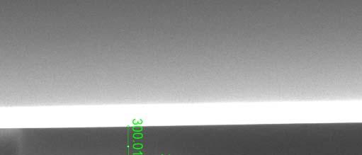
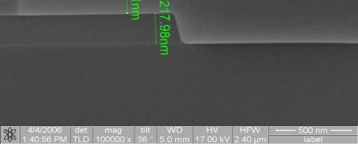
22 Bonding Technology Cross-sectional image of III-V/Silicon substrate InP/InGaAsP epitaxial layer stack InP-InGaAsP epitaxial layer stack DVS-BCB Si Si WG SiO 2 DVS-BCB 200nm Si SiO 2 200nm 300nm bonding layer routinely and reliably obtained


23 Bonding Technology Cross-sectional image of III-V/Silicon substrate InP/InGaAsP epitaxial layer stack InP-InGaAsP epitaxial layer stack DVS-BCB Si Si WG SiO 2 DVS-BCB 200nm Si SiO 2 200nm 300nm bonding layer routinely and reliably obtained Recently also sub-100nm layers demonstrated
24 III-V silicon heterogeneous integration ti InP/InGaAsP epitaxial layer stack Si WG DVS- BCB SiO 2 200nm 1. Silicon photonics is great!!! 2. But we still need InP 3. III-V silicon integration 4. Devices


25 Integrated Devices: laser diode Integrated t laser diodes d First only pulsed operation due to high thermal resistivity DVS-BCB Integration of a heat sink to improve heat dissipation Continuous wave operation achieved this way

 5 4 3 2 1 10 C 15 C 20 C 25 C 30")
 (IPRM 08, paper")
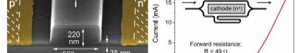
26 Other groups Intel / UCSB Hybrid laser CEA-LETI / III-V Vlab p-type contact 5 µm n-type contact III-V etched facet Output t power (mw) C 15 C 20 C 25 C 30 C 35 C 40 C Voltage (V V) Current (ma) (IPRM 08, paper MoA4.2) 0

 L=30µm, d=400nm no absorption 40µm contact window Ti/Au contact IN InGaAs")
27 MSM detectors Etching of detectors in III-V Spinning insulation layer of polyimide Opening contact window Metallization 25µm long detector InGaAs/ InAlAs polyimide R = 1.0A/W (1550nm), IQE = 80% (5V bias) I dark = 3nA (5V bias) contact window SOI waveguides (30µm pitch) L=30µm, d=400nm no absorption 40µm contact window Ti/Au contact IN InGaAs absorption 40µm IN
")


28 Wavelength selective filter V_bias = -10V 1 ) 1x4 demux, λ=20nm, 280µm x 150µm Photo o current (ma

29 Integrated microdisk laser Microdisk laser design Whispering-gallery modes Central top contact Bottom contact on thin lateral contact layer (t s ) Hole injection through a reverse-biased tunnel-junction bottom contact Si waveguide w Si d ox 2R disk top contact tunnel junction SiO 2 Si substrate active layer InP t s t Microdisk thickness 0.5 < t < 1µm Evanescent coupling to SOI wire waveguide (500x220nm 2 )
30 On-chip optical interconnect? Integrate t photonic interconnect t on CMOS? III-V material microlaser SOI waveguide microdetector SOI Optical Interconnect layer Electrical Interconnect layer Silicon transistor layer Need integrated interconnect layer on top of CMOS Silicon wiring for interconnect III-V microdevices for sources and detectors


31 PICMOS 25 µm A collaborative project InP island SOI waveguide microdisk IMEC: metallization III-V processing TU/e: detector etching IMEC: SOI-wafer fabrication INL: substrate removal INL: source etching SiO 2 BCB InP - InGaAsP TRACIT: planarization Si wire LETI: bonding LETI: hard mask 130-nm bonding layer Si substrate Six cleanrooms but still working devices
 Spectral pow wer (dbm) -20-30 -40-50 -60-70 -80 09 0.9mA 0 0 0.5 1 1.5 2 Current (ma) 0-90 1560 1580 1600 1620 1640 Wavelength (nm) Threshold current I th = 0.")

32 Output pow wer (µw) Continuous-wave lasing 1-µm thick, µm devices exhibit continuous-wave lasing CW power Pulsed peak power CW Voltage Voltage (V) Spectral pow wer (dbm) mA Current (ma) Wavelength (nm) Threshold current I th = 0.5mA, voltage V th = V BCB slope efficiency = 30µW/mA, up to 10µW InP - InGaAsP (Pulsed regime: up to 100µW peak power) SiO 2 Si wire J. Van Campenhout et al., "Electrically pumped inp-based microdisk lasers Si integrated substrate with a nanophotonic silicon-on-insulator waveguide circuit" Optics intec 2007 Express, nm Photonics May Research 2007 Group - b di
33 Temperature dependence Laser emission up to 70 C (pulsed operation) pow wer [a.u.] D = 6µm T=10 C T=20 C T=30 C T=40 C T=50 C peak wave elength [nm] T=60 C current [ua] T=70 C dλ 86 pmk dt Tamb [ C] dn ( InP) 210 dt dn dt ( BCB) K 3 1 K
34 Fit to experimental data 30 3 Optic cal Power (µw) pulsed data CW data ) Voltage (V Current (ma) Model can be fitted to pulsed experimental data, assuming: uniform injection: injection efficiency =0.36x0.7=0.25 coupling loss = 3cm -1 (simulation) tunnel-junction p-doping N a = 2x10 18 cm -3 (design target N a = 2x10 19 cm -3, SIMS analysis: N a ~ 8x10 18 cm -3 ) fitted scatter loss = 8cm -1 (passive ring resonators: 7-13cm -1 ) Consistent fit, except for tunnel-junction p-doping and saturation effect
 -10-20 -30-40 -50-60 dominant lasing wavelength of MDL w/o injection with injection λ FSR =32nm injected laser wavelength -70 1.56 1.")
35 Ultra-low-power Wavelength conversion tunable laser oscilloscope detector pattern generator polarization controller high-speed detector modulator band-pass filter variable attentuator EDFA polarization controller SOI wg. MDL mod de intensity (db Bm/0.1nm) dominant lasing wavelength of MDL w/o injection with injection λ FSR =32nm injected laser wavelength wavelength (µm) power (a.u.) ns time (ns) No control power needed. Wavelength conversion with only 6.4uW control power. 5Gbps dynamic results.
36 Full Link D Demonstrator t t di die (contains ( t i 256 optical ti l links) li k ) 7mm 264 Micro detectors (TU Ei Eindhoven dh / Cobra) C b ) FIBRE G GRATING C COUPLERS S Point-to--point links s 120 DBR microlasers Broadc cast links s Point-to--point links s FIBRE G GRATING C COUPLERS S 120 Microdisk lasers laser III-V die detector III-V die 9mm 200mm SOI wafer


37 Pulsed operation of the link monitor grating Duty cycle = 8% Period = 1 µs on-chip detector Detector not biased (0V), negligible gbedark current Performance under pulsed operation: Threshold current < 700 µa & Slope efficiency ~ 1.1 µw/ma Detector t efficiency i of f023029a/w A/W.
38 Outlook & conclusion We demonstrated: t d Ultra-dense waveguiding < 2 µm pitch (waveguide-to-waveguide) waveguide) A powerfull III-V on Silicon integration technology Several proof-of-principle of principle demonstrators Electrically pumped micro-disk sources on silicon platform 500 µa threshold current Micro-detectors on silicon platform 1.0A/W Fabrication using waferscale processes
39 Single wavelength Outlook & conclusion We still need to: Multi-wavelength sources Improve source performance Towards 50 µa threshold current 10GHz modulation speed 30% internal efficiency λ Through improved processing λ λ Through improved device design λ Improved high temperature operation Full fabrication in CMOS pilot-line 1 2line λ 1 λ 2 λ 3 N λ λ λ λ λ Integration with CMOS electronic driving circuit Implement WDM-functionality 3 N N λ 1,λ 2... λ N-1,λ N λ 1,λ 2... λ N-1,λ N
 D1 D4 D3 D2 D1 powe er (db) -20-30 -40-50 λ = 32nm FSR biased at: 3mA D2 D1 D4 D3 D2 D1-60 -60-70 1.56 1.57 1.58 1.59 1.6 1.61 1.62 wavelength (µm)")
40 Multi-wavelength Laser 4-wavelength laser D1 D2 D3 D4 SM fiber grating coupler powe er (db) (a) λ = 23nm FSR biased at: 4mA D2 10µm diameter 7.5µm diameter -10 (b) D1 D4 D3 D2 D1 powe er (db) λ = 32nm FSR biased at: 3mA D2 D1 D4 D3 D2 D wavelength (µm) wavelength (µm)
41 Outlook & conclusion We still need to: Improve source performance Towards 50 µa threshold current 10GHz modulation speed 30% internal efficiency Through improved processing Through improved device design Improved high temperature operation Full fabrication in CMOS pilot-line line Integration with CMOS electronic driving circuit Implement WDM-functionality Simplify overall processing

42 Outlook & conclusion Simplify processing Avoid critical patterning in the III-V layer Silicon racetrack III-V film
43 Acknowledgements Photonics Research Group III-V silicon integration: G. Roelkens, J. Van Campenhout, J. Brouckaert, L. Liu Silicon Processing W. Bogaerts, P. Dumon, S. Selvarajan, R. Baets PICMOS team J.M. Fedeli, L. Di Cioccio (LETI) (molecular bonding, processing) C. Lagahe, B. Aspar (TRACIT) (planarization) C. Seassal, P. Rojo-Romeo, P. Regreny, P. Viktorovitch (INL) (processing, epitaxy) R. Notzel, X.J.M. Leijtens (TU/e) (epitaxy)
44
45 Fiber-chip coupling Important: 1µm Low loss coupling Large bandwidth Coupling tolerance Fabrication Limited extra processing Tolerant to fabrication SOI wire Low reflection Polarization? Single-mode fiber


46 Coupling to fiber Grating coupler Alternative: Grating couplers Waferscale testing Waferscale packaging High alignment tolerance From Fibre Single mode fiber core shallow fibre coupler 70% efficiency measured deep trench Towards optical circuit


47 Increase effieciency? Top view Improving performance Add bottom mirror grating coupler Apodize Other With mirror Without mirror BCB FIB cross-section 1dB bandwidth > 40nm
48 Main Challenges 1. Coupling of light between III-V and Silicon Option 1: evanescent Guiding in silicon Requires thin bonding layer Requires III-V thinner than <250nm Option 2: other (adiabatic, grating coupler ) Guiding in III-V Thicker III-V layer Sometimes thicker bonding
49 Main Challenges 1. Coupling of light between III-V and Silicon Option 1: evanescent Guiding in silicon Requires thin bonding layer Requires III-V thinner than <250nm Loss at metal contact Option 2: other (adiabatic, grating coupler ) Guiding in III-V Thicker III-V layer Sometimes thicker bonding 2. Electrical injection Metal contact on membrane devices without inducing additional loss 3. Thermal management Overcome thermal barrier of bonding layer and BOX


50 Integrated Devices: laser diode Integrated laser diodes Fabry-Perot laser cavity by etching InP/InGaAsP laser facets Inverted adiabatic taper coupling approach
Acknowledgements. Outline. Outline. III-V Silicon heterogeneous integration for integrated transmitters and receivers. Sources Detectors Bonding
 Acknowledgements III-V licon heterogeneous integration for integrated transmitters and receivers Dries Van Thourhout, J. Van Campenhout*, G. Roelkens, J. Brouckaert, R. Baets Ghent University / IMEC, Belgium
Si and InP Integration in the HELIOS project
 Si and InP Integration in the HELIOS project J.M. Fedeli CEA-LETI, Grenoble ( France) ECOC 2009 1 Basic information about HELIOS HELIOS photonics ELectronics functional Integration on CMOS www.helios-project.eu
Lecture: Integration of silicon photonics with electronics. Prepared by Jean-Marc FEDELI CEA-LETI
 Lecture: Integration of silicon photonics with electronics Prepared by Jean-Marc FEDELI CEA-LETI Context The goal is to give optical functionalities to electronics integrated circuit (EIC) The objectives
Heterogenous integration of InP/InGaAsP photodetectors onto ultracompact Silicon-on-Insulator waveguide circuits
 Heterogenous integration of InP/InGaAsP photodetectors onto ultracompact Silicon-on-Insulator waveguide circuits Günther Roelkens, Joost Brouckaert, Dirk Taillaert, Pieter Dumon, Wim Bogaerts, Richard
A silicon nanophotonic platform for optical interconnects
 A silicon nanophotonic platform for optical interconnects D. Van Thourhout Photonics Research Group, Ghent University/ IMEC Dec. 9, 2010 Nanophotonic Devices for Optical Networks-On-Chip multi-l microdisk
Photonic Integrated Circuits Made in Berlin
 Fraunhofer Heinrich Hertz Institute Photonic Integrated Circuits Made in Berlin Photonic integration Workshop, Columbia University, NYC October 2015 Moritz Baier, Francisco M. Soares, Norbert Grote Fraunhofer
Heinrich-Hertz-Institut Berlin
 NOVEMBER 24-26, ECOLE POLYTECHNIQUE, PALAISEAU OPTICAL COUPLING OF SOI WAVEGUIDES AND III-V PHOTODETECTORS Ludwig Moerl Heinrich-Hertz-Institut Berlin Photonic Components Dept. Institute for Telecommunications,,
Grating coupled photonic crystal demultiplexer with integrated detectors on InPmembrane
 Grating coupled photonic crystal demultiplexer with integrated detectors on InPmembrane F. Van Laere, D. Van Thourhout and R. Baets Department of Information Technology-INTEC Ghent University-IMEC Ghent,
Integrated photonic circuit in silicon on insulator for Fourier domain optical coherence tomography
 Integrated photonic circuit in silicon on insulator for Fourier domain optical coherence tomography Günay Yurtsever *,a, Pieter Dumon a, Wim Bogaerts a, Roel Baets a a Ghent University IMEC, Photonics
Figure 1 Basic waveguide structure
 Recent Progress in SOI Nanophotonic Waveguides D. Van Thourhout, P. Dumon, W. Bogaerts, G. Roelkens, D. Taillaert, G. Priem, R. Baets IMEC-Ghent University, Department of Information Technology, St. Pietersnieuwstraat
Index. Cambridge University Press Silicon Photonics Design Lukas Chrostowski and Michael Hochberg. Index.
 absorption, 69 active tuning, 234 alignment, 394 396 apodization, 164 applications, 7 automated optical probe station, 389 397 avalanche detector, 268 back reflection, 164 band structures, 30 bandwidth
Silicon Photonics Technology Platform To Advance The Development Of Optical Interconnects
 Silicon Photonics Technology Platform To Advance The Development Of Optical Interconnects By Mieke Van Bavel, science editor, imec, Belgium; Joris Van Campenhout, imec, Belgium; Wim Bogaerts, imec s associated
Silicon Photonics: A Platform for Integration, Wafer Level Assembly and Packaging
 Silicon Photonics: A Platform for Integration, Wafer Level Assembly and Packaging M. Asghari Kotura Inc April 27 Contents: Who is Kotura Choice of waveguide technology Challenges and merits of Si photonics
A thin foil optical strain gage based on silicon-on-insulator microresonators
 A thin foil optical strain gage based on silicon-on-insulator microresonators D. Taillaert* a, W. Van Paepegem b, J. Vlekken c, R. Baets a a Photonics research group, Ghent University - INTEC, St-Pietersnieuwstraat
A continuous-wave Raman silicon laser
 A continuous-wave Raman silicon laser Haisheng Rong, Richard Jones,.. - Intel Corporation Ultrafast Terahertz nanoelectronics Lab Jae-seok Kim 1 Contents 1. Abstract 2. Background I. Raman scattering II.
NEXT GENERATION SILICON PHOTONICS FOR COMPUTING AND COMMUNICATION PHILIPPE ABSIL
 NEXT GENERATION SILICON PHOTONICS FOR COMPUTING AND COMMUNICATION PHILIPPE ABSIL OUTLINE Introduction Platform Overview Device Library Overview What s Next? Conclusion OUTLINE Introduction Platform Overview
Hybrid Silicon Lasers
 Hybrid Silicon Lasers Günther Roelkens 1, Yannick De Koninck 1, Shahram Keyvaninia 1, Stevan Stankovic 1, Martijn Tassaert 1, Marco Lamponi 2, Guanghua Duan 2, Dries Van Thourhout 1 and Roel Baets 1 1
All-Optical Wavelength Conversion Using Mode Switching in an InP Microdisc Laser
 Manuscript for Review All-Optical Wavelength Conversion Using Mode Switching in an InP Microdisc Laser Journal: Electronics Letters Manuscript ID: Draft Manuscript Type: Letter Date Submitted by the Author:
A 3.9 ns 8.9 mw 4 4 Silicon Photonic Switch Hybrid-Integrated with CMOS Driver
 A 3.9 ns 8.9 mw 4 4 Silicon Photonic Switch Hybrid-Integrated with CMOS Driver A. Rylyakov, C. Schow, B. Lee, W. Green, J. Van Campenhout, M. Yang, F. Doany, S. Assefa, C. Jahnes, J. Kash, Y. Vlasov IBM
IEEE JOURNAL OF SELECTED TOPICS IN QUANTUM ELECTRONICS 2010 Silicon Photonic Circuits: On-CMOS Integration, Fiber Optical Coupling, and Packaging
 IEEE JOURNAL OF SELECTED TOPICS IN QUANTUM ELECTRONICS 2010 Silicon Photonic Circuits: On-CMOS Integration, Fiber Optical Coupling, and Packaging Christophe Kopp, St ephane Bernab e, Badhise Ben Bakir,
Convergence Challenges of Photonics with Electronics
 Convergence Challenges of Photonics with Electronics Edward Palen, Ph.D., P.E. PalenSolutions - Optoelectronic Packaging Consulting www.palensolutions.com palensolutions@earthlink.net 415-850-8166 October
Silicon-On-Insulator based guided wave optical clock distribution
 Silicon-On-Insulator based guided wave optical clock distribution K. E. Moselund, P. Dainesi, and A. M. Ionescu Electronics Laboratory Swiss Federal Institute of Technology People and funding EPFL Project
OPTI510R: Photonics. Khanh Kieu College of Optical Sciences, University of Arizona Meinel building R.626
 OPTI510R: Photonics Khanh Kieu College of Optical Sciences, University of Arizona kkieu@optics.arizona.edu Meinel building R.626 Announcements Homework #3 is due today No class Monday, Feb 26 Pre-record
Silicon Photonics Photo-Detector Announcement. Mario Paniccia Intel Fellow Director, Photonics Technology Lab
 Silicon Photonics Photo-Detector Announcement Mario Paniccia Intel Fellow Director, Photonics Technology Lab Agenda Intel s Silicon Photonics Research 40G Modulator Recap 40G Photodetector Announcement
Near/Mid-Infrared Heterogeneous Si Photonics
 PHOTONICS RESEARCH GROUP Near/Mid-Infrared Heterogeneous Si Photonics Zhechao Wang, PhD Photonics Research Group Ghent University / imec, Belgium ICSI-9, Montreal PHOTONICS RESEARCH GROUP 1 Outline Ge-on-Si
Ultracompact Adiabatic Bi-sectional Tapered Coupler for the Si/III-V Heterogeneous Integration
 Ultracompact Adiabatic Bi-sectional Tapered Coupler for the Si/III-V Heterogeneous Integration Qiangsheng Huang, Jianxin Cheng 2, Liu Liu, 2, 2, 3,*, and Sailing He State Key Laboratory for Modern Optical
Examination Optoelectronic Communication Technology. April 11, Name: Student ID number: OCT1 1: OCT 2: OCT 3: OCT 4: Total: Grade:
 Examination Optoelectronic Communication Technology April, 26 Name: Student ID number: OCT : OCT 2: OCT 3: OCT 4: Total: Grade: Declaration of Consent I hereby agree to have my exam results published on
VERTICAL CAVITY SURFACE EMITTING LASER
 VERTICAL CAVITY SURFACE EMITTING LASER Nandhavel International University Bremen 1/14 Outline Laser action, optical cavity (Fabry Perot, DBR and DBF) What is VCSEL? How does VCSEL work? How is it different
A tunable Si CMOS photonic multiplexer/de-multiplexer
 A tunable Si CMOS photonic multiplexer/de-multiplexer OPTICS EXPRESS Published : 25 Feb 2010 MinJae Jung M.I.C.S Content 1. Introduction 2. CMOS photonic 1x4 Si ring multiplexer Principle of add/drop filter
Introduction Fundamentals of laser Types of lasers Semiconductor lasers
 ECE 5368 Introduction Fundamentals of laser Types of lasers Semiconductor lasers Introduction Fundamentals of laser Types of lasers Semiconductor lasers How many types of lasers? Many many depending on
Electrically pumped InP-based microdisk lasers integrated with a nanophotonic silicon-oninsulator
 Electrically pumped InP-based microdisk lasers integrated with a nanophotonic silicon-oninsulator waveguide circuit J. Van Campenhout 1, P. Rojo-Romeo 2, P. Regreny 2, C. Seassal 2, D. Van Thourhout 1,
Foundry processes for silicon photonics. Pieter Dumon 7 April 2010 ECIO
 Foundry processes for silicon photonics Pieter Dumon 7 April 2010 ECIO Photonics Research Group http://photonics.intec.ugent.be epixfab Prototyping Training Multi project wafer access to silicon photonic
Optics Communications
 Optics Communications 283 (2010) 3678 3682 Contents lists available at ScienceDirect Optics Communications journal homepage: www.elsevier.com/locate/optcom Ultra-low-loss inverted taper coupler for silicon-on-insulator
Silicon Photonics Opportunity, Applicatoins & Recent Results. Mario Paniccia, Director Photonics Technology Lab Intel Corporation
 Silicon Photonics Opportunity, Applicatoins & Recent Results Mario Paniccia, Director Photonics Technology Lab Intel Corporation Intel Corporation CREOL April 1 2005 Agenda Opportunity for Silicon Photonics
InP-based Photonic Integration: Learning from CMOS
 InP-based Photonic Integration: Learning from CMOS Meint Smit Roel Baets Mike Wale COBRA TU Eindhoven IMEC U Gent Oclaro Receive Transmit Transponder-based DWDM FOE 2009, LS InP PIC in Dig Comm Networks,
Compact wavelength router based on a Silicon-on-insulator arrayed waveguide grating pigtailed to a fiber array
 Compact wavelength router based on a Silicon-on-insulator arrayed waveguide grating pigtailed to a fiber array P. Dumon, W. Bogaerts, D. Van Thourhout, D. Taillaert and R. Baets Photonics Research Group,
Hybrid vertical-cavity laser integration on silicon
 Invited Paper Hybrid vertical-cavity laser integration on Emanuel P. Haglund* a, Sulakshna Kumari b,c, Johan S. Gustavsson a, Erik Haglund a, Gunther Roelkens b,c, Roel G. Baets b,c, and Anders Larsson
CHAPTER 2 POLARIZATION SPLITTER- ROTATOR BASED ON A DOUBLE- ETCHED DIRECTIONAL COUPLER
 CHAPTER 2 POLARIZATION SPLITTER- ROTATOR BASED ON A DOUBLE- ETCHED DIRECTIONAL COUPLER As we discussed in chapter 1, silicon photonics has received much attention in the last decade. The main reason is
Lecture 4 INTEGRATED PHOTONICS
 Lecture 4 INTEGRATED PHOTONICS What is photonics? Photonic applications use the photon in the same way that electronic applications use the electron. Devices that run on light have a number of advantages
Fabrication of High-Speed Resonant Cavity Enhanced Schottky Photodiodes
 Fabrication of High-Speed Resonant Cavity Enhanced Schottky Photodiodes Abstract We report the fabrication and testing of a GaAs-based high-speed resonant cavity enhanced (RCE) Schottky photodiode. The
Submicron SOI waveguides Dries Van Thourhout Trento 05
 Submicron SOI waveguides Dries Van Thourhout Trento 05 http://photonics.intec.ugent.be Acknowledgements The European Union IST-PICCO and IST-PICMOS project The European Space Agency The Belgian IAP-PHOTON
Silicon Photonics Opportunity, applications & Recent Results
 Silicon Photonics Opportunity, applications & Recent Results Dr. Mario Paniccia Intel Fellow Director, Photonics Technology Lab Intel Corporation www.intel.com/go/sp Purdue University Oct 5 2007 Agenda
Winter College on Optics: Fundamentals of Photonics - Theory, Devices and Applications February 2014
 2572-10 Winter College on Optics: Fundamentals of Photonics - Theory, Devices and Applications 10-21 February 2014 Photonic packaging and integration technologies II Sonia M. García Blanco University of
OPTICAL I/O RESEARCH PROGRAM AT IMEC
 OPTICAL I/O RESEARCH PROGRAM AT IMEC IMEC CORE CMOS PHILIPPE ABSIL, PROGRAM DIRECTOR JORIS VAN CAMPENHOUT, PROGRAM MANAGER SCALING TRENDS IN CHIP-LEVEL I/O RECENT EXAMPLES OF HIGH-BANDWIDTH I/O Graphics
High-efficiency fiber-to-chip grating couplers realized using an advanced CMOS-compatible Silicon-On-Insulator platform
 High-efficiency fiber-to-chip grating couplers realized using an advanced CMOS-compatible Silicon-On-Insulator platform D. Vermeulen, 1, S. Selvaraja, 1 P. Verheyen, 2 G. Lepage, 2 W. Bogaerts, 1 P. Absil,
Lecture 6 Fiber Optical Communication Lecture 6, Slide 1
 Lecture 6 Optical transmitters Photon processes in light matter interaction Lasers Lasing conditions The rate equations CW operation Modulation response Noise Light emitting diodes (LED) Power Modulation
Monolithic integration of erbium-doped amplifiers with silicon waveguides
 Monolithic integration of erbium-doped amplifiers with silicon waveguides Laura Agazzi, 1* Jonathan D. B. Bradley, 1 Feridun Ay, 1 Gunther Roelkens, 2 Roel Baets, 2 Kerstin Wörhoff, 1 and Markus Pollnau
Si CMOS Technical Working Group
 Si CMOS Technical Working Group CTR, Spring 2008 meeting Markets Interconnects TWG Breakouts Reception TWG reports Si CMOS: photonic integration E-P synergy - Integration - Standardization - Cross-market
Design of InGaAs/InP 1.55μm vertical cavity surface emitting lasers (VCSEL)
") Design of InGaAs/InP 1.55μm vertical cavity surface emitting lasers (VCSEL) J.-M. Lamy, S. Boyer-Richard, C. Levallois, C. Paranthoën, H. Folliot, N. Chevalier, A. Le Corre, S. Loualiche UMR FOTON 6082
Design of InGaAs/InP 1.55μm vertical cavity surface emitting lasers (VCSEL) J.-M. Lamy, S. Boyer-Richard, C. Levallois, C. Paranthoën, H. Folliot, N. Chevalier, A. Le Corre, S. Loualiche UMR FOTON 6082
Microphotonics Readiness for Commercial CMOS Manufacturing. Marco Romagnoli
 Microphotonics Readiness for Commercial CMOS Manufacturing Marco Romagnoli MicroPhotonics Consortium meeting MIT, Cambridge October 15 th, 2012 Passive optical structures based on SOI technology Building
Vertical External Cavity Surface Emitting Laser
 Chapter 4 Optical-pumped Vertical External Cavity Surface Emitting Laser The booming laser techniques named VECSEL combine the flexibility of semiconductor band structure and advantages of solid-state
64 Channel Flip-Chip Mounted Selectively Oxidized GaAs VCSEL Array
 64 Channel Flip-Chip Mounted Selectively Oxidized GaAs VCSEL Array 69 64 Channel Flip-Chip Mounted Selectively Oxidized GaAs VCSEL Array Roland Jäger and Christian Jung We have designed and fabricated
Contents Silicon Photonic Wire Waveguides: Fundamentals and Applications
 1 Silicon Photonic Wire Waveguides: Fundamentals and Applications.. 1 Koji Yamada 1.1 Introduction... 1 1.2 Fundamental Design of Silicon Photonic Wire Waveguides... 3 1.2.1 Guided Modes... 3 1.2.2 Effect
Electronic-Photonic ICs for Low Cost and Scalable Datacenter Solutions
 Electronic-Photonic ICs for Low Cost and Scalable Datacenter Solutions Christoph Theiss, Director Packaging Christoph.Theiss@sicoya.com 1 SEMICON Europe 2016, October 27 2016 Sicoya Overview Spin-off from
Basic concepts. Optical Sources (b) Optical Sources (a) Requirements for light sources (b) Requirements for light sources (a)
 Optical Sources (a) Requirements for light sources (b) Requirements for light sources (a)") Optical Sources (a) Optical Sources (b) The main light sources used with fibre optic systems are: Light-emitting diodes (LEDs) Semiconductor lasers (diode lasers) Fibre laser and other compact solid-state
Optical Sources (a) Optical Sources (b) The main light sources used with fibre optic systems are: Light-emitting diodes (LEDs) Semiconductor lasers (diode lasers) Fibre laser and other compact solid-state
High-speed Ge photodetector monolithically integrated with large cross silicon-on-insulator waveguide
 [ APPLIED PHYSICS LETTERS ] High-speed Ge photodetector monolithically integrated with large cross silicon-on-insulator waveguide Dazeng Feng, Shirong Liao, Roshanak Shafiiha. etc Contents 1. Introduction
Silicon Integrated Photonics
 Silicon Integrated Photonics Dr. Mario Paniccia, Director Photonics Technology Lab Intel Corporation IEEE CAS Society May 16, 2005 For More Info http://www.intel.com/technology/silicon/sp/ Intel Corporation
Integrated AlGaInAs-silicon evanescent racetrack laser and photodetector
 Integrated AlGaInAs-silicon evanescent racetrack laser and photodetector Alexander W. Fang 1, Richard Jones 2, Hyundai Park 1, Oded Cohen 3, Omri Raday 3, Mario J. Paniccia 2, and John E. Bowers 1 1 University
Optical Bus for Intra and Inter-chip Optical Interconnects
 Optical Bus for Intra and Inter-chip Optical Interconnects Xiaolong Wang Omega Optics Inc., Austin, TX Ray T. Chen University of Texas at Austin, Austin, TX Outline Perspective of Optical Backplane Bus
Innovative ultra-broadband ubiquitous Wireless communications through terahertz transceivers ibrow
 Project Overview Innovative ultra-broadband ubiquitous Wireless communications through terahertz transceivers ibrow Mar-2017 Presentation outline Project key facts Motivation Project objectives Project
InP-based Waveguide Photodetector with Integrated Photon Multiplication
 InP-based Waveguide Photodetector with Integrated Photon Multiplication D.Pasquariello,J.Piprek,D.Lasaosa,andJ.E.Bowers Electrical and Computer Engineering Department University of California, Santa Barbara,
Lecture 1: Course Overview. Rajeev J. Ram
 Lecture 1: Course Overview Rajeev J. Ram Office: 36-491 Telephone: X3-4182 Email: rajeev@mit.edu Syllabus Basic concepts Advanced concepts Background: p-n junctions Photodetectors Modulators Optical amplifiers
Photonics and Optical Communication Spring 2005
 Photonics and Optical Communication Spring 2005 Final Exam Instructor: Dr. Dietmar Knipp, Assistant Professor of Electrical Engineering Name: Mat. -Nr.: Guidelines: Duration of the Final Exam: 2 hour You
High speed silicon-based optoelectronic devices Delphine Marris-Morini Institut d Electronique Fondamentale, Université Paris Sud
 High speed silicon-based optoelectronic devices Delphine Marris-Morini Institut d Electronique Fondamentale, Université Paris Sud Data centers Optical telecommunications Environment Interconnects Silicon
Invited Paper. Keywords: Silicon evanescent laser, Silicon photonics, integration, photodetector, semiconductor laser
 Invited Paper Integrated AlGaInAs-silicon evanescent racetrack laser and photodetector Alexander W. Fang 1, Richard Jones 2, Hyundai Park 1, Oded Cohen 3, Omri Raday 3, Mario J. Paniccia 2, & John E. Bowers
Getty Images. Advances in integrating directbandgap. semiconductors on silicon could help drive silicon photonics forward.
 Getty Images Advances in integrating directbandgap III-V semiconductors on silicon could help drive silicon photonics forward. 32 OPTICS & PHOTONICS NEWS MARCH 2017 Sed min cullor si deresequi rempos magnis
Integration of Optoelectronic and RF Devices for Applications in Optical Interconnect and Wireless Communication
 Integration of Optoelectronic and RF Devices for Applications in Optical Interconnect and Wireless Communication Zhaoran (Rena) Huang Assistant Professor Department of Electrical, Computer and System Engineering
Putting PICs in Products A Practical Guideline. Katarzyna Ławniczuk
 Putting PICs in Products A Practical Guideline Katarzyna Ławniczuk k.lawniczuk@brightphotonics.eu Outline Product development considerations Selecting PIC technology Design flow and design tooling considerations
Integrated AlGaInAs-silicon evanescent racetrack laser and photodetector
 Invited Paper Integrated AlGaInAs-silicon evanescent racetrack laser and photodetector Alexander W. Fang 1, Richard Jones 2, Hyundai Park 1, Oded Cohen 3, Omri Raday 3, Mario J. Paniccia 2, & John E. Bowers
Bistability in Bipolar Cascade VCSELs
 Bistability in Bipolar Cascade VCSELs Thomas Knödl Measurement results on the formation of bistability loops in the light versus current and current versus voltage characteristics of two-stage bipolar
Low Thermal Resistance Flip-Chip Bonding of 850nm 2-D VCSEL Arrays Capable of 10 Gbit/s/ch Operation
 Low Thermal Resistance Flip-Chip Bonding of 85nm -D VCSEL Arrays Capable of 1 Gbit/s/ch Operation Hendrik Roscher In 3, our well established technology of flip-chip mounted -D 85 nm backside-emitting VCSEL
Quantum-Well Semiconductor Saturable Absorber Mirror
 Chapter 3 Quantum-Well Semiconductor Saturable Absorber Mirror The shallow modulation depth of quantum-dot saturable absorber is unfavorable to increasing pulse energy and peak power of Q-switched laser.
InP-based Waveguide Photodetector with Integrated Photon Multiplication
 InP-based Waveguide Photodetector with Integrated Photon Multiplication D.Pasquariello,J.Piprek,D.Lasaosa,andJ.E.Bowers Electrical and Computer Engineering Department University of California, Santa Barbara,
Photonic crystal lasers in InGaAsP on a SiO 2 /Si substrate and its thermal impedance
 Photonic crystal lasers in InGaAsP on a SiO 2 /Si substrate and its thermal impedance M. H. Shih, Adam Mock, M. Bagheri, N.-K. Suh, S. Farrell, S.-J. Choi, J. D. O Brien, and P. D. Dapkus Department of
May 21-23, 2012 Białystok, Poland
 6 th International Forum May 21-23, 2012 Białystok, Poland Photonic integrated circuits and generic integration concept. Photonic solutions for research institutes, SME's and large companies Katarzyna
Silicon/III-V laser with super-compact diffraction grating for WDM applications in electronic-photonic integrated circuits
 Silicon/III-V laser with super-compact diffraction grating for WDM applications in electronic-photonic integrated circuits Yadong Wang, 1,* Yongqiang Wei, 1 Yingyan Huang, 2 Yongming Tu, 3 Doris Ng, 1
Bias-free, low power and optically driven membrane InP switch on SOI for remotely configurable photonic packet switches
 Bias-free, low power and optically driven membrane InP switch on SOI for remotely configurable photonic packet switches M. Tassaert, 1, G. Roelkens, 1 H.J.S. Dorren, 2 D. Van Thourhout, 1 and O. Raz 2
Heterogeneously Integrated Microdisk Lasers for Optical Interconnects and Optical Logic
 Heterogeneously Integrated Microdisk Lasers for Optical Interconnects and Optical Logic Pauline Méchet* a, Liu Liu** a, Rajesh Kumar a, Koen Huybrechts a, Thijs Spuesens a, Günther Roelkens a, Erik-Jan
VERSATILE SILICON PHOTONIC PLATFORM FOR DATACOM AND COMPUTERCOM APPLICATIONS. B Szelag CEA-Leti
 VERSATILE SILICON PHOTONIC PLATFORM FOR DATACOM AND COMPUTERCOM APPLICATIONS B Szelag CEA-Leti OUTLINE Silicon photonic : 200mm CMOS core technology towards 300mm Emergent needs vs core process Technological
Demonstration of Silicon-on-insulator midinfrared spectrometers operating at 3.8μm
 Demonstration of Silicon-on-insulator midinfrared spectrometers operating at 3.8μm M. Muneeb, 1,2,3,* X. Chen, 4 P. Verheyen, 5 G. Lepage, 5 S. Pathak, 1 E. Ryckeboer, 1,2 A. Malik, 1,2 B. Kuyken, 1,2
Robert G. Hunsperger. Integrated Optics. Theory and Technology. Sixth Edition. 4ü Spri rineer g<
 Robert G. Hunsperger Integrated Optics Theory and Technology Sixth Edition 4ü Spri rineer g< 1 Introduction 1 1.1 Advantages of Integrated Optics 2 1.1.1 Comparison of Optical Fibers with Other Interconnectors
Lecture 9 External Modulators and Detectors
 Optical Fibres and Telecommunications Lecture 9 External Modulators and Detectors Introduction Where are we? A look at some real laser diodes. External modulators Mach-Zender Electro-absorption modulators
A Fully Integrated 20 Gb/s Optoelectronic Transceiver Implemented in a Standard
 A Fully Integrated 20 Gb/s Optoelectronic Transceiver Implemented in a Standard 0.13 µm CMOS SOI Technology School of Electrical and Electronic Engineering Yonsei University 이슬아 1. Introduction 2. Architecture
High-efficiency, high-speed VCSELs with deep oxidation layers
 Manuscript for Review High-efficiency, high-speed VCSELs with deep oxidation layers Journal: Manuscript ID: Manuscript Type: Date Submitted by the Author: Complete List of Authors: Keywords: Electronics
Silicon photonics with low loss and small polarization dependency. Timo Aalto VTT Technical Research Centre of Finland
 Silicon photonics with low loss and small polarization dependency Timo Aalto VTT Technical Research Centre of Finland EPIC workshop in Tokyo, 9 th November 2017 VTT Technical Research Center of Finland
IST IP NOBEL "Next generation Optical network for Broadband European Leadership"
 DBR Tunable Lasers A variation of the DFB laser is the distributed Bragg reflector (DBR) laser. It operates in a similar manner except that the grating, instead of being etched into the gain medium, is
Silicon photonics on 3 and 12 μm thick SOI for optical interconnects Timo Aalto VTT Technical Research Centre of Finland
 Silicon photonics on 3 and 12 μm thick SOI for optical interconnects Timo Aalto VTT Technical Research Centre of Finland 5th International Symposium for Optical Interconnect in Data Centres in ECOC, Gothenburg,
Si-EPIC Workshop: Silicon Nanophotonics Fabrication Fibre Grating Couplers
 Si-EPIC Workshop: Silicon Nanophotonics Fabrication Fibre Grating Couplers June 30, 2012 Dr. Lukas Chrostowski Outline Coupling light to chips using Fibre Grating Couplers (FGC, or GC). Grating coupler
Document Version Publisher s PDF, also known as Version of Record (includes final page, issue and volume numbers)
") Bias-free, low power and optically driven membrane InP switch on SOI for remotely configurable photonic packet switches Tassaert, M.; Roelkens, G.C.; Dorren, H.J.S.; Thourhout, Van, D.; Raz, O. Published
Bias-free, low power and optically driven membrane InP switch on SOI for remotely configurable photonic packet switches Tassaert, M.; Roelkens, G.C.; Dorren, H.J.S.; Thourhout, Van, D.; Raz, O. Published
Silicon-on-insulator spectrometers with integrated GaInAsSb photodiodes for wide-band spectroscopy from 1510 to 2300 nm
 Silicon-on-insulator spectrometers with integrated GaInAsSb photodiodes for wide-band spectroscopy from 151 to 23 nm E. Ryckeboer, 1,2, A. Gassenq, 1,2 M. Muneeb, 1,2 N. Hattasan, 1,2 S. Pathak, 1,2 L.
Nanophotonics for low latency optical integrated circuits
 Nanophotonics for low latency optical integrated circuits Akihiko Shinya NTT Basic Research Labs., Nanophotonics Center, NTT Corporation MPSoC 17, Annecy, France Outline Low latency optical circuit BDD
Optodevice Data Book ODE I. Rev.9 Mar Opnext Japan, Inc.
 Optodevice Data Book ODE-408-001I Rev.9 Mar. 2003 Opnext Japan, Inc. Section 1 Operating Principles 1.1 Operating Principles of Laser Diodes (LDs) and Infrared Emitting Diodes (IREDs) 1.1.1 Emitting Principles
Fully-Etched Grating Coupler with Low Back Reflection
 Fully-Etched Grating Coupler with Low Back Reflection Yun Wang a, Wei Shi b, Xu Wang a, Jonas Flueckiger a, Han Yun a, Nicolas A. F. Jaeger a, and Lukas Chrostowski a a The University of British Columbia,
Modulation characteristics and microwave generation for AlGaInAs/InP microring lasers under four-wave mixing
 Zou et al. Vol. 2, No. 6 / December 214 / Photon. Res. 177 Modulation characteristics and microwave generation for AlGaInAs/InP microring lasers under four-wave mixing Ling-Xiu Zou, Yong-Zhen Huang,* Xiao-Meng
Zukunftstechnologie Dünnglasbasierte elektrooptische. Research Center of Microperipheric Technologies
 Zukunftstechnologie Dünnglasbasierte elektrooptische Baugruppenträger Dr. Henning Schröder Fraunhofer IZM, Berlin, Germany Today/Overview Motivation: external roadmaps High Bandwidth and Channel Density
A Hybrid III-V-on-silicon micro-laser with Resonant Cavity Mirrors
 A Hybrid III-V-on-silicon micro-laser with Resonant Cavity Mirrors Y. De Koninck, G. Roelkens and R. Baets Photonics Research Group, Department of Information Technology, Ghent University - IMEC Center
The Light at the End of the Wire. Dana Vantrease + HP Labs + Mikko Lipasti
 The Light at the End of the Wire Dana Vantrease + HP Labs + Mikko Lipasti 1 Goals of This Talk Why should we (architects) be interested in optics? How does on-chip optics work? What can we build with optics?
III V/Silicon-on-Insulator Nanophotonic Cavities for Optical Network-on-Chip
 Copyright 21 American Scientific Publishers All rights reserved Printed in the United States of America Journal of Nanoscience and Nanotechnology Vol. 1, 1461 1472, 21 III V/Silicon-on-Insulator Nanophotonic
EE 232 Lightwave Devices Optical Interconnects
 EE 232 Lightwave Devices Optical Interconnects Sajjad Moazeni Department of Electrical Engineering & Computer Sciences University of California, Berkeley 1 Emergence of Optical Links US IT Map Hyper-Scale
Silicon Photonics: an Industrial Perspective
 Silicon Photonics: an Industrial Perspective Antonio Fincato Advanced Programs R&D, Cornaredo, Italy OUTLINE 2 Introduction Silicon Photonics Concept 300mm (12 ) Photonic Process Main Silicon Photonics