Silicon Integrated Photonics
|
|
|
- Merilyn Pierce
- 6 years ago
- Views:
Transcription

1 Silicon Integrated Photonics Dr. Mario Paniccia, Director Photonics Technology Lab Intel Corporation IEEE CAS Society May 16, 2005 For More Info Intel Corporation
2 Agenda Opportunity for Silicon Photonics Copper vs optical Recent advances Intel s s SP Research Raman amplification and lasing in Silicon Summary *Third party marks and brands are the property of their respective owner 2
3 ELECTRONICS: Moore s s Law Scaling MIPS Pentium 4 Processor Pentium III Processor Pentium II Processor $/MIPS Pentium Pro Processor Pentium Processor Intel486 TM DX CPU Intel386 TM DX Microprocessor Microprocessor MIPS $/MIPS Integration & increased functionality Volume economics faster, better, cheaper *Third party marks and brands are the property of their respective owner 3
4 Extending and Expanding Moore s s Law Sensors Mechanical Discrete SSI LSI VLSI Biological EXP A EXTENDING Fluidics Wireless D I N G Optical *Third party marks and brands are the property of their respective owner 4


5 Today's High Speed Interconnects Metro & Long Haul km Primarily Optical Rack to Rack 1 to 100 m Primarily Copper Board to Board cm Chip to Chip 1 50 cm Billions Millions Volumes Thousands Decreasing Distances Need to drive volume economics to drive optical closer to chip *Third party marks and brands are the property of their respective owner 5
6 Copper Approaching Limits Simulation of 20 channel transmitter w/ equalization 0 Channel Attenuation [db] G 18G Standard FR Low Loss Ro Red Zone = Eye Closes Data Rate [Gb/s] Howard Heck Copper scaling more challenging. Headroom getting squeezed. *Third party marks and brands are the property of their respective owner 6
7 Electrical to Optical Enterprise Distance: km 10km Rack-Rack Distance: 1-100m100m 10G Silicon Photonics? >= 40G 3.125G 10G 40G OPTICAL Board-Board Distance: cm Chip-Chip Distance: 1-50cm 3.125G 5-6G5 ELECTRICAL 3.125G 5-6G5 10G Copper Tech Optical Tech 20G Transition Zone 10G 15-20G 2005 Transition driven by cost *Third party marks and brands are the property of their respective owner 7
8 The Opportunity of Silicon Photonics Take advantage of enormous ($ billions) CMOS infrastructure, process learning, and capacity Available tools: litho requirements typically >90nm Draft continued investment going forward Potential to integrate multiple optical devices Micromachining could provide smart packaging Potential to converge computing & communications Industry standard silicon manufacturing processes could enable integration, bring volume economics to optical. To benefit from existing infrastructure optical wafers must run alongside product.. i.e CMOS compatible.. *Third party marks and brands are the property of their respective owner 8
9 Photonics: The technology of emission, transmission, control and detection of light (photons) aka fiber- optics & opto-electronics Today: Most photonic devices made with exotic materials, expensive processing, complex packaging Silicon Photonics Vision: Research effort to develop photonic devices using silicon as base material and do this using standard, high volume silicon manufacturing techniques in existing fabs Benefit: Bring volume economics to optical communications *Third party marks and brands are the property of their respective owner 9
10 Agenda Opportunity for Silicon Photonics Copper vs optical Recent advances Intel s s SP Research Raman amplification and lasing in Silicon Silicon Laser** Summary *Third party marks and brands are the property of their respective owner 10
11 Silicon Pro s s and Cons + Transparent in µm m region + CMOS compatibility + Low cost + High-index index contrast small footprint No electro-optic optic effect No detection in µm m region High index contrast coupling Lacks efficient light emission Silicon will not win with passive devices.. Must produce active devices that add functionality *Third party marks and brands are the property of their respective owner 11


12 Silicon Photonics Breakthroughs Low Loss Strip MIT 2001 SRS UCLA Si LEDs STM, Trento Integrated APD+TIA UT Inverted Taper NTT, Cornel 2002 Raman λ Conversion Modeled GHz PIN Modulator Surrey, Naples PBG WG <25dB/cm IBM UCLA 2003 Raman Net Pulsed Gain 9/6: Intel 9/20: Cornell 9/29: UCLA 9/29: CUHK 30GHz SiGe Photodetector GHz MOS Modulator 2004 Intel IBM PBG WG <7dB/cm IBM, FESTA, NTT Research progress In Recent Years Is Accelerating CW Raman lasing Feb 05 10Gb/s data Transmission April 05 *Third party marks and brands are the property of their respective owner 12
13 Agenda Opportunity for Silicon Photonics Copper vs optical Recent advances Intel s s SP Research Raman amplification and lasing in Silicon Silicon Laser** Summary *Third party marks and brands are the property of their respective owner 13
14 Intel s s Silicon Photonics Research 1. Develop photonic building blocks in silicon 1) Light Source 2) Guide Light 3) Modulation Waveguides devices First Continuous Silicon Laser (Nature 2/17/05) 4) Photo-detection 5) Low Cost Assembly Passive Align 6) Intelligence CMOS 1GHz (Nature Feb 04) 10 Gb/s (April 05) SiGe Photodetectors Mirror First Prove that silicon is viable material for photonics *Third party marks and brands are the property of their respective owner 14
15 Packaging Approximate Optical Product Cost Breakdown Packaging 1/3 Device 1/3 Testing 1/3 In addition to device costs, packaging and testing costs must drop with to enable high volume photonics *Third party marks and brands are the property of their respective owner 15
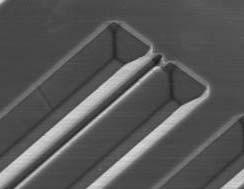

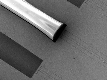


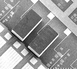

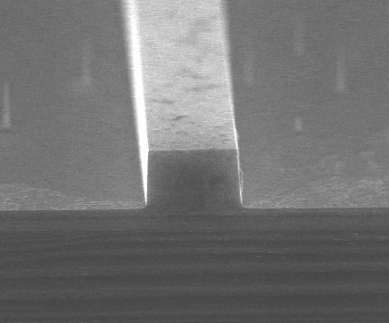

16 Micromachining for Packaging Use standard pick and place technologies along with litho defined silicon micromaching U-Grooves Tapers Mirror V-Grooves Laser Attach 45 Mirrors Facet Preparation *Third party marks and brands are the property of their respective owner 16
17 Intel s s Silicon Photonics Research 1. Develop photonic building blocks in silicon 2. Integrate increasing functionality directly onto silicon Integrated in Silicon Photodetectors DEMUX Receiver Chip Taper Driver Chip Passive Align Lasers MUX *Third party marks and brands are the property of their respective owner 17


18 Intel s s Silicon Photonics Research 1. Develop photonic building blocks in silicon 2. Integrate increasing functionality directly onto silicon 3. Long term explore monolithic integration Filter ECL Drivers Modulator Multiple Channels CMOS Circuitry TIA TIA Passive Alignment Photodetector *Third party marks and brands are the property of their respective owner 18
19 SILICON LASER What We announced on Feb 17th Research Breakthrough:1st Continuous Silicon Laser Silicon laser cavity on a single chip Published in the journal Nature on February 17, 2005 *Third party marks and brands are the property of their respective owner 19


20 The First Laser Developed by Ted Maiman, published in Nature,, August 6, this ruby laser used a flash lamp as an optical pump Fully Reflective Mirror Flash Lamp Partially Reflective Mirror RUBY CRYSTAL ROD LASER BEAM *Third party marks and brands are the property of their respective owner 20


21 Raman: (Historical Note) Raman Effect or Raman Scattering: A phenomenon observed in the scattering of light as it passes through a transparent medium; the light undergoes a change in frequency and random alteration in phase due to a change in rotational or vibrational energy of the scattering molecules. Discovered a material effect that is named after him Nature published his paper on the effect on March 31, 1928 He received the Nobel prize in 1930 for his discovery The first laser using the Raman effect was built in 1962 Today Raman based amplifiers are used throughout telecom Most long distance phone calls will go through a Raman amplifier Typical Raman Amplifier *Third party marks and brands are the property of their respective owner 21
22 Silicon Indium Antimonide (III-V) Quartz Lithium Niobate (used for modulators) Diamond Glass Fiber (Raman lasers/amps) The Raman Effect Materials Raman gain coefficient (10-8 m/mw) Kilometers of fiber... The Raman effect is 10,000 times stronger in silicon than in glass fiber Centimeters of silicon This allows for significant gain in centimeters instead of kilometers Fabrication of low-loss silicon waveguides is challenging *Third party marks and brands are the property of their respective owner 22


23 Raman Amplification Light from a pump beam exchanges energy with vibrating silicon atoms, causing energy to be transferred to the Raman wavelength. Passing an optical signal at this wavelength causes amplification. Pump Beam DATA beam At Raman wavelength Silicon Waveguide Raman Light Amplified DATA beam *Third party marks and brands are the property of their respective owner 23
24 Raman Gain in Silicon Silicon Waveguide Pump in Pump out Pump/probe experiment Probe in Probe out Raman Gain and WG loss vs. Input Pump Power -0.2 Raman gain (db) Input pump power(mw) (b) Raman Gain/WG Loss (db) Pump Power (mw) Gain-Loss (db) Raman Gain WG Loss Loss w/o Pump Gain-Loss CW Gain Saturation due to TPA induced FCA *Third party marks and brands are the property of their respective owner 24
25 Two Photon Absorption in Silicon Conduction band Pump λ=1.55μm Silicon band gap 1.1 ev Valence band Two photons can simultaneously hit an atom Combined energy enough to kick free an electron *Third party marks and brands are the property of their respective owner 25
26 Two Photon Absorption In silicon, one infrared photon doesn't have the energy to free an electron e e e e e e e e Free Electron e SILICON WAVEGUIDE But, occasionally, two photons can knock an electron out of orbit. Free electrons absorb individual photons and cancel Raman gain *Third party marks and brands are the property of their respective owner 26


27 Overcoming TPA induced FCA V + laser beam Raman Gain Gain needed to make a laser oxide p-type silicon electrons Gain limit due to Two Photon Absorption problem intrinsic silicon n-type silicon Pump power *Third party marks and brands are the property of their respective owner 27
 500 400 300 200 100 Lifetime=16 ns Lifetime=6.8 ns Lifetime=3.")
 TPA coeff ~ 0.5 cm/gw, α 0.39 db/cm, FCA cross sect 1.")
28 Effective Carrier lifetime reduction SiO 2 passivation Al contact Si rib waveguide p-region Buried oxide H W h Al contact n-region Output power (mw) Lifetime=16 ns Lifetime=6.8 ns Lifetime=3.2 ns Lifetime=1 ns 25 V 5 V short open Si substrate PIN Cross-section *Third party marks and brands are the property of their respective owner Input power (mw) TPA coeff ~ 0.5 cm/gw, α 0.39 db/cm, FCA cross sect 1.45e nm. The lifetime is used as a fitting parameter
29 CW gain vs. reverse bias voltage R. Jones et al. Optics Express 13 ( ) 525) 2005 NET GAIN NO NET GAIN Pump λ=1550 nm Signal λ=1686 nm *Third party marks and brands are the property of their respective owner 29
30 With gain can build Laser: Silicon Waveguide Cavity R f V bias 16 mm n-region R b Pump beam SOI rib waveguide 2 mm Laser output Dichroic coating p-region Broad-band reflective coating 24%/71% 90% *Third party marks and brands are the property of their respective owner 30

31 Animation Click in box while in slide show mode to start Click outside animation box after animation *Third party marks and brands are the property of their respective owner 31
32 Experimental setup Pump at 1,550 nm 0-10 Optical spectrum analyzer -80 Pump power monitor 90/10 Tap coupler Laser output power meter Polarization controller LP filter 90/10 Tap coupler Lensed fibre De-multiplexer Laser output at 1,686 nm Silicon waveguide Dichroic coating High reflection coating *Third party marks and brands are the property of their respective owner 32


33 Experimental Set up Test chip with 8 laser WG s Laser chip *Third party marks and brands are the property of their respective owner 33
34 Typical Lasing Criteria Threshold behavior: rapid growth in output power when gain > loss Spectral linewidth narrowing: Coherent light emission *Third party marks and brands are the property of their respective owner 34
35 Threshold, Efficiency, and PIN effect Laser output (mw) V bias 5V bias 25V slope 5V slope Coupled pump power (mw) Laser turns on at threshold, when gain per pass in cavity becomes greater than the loss. *Third party marks and brands are the property of their respective owner 35
36 Spontaneous emission vs. laser spectrum Spectral power (a. u.) Lasing signal Spontaneous emmission Magnified 10^ 5x Wavelength (nm) When lasing, the spectrum becomes much more narrow and much higher in power. *Third party marks and brands are the property of their respective owner 36
37 Wavelength tuning (comparison) 0-10 pump 0-10 Spactral power (db) nm 1550 nm 1552 nm 1554 nm 1556 nm 1558 nm Spactral power (db) nm 1550 nm 1552 nm 1554 nm 1556 nm 1558 nm Laser wavelength (nm) Laser wavelength (nm) Silicon Raman laser Commercial ECDL *Third party marks and brands are the property of their respective owner 37
38 Potential Applications *Third party marks and brands are the property of their respective owner 38

39 Communications Applications PUMP LASER passively aligned Si Raman Amplifier weak data beam waveguide coupler amplified data beam silicon waveguide (cm s) Si Multi-Channel Transmitter laser cavity modulators P passively aligned MOD PUMP LASER MOD MUX N splitter MOD MOD Optical Fiber Si Raman Modulator integrated mirrors *Third party marks and brands are the property of their respective owner 39


40 Covering the Gaps Different wavelengths require different types of lasers Mid-Infrared very difficult for compact semiconductors Raman Lasers could enable lasers at these wavelengths Applications in sensing, analysis, medicine, and others 2.1µm Ho:YAG laser Compact Semi. Lasers PUMP LASER 2.9µm Er:YAG laser cascaded mirrors >2µm Could enable lasers for a variety of applications *Third party marks and brands are the property of their respective owner 40
41 Summary Long term convergence opportunities are with silicon B/W will continue drive conversion of optical into interconnects Tremendous progress from research community Need to continue pushing & improving performance Integration is next set of challenges Will be challenging but will bring new functionality and form factors In order to benefit Technologies must be CMOS compatible to benefit from HVM & infrastructure Silicon will not win with individual devices, but with integrated modules that bring increased total functionality & intelligence at a lower cost *Third party marks and brands are the property of their respective owner 41
42 Backup.. *Third party marks and brands are the property of their respective owner 42
Silicon Photonics Opportunity, Applicatoins & Recent Results. Mario Paniccia, Director Photonics Technology Lab Intel Corporation
 Silicon Photonics Opportunity, Applicatoins & Recent Results Mario Paniccia, Director Photonics Technology Lab Intel Corporation Intel Corporation CREOL April 1 2005 Agenda Opportunity for Silicon Photonics
Silicon Photonics Opportunity, applications & Recent Results
 Silicon Photonics Opportunity, applications & Recent Results Dr. Mario Paniccia Intel Fellow Director, Photonics Technology Lab Intel Corporation www.intel.com/go/sp Purdue University Oct 5 2007 Agenda
A continuous-wave Raman silicon laser
 A continuous-wave Raman silicon laser Haisheng Rong, Richard Jones,.. - Intel Corporation Ultrafast Terahertz nanoelectronics Lab Jae-seok Kim 1 Contents 1. Abstract 2. Background I. Raman scattering II.
Silicon Photonics Photo-Detector Announcement. Mario Paniccia Intel Fellow Director, Photonics Technology Lab
 Silicon Photonics Photo-Detector Announcement Mario Paniccia Intel Fellow Director, Photonics Technology Lab Agenda Intel s Silicon Photonics Research 40G Modulator Recap 40G Photodetector Announcement
Low threshold continuous wave Raman silicon laser
 NATURE PHOTONICS, VOL. 1, APRIL, 2007 Low threshold continuous wave Raman silicon laser HAISHENG RONG 1 *, SHENGBO XU 1, YING-HAO KUO 1, VANESSA SIH 1, ODED COHEN 2, OMRI RADAY 2 AND MARIO PANICCIA 1 1:
Optodevice Data Book ODE I. Rev.9 Mar Opnext Japan, Inc.
 Optodevice Data Book ODE-408-001I Rev.9 Mar. 2003 Opnext Japan, Inc. Section 1 Operating Principles 1.1 Operating Principles of Laser Diodes (LDs) and Infrared Emitting Diodes (IREDs) 1.1.1 Emitting Principles
Four wave mixing and parametric amplification in Si-nano waveguides using reverse biased pnjunctions
 Four wave mixing and parametric amplification in Si-nano waveguides using reverse biased pnjunctions for carrier removal E-Mail: petermann@tu-berlin.de Acknowledgements A.Gajda 1, G.Winzer 1, L.Zimmermann
Electronic-Photonic ICs for Low Cost and Scalable Datacenter Solutions
 Electronic-Photonic ICs for Low Cost and Scalable Datacenter Solutions Christoph Theiss, Director Packaging Christoph.Theiss@sicoya.com 1 SEMICON Europe 2016, October 27 2016 Sicoya Overview Spin-off from
Si CMOS Technical Working Group
 Si CMOS Technical Working Group CTR, Spring 2008 meeting Markets Interconnects TWG Breakouts Reception TWG reports Si CMOS: photonic integration E-P synergy - Integration - Standardization - Cross-market
Lecture: Integration of silicon photonics with electronics. Prepared by Jean-Marc FEDELI CEA-LETI
 Lecture: Integration of silicon photonics with electronics Prepared by Jean-Marc FEDELI CEA-LETI Context The goal is to give optical functionalities to electronics integrated circuit (EIC) The objectives
Optical Amplifiers Photonics and Integrated Optics (ELEC-E3240) Zhipei Sun Photonics Group Department of Micro- and Nanosciences Aalto University
 Zhipei Sun Photonics Group Department of Micro- and Nanosciences Aalto University") Photonics Group Department of Micro- and Nanosciences Aalto University Optical Amplifiers Photonics and Integrated Optics (ELEC-E3240) Zhipei Sun Last Lecture Topics Course introduction Ray optics & optical
Photonics Group Department of Micro- and Nanosciences Aalto University Optical Amplifiers Photonics and Integrated Optics (ELEC-E3240) Zhipei Sun Last Lecture Topics Course introduction Ray optics & optical
A 3.9 ns 8.9 mw 4 4 Silicon Photonic Switch Hybrid-Integrated with CMOS Driver
 A 3.9 ns 8.9 mw 4 4 Silicon Photonic Switch Hybrid-Integrated with CMOS Driver A. Rylyakov, C. Schow, B. Lee, W. Green, J. Van Campenhout, M. Yang, F. Doany, S. Assefa, C. Jahnes, J. Kash, Y. Vlasov IBM
Lecture 6 Fiber Optical Communication Lecture 6, Slide 1
 Lecture 6 Optical transmitters Photon processes in light matter interaction Lasers Lasing conditions The rate equations CW operation Modulation response Noise Light emitting diodes (LED) Power Modulation
Optical Amplifiers. Continued. Photonic Network By Dr. M H Zaidi
 Optical Amplifiers Continued EDFA Multi Stage Designs 1st Active Stage Co-pumped 2nd Active Stage Counter-pumped Input Signal Er 3+ Doped Fiber Er 3+ Doped Fiber Output Signal Optical Isolator Optical
Introduction Fundamental of optical amplifiers Types of optical amplifiers
 ECE 6323 Introduction Fundamental of optical amplifiers Types of optical amplifiers Erbium-doped fiber amplifiers Semiconductor optical amplifier Others: stimulated Raman, optical parametric Advanced application:
IBM T. J. Watson Research Center IBM Corporation
 Broadband Silicon Photonic Switch Integrated with CMOS Drive Electronics B. G. Lee, J. Van Campenhout, A. V. Rylyakov, C. L. Schow, W. M. J. Green, S. Assefa, M. Yang, F. E. Doany, C. V. Jahnes, R. A.
Microphotonics Readiness for Commercial CMOS Manufacturing. Marco Romagnoli
 Microphotonics Readiness for Commercial CMOS Manufacturing Marco Romagnoli MicroPhotonics Consortium meeting MIT, Cambridge October 15 th, 2012 Passive optical structures based on SOI technology Building
Introduction Fundamentals of laser Types of lasers Semiconductor lasers
 ECE 5368 Introduction Fundamentals of laser Types of lasers Semiconductor lasers Introduction Fundamentals of laser Types of lasers Semiconductor lasers How many types of lasers? Many many depending on
NEXT GENERATION SILICON PHOTONICS FOR COMPUTING AND COMMUNICATION PHILIPPE ABSIL
 NEXT GENERATION SILICON PHOTONICS FOR COMPUTING AND COMMUNICATION PHILIPPE ABSIL OUTLINE Introduction Platform Overview Device Library Overview What s Next? Conclusion OUTLINE Introduction Platform Overview
Trends in Optical Transceivers:
 Trends in Optical Transceivers: Light sources for premises networks Peter Ronco Corning Optical Fiber Asst. Product Line Manager Premises Fibers January 24, 2006 Outline: Introduction: Transceivers and
Light source approach for silicon photonics transceivers September Fiber to the Chip
 Light source approach for silicon photonics transceivers September 2014 Fiber to the Chip Silicon Photonics Silicon Photonics Technology: Silicon material system & processing techniques to manufacture
Lecture 4 INTEGRATED PHOTONICS
 Lecture 4 INTEGRATED PHOTONICS What is photonics? Photonic applications use the photon in the same way that electronic applications use the electron. Devices that run on light have a number of advantages
Silicon Photonics: A Platform for Integration, Wafer Level Assembly and Packaging
 Silicon Photonics: A Platform for Integration, Wafer Level Assembly and Packaging M. Asghari Kotura Inc April 27 Contents: Who is Kotura Choice of waveguide technology Challenges and merits of Si photonics
Convergence Challenges of Photonics with Electronics
 Convergence Challenges of Photonics with Electronics Edward Palen, Ph.D., P.E. PalenSolutions - Optoelectronic Packaging Consulting www.palensolutions.com palensolutions@earthlink.net 415-850-8166 October
Photonics and Optical Communication Spring 2005
 Photonics and Optical Communication Spring 2005 Final Exam Instructor: Dr. Dietmar Knipp, Assistant Professor of Electrical Engineering Name: Mat. -Nr.: Guidelines: Duration of the Final Exam: 2 hour You
InP-based Waveguide Photodetector with Integrated Photon Multiplication
 InP-based Waveguide Photodetector with Integrated Photon Multiplication D.Pasquariello,J.Piprek,D.Lasaosa,andJ.E.Bowers Electrical and Computer Engineering Department University of California, Santa Barbara,
Index. Cambridge University Press Silicon Photonics Design Lukas Chrostowski and Michael Hochberg. Index.
 absorption, 69 active tuning, 234 alignment, 394 396 apodization, 164 applications, 7 automated optical probe station, 389 397 avalanche detector, 268 back reflection, 164 band structures, 30 bandwidth
Silicon photonics with low loss and small polarization dependency. Timo Aalto VTT Technical Research Centre of Finland
 Silicon photonics with low loss and small polarization dependency Timo Aalto VTT Technical Research Centre of Finland EPIC workshop in Tokyo, 9 th November 2017 VTT Technical Research Center of Finland
New silicon photonics technology delivers faster data traffic in data centers
 Edition May 2017 Silicon Photonics, Photonics New silicon photonics technology delivers faster data traffic in data centers New transceiver with 10x higher bandwidth than current transceivers. Today, the
Silicon Photonics Michael R. Bynum Physics 464: Applied Optics Winter 2006
 Silicon Photonics Michael R. Bynum Physics 464: Applied Optics Winter 2006 Abstract Copper interconnects will soon be the limiting factor of the performance of a computer. The aim of Silicon Photonics
Silicon Photonics Technology Platform To Advance The Development Of Optical Interconnects
 Silicon Photonics Technology Platform To Advance The Development Of Optical Interconnects By Mieke Van Bavel, science editor, imec, Belgium; Joris Van Campenhout, imec, Belgium; Wim Bogaerts, imec s associated
Ph 77 ADVANCED PHYSICS LABORATORY ATOMIC AND OPTICAL PHYSICS
 Ph 77 ADVANCED PHYSICS LABORATORY ATOMIC AND OPTICAL PHYSICS Diode Laser Characteristics I. BACKGROUND Beginning in the mid 1960 s, before the development of semiconductor diode lasers, physicists mostly
S Optical Networks Course Lecture 2: Essential Building Blocks
 S-72.3340 Optical Networks Course Lecture 2: Essential Building Blocks Edward Mutafungwa Communications Laboratory, Helsinki University of Technology, P. O. Box 2300, FIN-02015 TKK, Finland Tel: +358 9
Optical Receivers Theory and Operation
 Optical Receivers Theory and Operation Photo Detectors Optical receivers convert optical signal (light) to electrical signal (current/voltage) Hence referred O/E Converter Photodetector is the fundamental
Vertical External Cavity Surface Emitting Laser
 Chapter 4 Optical-pumped Vertical External Cavity Surface Emitting Laser The booming laser techniques named VECSEL combine the flexibility of semiconductor band structure and advantages of solid-state
Luminous Equivalent of Radiation
 Intensity vs λ Luminous Equivalent of Radiation When the spectral power (p(λ) for GaP-ZnO diode has a peak at 0.69µm) is combined with the eye-sensitivity curve a peak response at 0.65µm is obtained with
CHAPTER 2 POLARIZATION SPLITTER- ROTATOR BASED ON A DOUBLE- ETCHED DIRECTIONAL COUPLER
 CHAPTER 2 POLARIZATION SPLITTER- ROTATOR BASED ON A DOUBLE- ETCHED DIRECTIONAL COUPLER As we discussed in chapter 1, silicon photonics has received much attention in the last decade. The main reason is
PLC-based integrated devices for advanced modulation formats
 ECOC 2009 workshop 7-5 Sep. 20, 2009 PLC-based integrated devices for advanced modulation formats Y. Inoue NTT Photonics Labs. NTT Corporation NTT Photonics Laboratories Hybrid integration of photonics
Chapter 8. Wavelength-Division Multiplexing (WDM) Part II: Amplifiers
 Part II: Amplifiers") Chapter 8 Wavelength-Division Multiplexing (WDM) Part II: Amplifiers Introduction Traditionally, when setting up an optical link, one formulates a power budget and adds repeaters when the path loss exceeds
Chapter 8 Wavelength-Division Multiplexing (WDM) Part II: Amplifiers Introduction Traditionally, when setting up an optical link, one formulates a power budget and adds repeaters when the path loss exceeds
High-speed Ge photodetector monolithically integrated with large cross silicon-on-insulator waveguide
 [ APPLIED PHYSICS LETTERS ] High-speed Ge photodetector monolithically integrated with large cross silicon-on-insulator waveguide Dazeng Feng, Shirong Liao, Roshanak Shafiiha. etc Contents 1. Introduction
Silicon photonics on 3 and 12 μm thick SOI for optical interconnects Timo Aalto VTT Technical Research Centre of Finland
 Silicon photonics on 3 and 12 μm thick SOI for optical interconnects Timo Aalto VTT Technical Research Centre of Finland 5th International Symposium for Optical Interconnect in Data Centres in ECOC, Gothenburg,
Spectroscopy of Ruby Fluorescence Physics Advanced Physics Lab - Summer 2018 Don Heiman, Northeastern University, 1/12/2018
 1 Spectroscopy of Ruby Fluorescence Physics 3600 - Advanced Physics Lab - Summer 2018 Don Heiman, Northeastern University, 1/12/2018 I. INTRODUCTION The laser was invented in May 1960 by Theodor Maiman.
R. J. Jones Optical Sciences OPTI 511L Fall 2017
 R. J. Jones Optical Sciences OPTI 511L Fall 2017 Semiconductor Lasers (2 weeks) Semiconductor (diode) lasers are by far the most widely used lasers today. Their small size and properties of the light output
Application Instruction 002. Superluminescent Light Emitting Diodes: Device Fundamentals and Reliability
 I. Introduction II. III. IV. SLED Fundamentals SLED Temperature Performance SLED and Optical Feedback V. Operation Stability, Reliability and Life VI. Summary InPhenix, Inc., 25 N. Mines Road, Livermore,
Nd: YAG Laser Energy Levels 4 level laser Optical transitions from Ground to many upper levels Strong absorber in the yellow range None radiative to
 Nd: YAG Lasers Dope Neodynmium (Nd) into material (~1%) Most common Yttrium Aluminum Garnet - YAG: Y 3 Al 5 O 12 Hard brittle but good heat flow for cooling Next common is Yttrium Lithium Fluoride: YLF
DBR based passively mode-locked 1.5m semiconductor laser with 9 nm tuning range Moskalenko, V.; Williams, K.A.; Bente, E.A.J.M.
 DBR based passively mode-locked 1.5m semiconductor laser with 9 nm tuning range Moskalenko, V.; Williams, K.A.; Bente, E.A.J.M. Published in: Proceedings of the 20th Annual Symposium of the IEEE Photonics
Fiberoptic Communication Systems By Dr. M H Zaidi. Optical Amplifiers
 Optical Amplifiers Optical Amplifiers Optical signal propagating in fiber suffers attenuation Optical power level of a signal must be periodically conditioned Optical amplifiers are a key component in
FIBER OPTICS. Prof. R.K. Shevgaonkar. Department of Electrical Engineering. Indian Institute of Technology, Bombay. Lecture: 18.
 FIBER OPTICS Prof. R.K. Shevgaonkar Department of Electrical Engineering Indian Institute of Technology, Bombay Lecture: 18 Optical Sources- Introduction to LASER Diodes Fiber Optics, Prof. R.K. Shevgaonkar,
The Past, Present, and Future of Silicon Photonics
 The Past, Present, and Future of Silicon Photonics Myung-Jae Lee High-Speed Circuits & Systems Lab. Dept. of Electrical and Electronic Engineering Yonsei University Outline Introduction A glance at history
Photo-Electronic Crossbar Switching Network for Multiprocessor Systems
 Photo-Electronic Crossbar Switching Network for Multiprocessor Systems Atsushi Iwata, 1 Takeshi Doi, 1 Makoto Nagata, 1 Shin Yokoyama 2 and Masataka Hirose 1,2 1 Department of Physical Electronics Engineering
Integrated electro-optical waveguide based devices with liquid crystals on a silicon backplane
 Integrated electro-optical waveguide based devices with liquid crystals on a silicon backplane Florenta Costache Group manager Smart Micro-Optics SMO/AMS Fraunhofer Institute for Photonic Microsystems,
Optical Fibre Amplifiers Continued
 1 Optical Fibre Amplifiers Continued Stavros Iezekiel Department of Electrical and Computer Engineering University of Cyprus ECE 445 Lecture 09 Fall Semester 2016 2 ERBIUM-DOPED FIBRE AMPLIFIERS BASIC
UNMATCHED OUTPUT POWER AND TUNING RANGE
 ARGOS MODEL 2400 SF SERIES TUNABLE SINGLE-FREQUENCY MID-INFRARED SPECTROSCOPIC SOURCE UNMATCHED OUTPUT POWER AND TUNING RANGE One of Lockheed Martin s innovative laser solutions, Argos TM Model 2400 is
Transmitting Light: Fiber-optic and Free-space Communications Holography
 1 Lecture 9 Transmitting Light: Fiber-optic and Free-space Communications Holography 2 Wireless Phone Calls http://havilandtelconews.com/2011/10/the-reality-behind-wireless-networks/ 3 Undersea Cable and
High brightness semiconductor lasers M.L. Osowski, W. Hu, R.M. Lammert, T. Liu, Y. Ma, S.W. Oh, C. Panja, P.T. Rudy, T. Stakelon and J.E.
 QPC Lasers, Inc. 2007 SPIE Photonics West Paper: Mon Jan 22, 2007, 1:20 pm, LASE Conference 6456, Session 3 High brightness semiconductor lasers M.L. Osowski, W. Hu, R.M. Lammert, T. Liu, Y. Ma, S.W. Oh,
Integrated disruptive components for 2µm fibre Lasers ISLA. 2 µm Sub-Picosecond Fiber Lasers
 Integrated disruptive components for 2µm fibre Lasers ISLA 2 µm Sub-Picosecond Fiber Lasers Advantages: 2 - microns wavelength offers eye-safety potentially higher pulse energy and average power in single
Examination Optoelectronic Communication Technology. April 11, Name: Student ID number: OCT1 1: OCT 2: OCT 3: OCT 4: Total: Grade:
 Examination Optoelectronic Communication Technology April, 26 Name: Student ID number: OCT : OCT 2: OCT 3: OCT 4: Total: Grade: Declaration of Consent I hereby agree to have my exam results published on
- no emitters/amplifiers available. - complex process - no CMOS-compatible
 Advantages of photonic integrated circuits (PICs) in Microwave Photonics (MWP): compactness low-power consumption, stability flexibility possibility of aggregating optics and electronics functionalities
OPTICAL NETWORKS. Building Blocks. A. Gençata İTÜ, Dept. Computer Engineering 2005
 OPTICAL NETWORKS Building Blocks A. Gençata İTÜ, Dept. Computer Engineering 2005 Introduction An introduction to WDM devices. optical fiber optical couplers optical receivers optical filters optical amplifiers
OPTI510R: Photonics. Khanh Kieu College of Optical Sciences, University of Arizona Meinel building R.626
 OPTI510R: Photonics Khanh Kieu College of Optical Sciences, University of Arizona kkieu@optics.arizona.edu Meinel building R.626 Announcements Homework #3 is due today No class Monday, Feb 26 Pre-record
Quantum-Well Semiconductor Saturable Absorber Mirror
 Chapter 3 Quantum-Well Semiconductor Saturable Absorber Mirror The shallow modulation depth of quantum-dot saturable absorber is unfavorable to increasing pulse energy and peak power of Q-switched laser.
The Light at the End of the Wire. Dana Vantrease + HP Labs + Mikko Lipasti
 The Light at the End of the Wire Dana Vantrease + HP Labs + Mikko Lipasti 1 Goals of This Talk Why should we (architects) be interested in optics? How does on-chip optics work? What can we build with optics?
Integration of Optoelectronic and RF Devices for Applications in Optical Interconnect and Wireless Communication
 Integration of Optoelectronic and RF Devices for Applications in Optical Interconnect and Wireless Communication Zhaoran (Rena) Huang Assistant Professor Department of Electrical, Computer and System Engineering
A novel tunable diode laser using volume holographic gratings
 A novel tunable diode laser using volume holographic gratings Christophe Moser *, Lawrence Ho and Frank Havermeyer Ondax, Inc. 85 E. Duarte Road, Monrovia, CA 9116, USA ABSTRACT We have developed a self-aligned
A new picosecond Laser pulse generation method.
 PULSE GATING : A new picosecond Laser pulse generation method. Picosecond lasers can be found in many fields of applications from research to industry. These lasers are very common in bio-photonics, non-linear
Semiconductor Optical Communication Components and Devices Lecture 18: Introduction to Diode Lasers - I
 Semiconductor Optical Communication Components and Devices Lecture 18: Introduction to Diode Lasers - I Prof. Utpal Das Professor, Department of lectrical ngineering, Laser Technology Program, Indian Institute
External Cavity Diode Laser Tuned with Silicon MEMS
 External Cavity Diode Laser Tuned with Silicon MEMS MEMS-Tunable External Cavity Diode Laser Lenses Laser Output Diffraction Grating AR-coated FP Diode Silicon Mirror 3 mm Balanced MEMS Actuator iolon
Elimination of Self-Pulsations in Dual-Clad, Ytterbium-Doped Fiber Lasers
 Elimination of Self-Pulsations in Dual-Clad, Ytterbium-Doped Fiber Lasers 1.0 Modulation depth 0.8 0.6 0.4 0.2 0.0 Laser 3 Laser 2 Laser 4 2 3 4 5 6 7 8 Absorbed pump power (W) Laser 1 W. Guan and J. R.
Silicon photonics integration roadmap for applications in computing systems
 Silicon photonics integration roadmap for applications in computing systems Bert Jan Offrein Neuromorphic Devices and Systems Group 2016 IBM Corporation Outline Photonics and computing? The interconnect
3550 Aberdeen Ave SE, Kirtland AFB, NM 87117, USA ABSTRACT 1. INTRODUCTION
 Beam Combination of Multiple Vertical External Cavity Surface Emitting Lasers via Volume Bragg Gratings Chunte A. Lu* a, William P. Roach a, Genesh Balakrishnan b, Alexander R. Albrecht b, Jerome V. Moloney
Frequency Noise Reduction of Integrated Laser Source with On-Chip Optical Feedback
 MITSUBISHI ELECTRIC RESEARCH LABORATORIES http://www.merl.com Frequency Noise Reduction of Integrated Laser Source with On-Chip Optical Feedback Song, B.; Kojima, K.; Pina, S.; Koike-Akino, T.; Wang, B.;
Silicon-On-Insulator based guided wave optical clock distribution
 Silicon-On-Insulator based guided wave optical clock distribution K. E. Moselund, P. Dainesi, and A. M. Ionescu Electronics Laboratory Swiss Federal Institute of Technology People and funding EPFL Project
! Couplers. ! Isolators/Circulators. ! Multiplexers/Filters. ! Optical Amplifiers. ! Transmitters (lasers,leds) ! Detectors (receivers) !
 ! Detectors (receivers) !") Components of Optical Networks Based on: Rajiv Ramaswami, Kumar N. Sivarajan, Optical Networks A Practical Perspective 2 nd Edition, 2001 October, Morgan Kaufman Publishers Optical Components! Couplers!
Components of Optical Networks Based on: Rajiv Ramaswami, Kumar N. Sivarajan, Optical Networks A Practical Perspective 2 nd Edition, 2001 October, Morgan Kaufman Publishers Optical Components! Couplers!
Silicon Photonics in Optical Communications. Lars Zimmermann, IHP, Frankfurt (Oder), Germany
, Germany") Silicon Photonics in Optical Communications Lars Zimmermann, IHP, Frankfurt (Oder), Germany Outline IHP who we are Silicon photonics Photonic-electronic integration IHP photonic technology Conclusions
Silicon Photonics in Optical Communications Lars Zimmermann, IHP, Frankfurt (Oder), Germany Outline IHP who we are Silicon photonics Photonic-electronic integration IHP photonic technology Conclusions
Heterogeneously Integrated Microwave Signal Generators with Narrow- Linewidth Lasers
 Heterogeneously Integrated Microwave Signal Generators with Narrow- Linewidth Lasers John E. Bowers, Jared Hulme, Tin Komljenovic, Mike Davenport and Chong Zhang Department of Electrical and Computer Engineering
Opto-VLSI-based reconfigurable photonic RF filter
 Research Online ECU Publications 29 Opto-VLSI-based reconfigurable photonic RF filter Feng Xiao Mingya Shen Budi Juswardy Kamal Alameh This article was originally published as: Xiao, F., Shen, M., Juswardy,
Doppler-Free Spetroscopy of Rubidium
 Doppler-Free Spetroscopy of Rubidium Pranjal Vachaspati, Sabrina Pasterski MIT Department of Physics (Dated: April 17, 2013) We present a technique for spectroscopy of rubidium that eliminates doppler
EPIC: The Convergence of Electronics & Photonics
 EPIC: The Convergence of Electronics & Photonics K-Y Tu, Y.K. Chen, D.M. Gill, M. Rasras, S.S. Patel, A.E. White ell Laboratories, Lucent Technologies M. Grove, D.C. Carothers, A.T. Pomerene, T. Conway
Hybrid Integration Technology of Silicon Optical Waveguide and Electronic Circuit
 Hybrid Integration Technology of Silicon Optical Waveguide and Electronic Circuit Daisuke Shimura Kyoko Kotani Hiroyuki Takahashi Hideaki Okayama Hiroki Yaegashi Due to the proliferation of broadband services
IEEE JOURNAL OF SELECTED TOPICS IN QUANTUM ELECTRONICS 2010 Silicon Photonic Circuits: On-CMOS Integration, Fiber Optical Coupling, and Packaging
 IEEE JOURNAL OF SELECTED TOPICS IN QUANTUM ELECTRONICS 2010 Silicon Photonic Circuits: On-CMOS Integration, Fiber Optical Coupling, and Packaging Christophe Kopp, St ephane Bernab e, Badhise Ben Bakir,
InP-based Waveguide Photodetector with Integrated Photon Multiplication
 InP-based Waveguide Photodetector with Integrated Photon Multiplication D.Pasquariello,J.Piprek,D.Lasaosa,andJ.E.Bowers Electrical and Computer Engineering Department University of California, Santa Barbara,
Semiconductor Optoelectronics Prof. M. R. Shenoy Department of Physics Indian Institute of Technology, Delhi
 Semiconductor Optoelectronics Prof. M. R. Shenoy Department of Physics Indian Institute of Technology, Delhi Lecture - 26 Semiconductor Optical Amplifier (SOA) (Refer Slide Time: 00:39) Welcome to this
This writeup is adapted from Fall 2002, final project report for by Robert Winsor.
 Optical Waveguides in Andreas G. Andreou This writeup is adapted from Fall 2002, final project report for 520.773 by Robert Winsor. September, 2003 ABSTRACT This lab course is intended to give students
Lecture 1: Course Overview. Rajeev J. Ram
 Lecture 1: Course Overview Rajeev J. Ram Office: 36-491 Telephone: X3-4182 Email: rajeev@mit.edu Syllabus Basic concepts Advanced concepts Background: p-n junctions Photodetectors Modulators Optical amplifiers
Graphene electro-optic modulator with 30 GHz bandwidth
 Graphene electro-optic modulator with 30 GHz bandwidth Christopher T. Phare 1, Yoon-Ho Daniel Lee 1, Jaime Cardenas 1, and Michal Lipson 1,2,* 1School of Electrical and Computer Engineering, Cornell University,
Introduction and concepts Types of devices
 ECE 6323 Introduction and concepts Types of devices Passive splitters, combiners, couplers Wavelength-based devices for DWDM Modulator/demodulator (amplitude and phase), compensator (dispersion) Others:
A Comparison of Optical Modulator Structures Using a Matrix Simulation Approach
 A Comparison of Optical Modulator Structures Using a Matrix Simulation Approach Kjersti Kleven and Scott T. Dunham Department of Electrical Engineering University of Washington 27 September 27 Outline
Survey Report: Laser R&D
 Survey Report: Laser R&D Peter Moulton VP/CTO, Q-Peak, Inc. DLA-2011 ICFA Mini-Workshop on Dielectric Laser Accelerators September 15, 2011 SLAC, Menlo Park, CA Outline DLA laser requirements (one version)
Optical Fiber Amplifiers. Scott Freese. Physics May 2008
 Optical Fiber Amplifiers Scott Freese Physics 262 2 May 2008 Partner: Jared Maxson Abstract The primary goal of this experiment was to gain an understanding of the basic components of an Erbium doped fiber
Impact of High-Speed Modulation on the Scalability of Silicon Photonic Interconnects
 Impact of High-Speed Modulation on the Scalability of Silicon Photonic Interconnects OPTICS 201, March 18 th, Dresden, Germany Meisam Bahadori, Sébastien Rumley,and Keren Bergman Lightwave Research Lab,
ECEN689: Special Topics in Optical Interconnects Circuits and Systems Spring 2016
 ECEN689: Special Topics in Optical Interconnects Circuits and Systems Spring 2016 Lecture 10: Electroabsorption Modulator Transmitters Sam Palermo Analog & Mixed-Signal Center Texas A&M University Announcements
Laser Diode. Photonic Network By Dr. M H Zaidi
 Laser Diode Light emitters are a key element in any fiber optic system. This component converts the electrical signal into a corresponding light signal that can be injected into the fiber. The light emitter
Silicon nitride based TriPleX Photonic Integrated Circuits for sensing applications
 Silicon nitride based TriPleX Photonic Integrated Circuits for sensing applications Arne Leinse a.leinse@lionix-int.com 2 Our chips drive your business 2 What are Photonic ICs (PICs)? Photonic Integrated
Chapter 12: Optical Amplifiers: Erbium Doped Fiber Amplifiers (EDFAs)
") Chapter 12: Optical Amplifiers: Erbium Doped Fiber Amplifiers (EDFAs) Prof. Dr. Yaocheng SHI ( 时尧成 ) yaocheng@zju.edu.cn http://mypage.zju.edu.cn/yaocheng 1 Traditional Optical Communication System Loss
Chapter 12: Optical Amplifiers: Erbium Doped Fiber Amplifiers (EDFAs) Prof. Dr. Yaocheng SHI ( 时尧成 ) yaocheng@zju.edu.cn http://mypage.zju.edu.cn/yaocheng 1 Traditional Optical Communication System Loss
Public Progress Report 2
 Embedded Resonant and ModulablE Self- Tuning Laser Cavity for Next Generation Access Network Transmitter ERMES Public Progress Report 2 Project Project acronym: ERMES Project full title: Embedded Resonant
Basic concepts. Optical Sources (b) Optical Sources (a) Requirements for light sources (b) Requirements for light sources (a)
 Optical Sources (a) Requirements for light sources (b) Requirements for light sources (a)") Optical Sources (a) Optical Sources (b) The main light sources used with fibre optic systems are: Light-emitting diodes (LEDs) Semiconductor lasers (diode lasers) Fibre laser and other compact solid-state
Optical Sources (a) Optical Sources (b) The main light sources used with fibre optic systems are: Light-emitting diodes (LEDs) Semiconductor lasers (diode lasers) Fibre laser and other compact solid-state
WWDM Transceiver Module for 10-Gb/s Ethernet
 WWDM Transceiver Module for 10-Gb/s Ethernet Brian E. Lemoff Hewlett-Packard Laboratories lemoff@hpl.hp.com IEEE 802.3 HSSG Interim Meeting Coeur d Alene, Idaho June 1-3, 1999 Why pursue WWDM for the LAN?
Waveguide-based single-pixel up-conversion infrared spectrometer
 Waveguide-based single-pixel up-conversion infrared spectrometer Qiang Zhang 1,2, Carsten Langrock 1, M. M. Fejer 1, Yoshihisa Yamamoto 1,2 1. Edward L. Ginzton Laboratory, Stanford University, Stanford,
Micro-sensors - what happens when you make "classical" devices "small": MEMS devices and integrated bolometric IR detectors
 Micro-sensors - what happens when you make "classical" devices "small": MEMS devices and integrated bolometric IR detectors Dean P. Neikirk 1 MURI bio-ir sensors kick-off 6/16/98 Where are the targets
PHOTONICS. Green Silicon
 Bahram Jalali, Sasan Fathpour and Kevin Tsia Green Silicon PHOTONICS Silicon photonics has shown great promise in overcoming communications bottlenecks and providing low-cost components for the Internet