Submicron SOI waveguides Dries Van Thourhout Trento 05
|
|
|
- Adam George
- 5 years ago
- Views:
Transcription
1 Submicron SOI waveguides Dries Van Thourhout Trento 05
 The Photonic Research Group at Ghent University IMEC Pieter Dumon, Wim")

2 Acknowledgements The European Union IST-PICCO and IST-PICMOS project The European Space Agency The Belgian IAP-PHOTON network The Flemish Institute for the industrial advancement of Scientific and Technological Research (IWT) The Photonic Research Group at Ghent University IMEC Pieter Dumon, Wim Bogaerts, Dries Van Thourhout, Dirk Taillaert, Bert Luyssaert, Peter Bienstman, Joris Van Campenhout, Gunther Roelkens, Ilse Christiaens The Silicon Process division at IMEC Vincent Wiaux, Stephan Beckx, Johan Wouters, Diziana Vangoidsenhoven, Rudi De Ruyter, Johan Mees 2
3 Outline Submicron SOI-wires Introduction: why do we need them Basic properties: design, loss, wavelength, polarization Fabrication Devices: couplers, crossings, filters III-V on Silicon Introduction Coupling of light Fabrication PICMOS (Photonic Interconnect on CMOS) 3
4 Scale difference Electronics interconnects gate transistor width flip-flop Active opto-electronics Wavelength-scale photonics LED VCSEL detector stripe laser 2R regenerator Passive photonics Wavelength-scale photonics fibre core linewidth in current PIC Bend radius taper spot-size convertor AWG in Silica on Silicon 100nm 1µm 10µm 100µm 1mm 1cm 4
5 PICs: today and future Today (InP, Silica-on-Silicon...): Size of components on a chip (both functional components and interconnect components): µm 2 Number of components on a chip: Future (10-20 years from now): Size of components on a chip (both functional components and interconnect components): µm 2 Number of components on a chip:
 http://photonics.intec.ugent.be 6")
6 Silica-on-silicon NTT (e.g. Miya e.a., IEEE STQE 00 pp.38) 6
7 Reduce PIC-size / increase density WE NEED: Ultra-compact waveguiding with Sharp bends (Bend radius < 10µm) Compact splitters and combiners Short mode-conversion distances Compact wavelength selective functions Highly dispersive element Small, high-q resonators Compact non-linear functions Increase power density by using tight confinement 7
8 High refractive index contrast (>2:1) High refractive index contrast allows for: Very tight bends Compact resonators with low loss Wide angle mirrors Very compact mode size strong field strength strong non-linear effects small volume to be pumped in active devices faster and/or lower power Photonic band gap effects air semiconductor dielectric High refractive index contrast is key for ultra-compact photonic circuits 8
9 Index Contrast Conventional PICs High Nanophotonics Out-of-plane index contrast Low Low In-plane (effective) index contrast High 9
10 Materials for nanophotonic waveguides In-plane index Out-of-plane contrast index contrast Si/SiO 2 (SOI) 3.5 to to 1.5 Si/air 3.5 to to 1 (membrane) GaAs/AlOx 3.5 to to 1.5 InP/SiO to to 1.5 SiON/SiO 2 2 to 1.5/1 2 to 1.5 GaAs/AlGaAs 3.5 to to 3.2 InGaAsP/InP 3.3 to to
11 SOI nanophotonics Width + Height Waveguide Definition Start: BOX SOI-Wafer thickness Thin Silicon layer Thick SiO 2 buffer 11
12 SOI-wires Group Date h [nm] w [nm] loss [db/cm] BOX [um] top clad Fab. IMEC Apr. ' no DUV IBM Apr. ' no EBeam Cornell Aug. ' no EBeam NTT Dec. ' no EBeam Yokohama Dec. ' no EBeam MIT Dec. ' yes G-line oxidation LETI / LPM Apr. ' yes DUV Columbia Oct yes EBeam (Table partly from Vlasov, McNab, Opt. Expr. 04, pp1630) 12
13 Outline Submicron SOI-wires Introduction: why do we need them Basic properties: theory, design, loss, wavelength, polarization Fabrication Devices: couplers, crossings, filters III-V on Silicon Introduction Coupling of light Fabrication PICMOS (Photonic Interconnect on CMOS) 13
14 Back to basics: cavities and waveguides How does light propagate in waveguides and cavities? n 2 n 2 n 1 n 1 Propagation in waveguide n 2 Emission within waveguide/cavity n 2 n 2 n 2 n 1 n 1 Propagation through cavity n 2 Propagation through waveguide discontinuity n 2 What is the role of n 2 /n 1? 14
15 Back to basics: cavities and waveguides Radiation modes d n 1 n 2 k z n 2 dispersion: continuity: k k x ω k = nk = n = k x + k c k = x, 1 x, y k k z n 2 k 0 n 1 k 0 Light line Total Internal Reflection k x For slab waveguide: 2 n 2 /n n2 Fraction of (2D) k-space confined by TIR = 1 14% 44% 87% n 1 For channel waveguide: 2 n2 Fraction of (3D) k-space confined by TIR = 1 2% 19% 75% n
16 Back to basics: cavities and waveguides n 2 k z d n 1 k z k k x n 2 k z π = m Resonance if d d large many resonances d small few resonances π/d k x Two types of resonances: guided modes confined by TIR resonantly enhanced radiation modes Only one guided mode if 2n d λ 1 ( ) n 2 2 n
17 Back to basics: cavities and waveguides Waveguide/cavity types: conventional waveguide: n 2 /n single mode even for d substantially larger than λ/n 1 lots of radiation modes only small fraction of k-space well controlled by TIR hence bends, couplers need to be based on slow adiabatic transitions long interference with long coupling length between guided modes long 17
18 Back to basics: cavities and waveguides Waveguide/cavity types: high contrast waveguide: n 2 /n 1 << 1 if d is of the order of λ/n 1 : waveguide with few (0, 1, 2 ) guided modes and few (0, 1, 2 ) resonantly enhanced radiation modes large fraction of k-space well controlled in few modes hence bends, couplers can be based on fast adiabatic transitions short interference with short coupling length between modes short applications: ultra-compact waveguide circuits resonant cavity light emitting diodes (RCLEDs) 18
19 Back to basics: periodic stacks k z Λ n 1 n 2 n 1 n 2 n 1 d 2 d 1 2π/Λ n 2 k 0 n 1 k 0 k x Strong reflection and little transmission if: (for normal incidence) d1 d2 k1 + k2 Λ Λ (Bragg condition) π = m Λ λ Λ = m 2n with : n av = n av 1 d1 Λ + n d2 Λ
20 Back to basics: periodic stacks Cases: low contrast stack: n 2 /n 1 1 many periods needed for strong reflection strong reflection only for narrow angular and spectral range high contrast stack: n 2 /n 1 << 1 few periods needed for strong reflection strong reflection for broad angular and spectral range : photonic bandgap 20
21 Spectral accuracy and geometrical accuracy High index contrast components: - interference based filters, λ λ - cavity resonance wavelength λ λ - photonic crystal λ d λ d d d d d with d the waveguide width ( λ) with d the cavity length (a few λ) with d the hole diameter ( λ) if tolerable wavelength error : 1 nm tolerable length scale error : (of the order of) 1 nm 21
22 Basic Properties Effective Index h=220nm λ=1550nm 2D calc TE0 Effective Index TM0 TE1 TM0 Cladding (1.44) 1.25 TE Waveguide Width [nm] Single-Mode Width 22
 1.")
23 Basic Properties Effective Index h=220nm λ=1550nm 2D calc 2.75 Effective Index TE0 TM0 TE1 TE1 TM0 Cladding (1.44) Waveguide Width [nm] Single-Mode Width 23
24 Basic Properties n eff -n group Group Index h=220nm λ=1550nm 2D calc n g Wavelength [nm] dn = n λ dλ w= w= dn = n + ν dν Determines filter properties 2 n eff n group Waveguide Width [nm] 24
25 Substate Leakage Substrate Leakage Loss [db/cm] w=500nm w=300nm 1dB/cm h=220nm λ=1550nm BOX Buffer Thickness [um] 25
26 Losses Group IMEC Date Apr. '04 h [nm] 220 w [nm] 500 loss [db/cm] 2.4 BOX [um] 1 top clad no Fab. DUV σ roughness [nm] < 5 IBM Apr. ' no EBeam 2.5 Cornell Aug. ' no EBeam NTT Dec. ' no EBeam Yokohama Dec. ' no EBeam 11 MIT Dec. ' yes G-line oxidati on LETI/ LPM Apr. ' yes DUV Columbia Oct yes EBeam 26
27 Loss (IMEC) Surface Roughness Field at interface α s σ 2 2 Es 2 E dx n 2 Refractive index contrast Loss [db/cm] Losses (db/cm) IBM Width Wire width [nm] (nm) w 400nm 440nm 450nm 500nm Propagation losses 33.8 ± 1.7 db/cm 9.4 ± 1.8 db/cm 7.4 ± 0.9 db/cm 2.4 ± 1.6 db/cm 27
28 Loss (IBM) α s σ 2 2 Es 2 E dx n 2 (Vlasov, McNab, Optics Express, 04) TM TE 3.5dB/cm Loss [db/cm] w=450nm h=220nm Wavelength [nm] 28
 (MIT) http://photonics.intec.ugent.")
29 Loss - other Oxidation Difference TE/TM TM higher substrate leakage TM higher scattering at vertical roughness TE higher field intensity Roughness Correlation length Grillot e.a., PTL 04, pp (Grillot) (MIT) 29
30 Polarisation Group IMEC Date Apr. '04 h [nm] 220 w [nm] 500 loss [db/cm] 2.4 BOX [um] 1 top clad no Fab. DUV σ roughness [nm] < 5 IBM Apr. ' no EBeam 2.5 Cornell Aug. ' no EBeam NTT Dec. ' no EBeam Yokohama Dec. ' no EBeam 11 MIT Dec. ' yes G-line oxidati on LETI/LPM Apr. ' yes DUV Columbia Oct yes EBeam 30
31 Polarisation Issues: Rectangular cross-section: very different n eff Square cross-section: n eff,te = n eff,tm But: polarisation conversion + higher losses Polarisation conversion in bends studied by Sakai FDTD: Conversion < 25dB (R>1um) Experiment: -13dB to -10dB Reason: side wall angle (85 o ) Polarisation insensitivity: hopeless?? Use polarisation diversity (Sakai, Fukazawa, Baba, JLT 04, pp. 520) 31
32 Temperature dependence dλ Classical Filters: c dn = dλ dt dn Si 4 1 dλ = K c 140pm/K dt dt = (λ c : central wavelength) 32
 L h =650um Switching time = 3.5us Switching power = 50mW http://photonics.intec.ugent.")
33 Temperature Dependence Use Temperature Dependence for TO-switch Espinola e.a. (PTL 03, pp. 1366) L h =650um Switching time = 3.5us Switching power = 50mW 33
34 Waveguide Density Min. Center-to-center [µm] Single mode Crosstalk < 20dB/cm Waveguide Width [µm] Photonic Crystal Guides have smaller mode diameter but require several rows of holes!!! Further scaling: increase height, increase index (?) Surface Plasmon waveguides? 34
35 Bends Group IBM IMEC NTT Yokohama MIT LETI/LPM h [nm] w [nm] Radius [um] resonant Loss [db/90] ?? Note 20 bends 24 bends 12 bends poly-si Columbia resonant bends (Table partly from Vlasov, McNab, Opt. Expr. 04, pp1630) 35
36 Bends (Vlasov, Mc Nab) Wide λ-range No need for resonant bends? 36
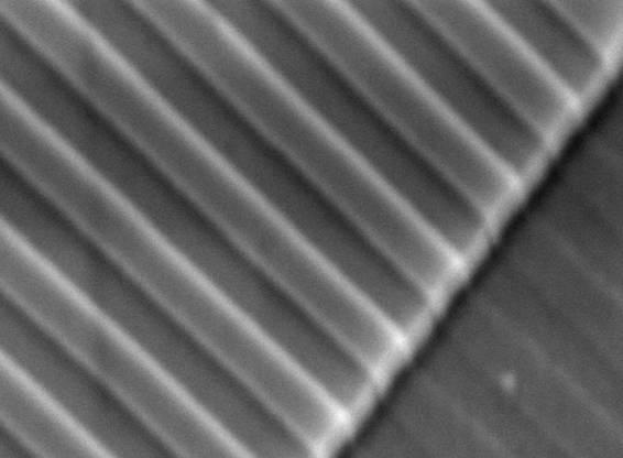
37 Outline Submicron SOI-wires Introduction: why do we need them Basic properties: design, loss, wavelength, polarization Fabrication Devices: couplers, crossings, filters III-V on Silicon Introduction Coupling of light Fabrication PICMOS (Photonic Interconnect on CMOS) 37
38 Fabrication: Review Group loss [db/c m] BOX [um] top clad Fab. Mask Etch Method IMEC no DUV Resist Cl2/He/Hbr/O2 IBM no EBeam SiO 2 CF4/CHF3/Ar (Oxide) + HBr (Silicon) Cornell no EBeam ICP NTT no EBeam SF6/CF4 etch, ECR-etch Yokohama no EBeam metal ICP (CF4 + Xe) MIT yes G-line SiO 2 oxidation RIE (SF6) LETI yes DUV SiO 2 HBr etching 5.0 mixed Columbia yes EBeam Aluminium RIE (CF4:Ar) 38
39 Fabrication EBeam Best suited for research, Features < 50nm Slow, not compatible with mass-fabrication (?) Standard Litho (G-line, I-Line) OK for 500nm lines Problem for smaller features (gaps in direction coupler, PhC, taper tips DUV (248nm, 193nm) Resolution OK (but characterisation needed!) Compatible with Mass-Fabrication Expensive mask 39
40 Original fabrication process AR-coating Si SiO 2 Si-substrate Photoresist Photoresist Bare wafer Photoresist Soft bake AR coating Illumination (UV3) (248nm deep UV) Post bake Development Silicon etch Oxide etch Resist strip 40
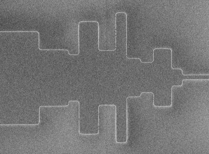
41 Line width with exposure dose 900 Line width (nm) Designed Line Width Exposure dose (mj) 41
42 Hole size with exposure dose Hole size (nm) Marginally sufficient Sufficient Process window Designed Pitch/diameter 400/ / / / / / / / / / / / Exposure dose (mj) 42
43 Process Window Design Pitch/Size: 500nm /300nm Target size: 300nm Focus [µm] Best focus % deviation ellipse λ = 248nm NA = 0.63 resist = UV3 λ = 248nm NA = 0.7 resist = UV3 λ = 248nm NA = 0.7 resist = TIS % -10% -5% Best +5% +10% +15% energy Exposure Energy [ E/E 0 ] λ = 193nm NA = 0.63 resist = TIS 43
44 Process Window Design Pitch/Size: 400nm /240nm Target size: 200nm Focus [µm] Best focus % deviation ellipse λ = 248nm NA = 0.63 resist = UV3 λ = 248nm NA = 0.7 resist = UV3 λ = 248nm NA = 0.7 resist = TIS % -10% -5% Best +5% +10% +15% energy Exposure Energy [ E/E 0 ] λ = 193nm NA = 0.63 resist = TIS 44

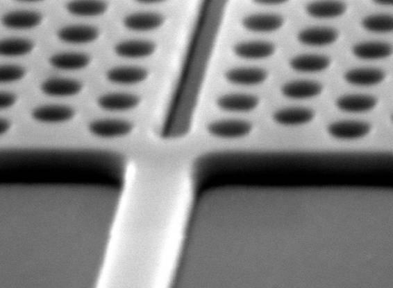
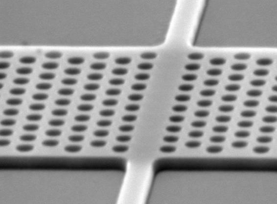
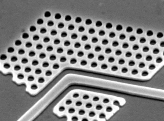
45 Optical proximity effects example: triangular lattice resist pitch = 530nm Diameter = 420nm r/a = 0.4 Bulk hole = 420nm Border hole = 380nm Corner hole = 350nm 1um 45

46 Optical proximity effects W1 waveguide pitch = 500nm hole Ø in bulk lattice = 300nm a/λ Ø border =300nm Light cone Ø border =310nm Ø border =320nm λ(nm) Light cone Light cone Odd lattice modes MSB Odd lattice modes MSB Odd lattice modes MSB Even lattice modes Even lattice modes Even lattice modes k k k 46
 Original Mask layout Resist on wafer Mask layout with OPC http://photonics.intec.ugent.")
47 Optical Proximity Correction Problem: Optical Proximity Effects Holes at lattice boundary are different than holes in bulk due to interference effects Correction on mask required (also on PICCO_03) Original Mask layout Resist on wafer Mask layout with OPC 47
 Border hole Bulk Corner hole Corner hole bias (nm) Border hole bias (nm) http://photonics.intec.ugent.")
48 Optical proximity corrections Determine empirically from PICCO_01 Example: 500nm pitch, nm holes Hole size deviation (nm) Border hole Bulk Corner hole Corner hole bias (nm) Border hole bias (nm) 48
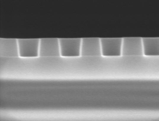
49 Deep Etch Roughness Example: Ring resonator z Straight wire=400nm z Ring wire = 500nm 49


50 Roughness reduction Oxidation Thermal oxidation of top Silicon layer. Lithography Si+SiO 2 Etch 20-60nm thermal oxide optional Oxide removal with HF dip 10nm oxide 30nm oxide 50nm oxide Roughness on air-oxide interface 50


51 Roughness reduction Shallow etching Shallow etching less roughness But: Scattering at bottom of hole Re-fill hole with oxide to reduce asymmetry optional Lithography Si Etch 10nm oxide Oxide deposition 200nm hole 51

52 Silicon-only etch Deep etching Si-only etching Less roughness 52

53 Etch bias with Silicon-only etch Thick resist layer: 800nm UV3 needed for deep etching nm hole Ø: high aspect ratio causes litho-etch bias Litho Etch Result 800nm 300nm hole Ø shadow of thick resist nm hole Ø 53
54 Etch bias with Silicon-only etch Optimal Solution: new litho + etch development: no time. Short-term Solution: Resist-hardening/Resist Trimming plasma treatment Litho RH Etch Result 800nm 300nm hole Ø smaller shadow 300nm hole Ø Still slightly sloped sidewalls 54
55 Updated Fabrication Process AR-coating Si SiO 2 Si-substrate Photoresist Photoresist Bare wafer Photoresist Soft bake AR coating Illumination (UV3) (248nm deep UV) Post bake Development Resist Hardening Silicon etch Resist strip 55
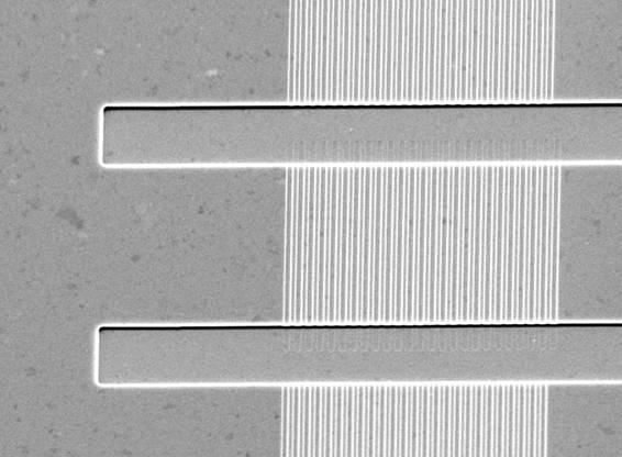
56 2-step processing Two types of structures Waveguides: requires deep etch (al least through Silicon) Fibre couplers: require 50nm etch Two-step processing Fibre couplers first: 50nm etch gives little topography Wafer-scale alignment: Alignment markers on the wafer and reticle periphery, not between the structures 56
57 2-step processing shallow fibre coupler deep trench 57
58 CMOS-compatible? Well, it is Silicon It is processed in a CMOS line But CMOS = layered We: lines, holes, gaps, tips all in same layer CMOS = vias but rather low density Phot Crystals = superdense lattices Line-edge roughness: no issue in CMOS (till now) Roughness kills everything 58
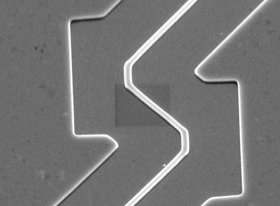
59 Outline Submicron SOI-wires Introduction: why do we need them Basic properties: design, loss, wavelength, polarization Fabrication Devices III-V on Silicon Couplers Introduction Crossings Coupling of light Ring Resonators AWG Fabrication Cascaded MachZehnder PICMOS (Photonic Fibre-chip Interconnect couplers on CMOS) 59
60 Couplers - Splitters Directional Couplers Used in ring resonators, cascaded MZI Easy to choose splitting ratio Sensitive to fabrication issues (optical proximity, deviations in widths) Multi-mode interference couplers (MMI) Fabrication tolerant Standard Y-juncion Symmetric, narrow gap Advanced Couplers Sakai, Fukazawa, Baba, IEICE Trans 02,
 (Sakai, intec Fukazawa, 2004 Baba, IEICE Trans 02, 1033) http://photonics.intec.ugent.")
61 Couplers Yokohama Nat. Univ Simulation: <0.1dB excess loss Experiment: 0.3dB excess loss Some imbalance due to opt. Prox. Other LETI-LPM: 1x8 MMI-coupler (imbalance 0.5dB) (Sakai, intec Fukazawa, 2004 Baba, IEICE Trans 02, 1033) 61
 Large")
 Enhanced versions Better performance Larger NOT acceptable for")
62 Crossings Crosstalk free crossings in optics? Standard crossing Large diffraction Large crosstalk (-9dB) Large loss (1.4dB) Enhanced versions Better performance Larger NOT acceptable for large density circuits Use multiple waveguide layers?? 62


63 Fibre coupling Mode mismatch between waveguide and fibre µm SOI PhC wg InP ridge wg SM-fibre core 63
64 Coupling to fiber Important: Large bandwidth Low loss Fabrication Limited extra processing Tolerant to fabrication deviations Coupling tolerance If coupling to SMF: same for all types of taper Coupling to high-na fiber: lower 64
65 Fiber-chip coupling Regular taper Difficult to fabricate Multi-mode Facet coating required 65
66 Coupling to fiber Inverse taper 0.4µm 0.2µm Broad wavelength range Single mode 500 µm 80nm polished facet Easy to fabricate (if you can do the tips) Low facet reflections 66
67 Coupling to fiber Group h [nm] w [nm] L [um] tip width [nm] Cladding Material Clad ding Size Loss IMEC Polymer tbd IBM Polymer 2x2 < 1dB Cornell SiO2 2x00 < 4dB NTT Polymer 3x µm 0.4µm 500 µm 80nm polishe d facet 67

")

68 Coupling to fibre Tip fabrication EBeam Modified DUV (resist trimming) <100nm 220nm 68
69 Coupling to fiber The vertical fiber coupler use a grating to couple light from/to a fiber perpendicular to the PIC use a spot-size convertor in plane wafer scale, no need to cleave/polish the devices good alignment tolerances relatively broadband works for TE only spot size convertor Single mode fiber core (artist s impression) 69
70 Out-of-plane coupler Grating couplers : Second order grating (Λ=λ /n eff ) First order diffraction couples light out of the waveguide producing a surface normal propagating field What is new? Other grating couplers long (>100µm) very narrow bandwidth couple in and out high efficiency (>50%) Our grating coupler short (10µm) bandwidth > 50nm possible couple in and out high efficiency? 70

![From Fibre Single mode fiber core Transmission [db] -10-15 -20-25 -30 shallow fibre](/docs-images/90/102651639/images/71-2.jpg "coupler deep trench λ 1dB = 35nm Towards optical circuit -35-40 http://photonics.intec.")
71 Fabricated Devices Alternative: Grating couplers Waferscale testing Waferscale packaging High alignment tolerance -5 Wavelength [nm] From Fibre Single mode fiber core Transmission [db] shallow fibre coupler deep trench λ 1dB = 35nm Towards optical circuit
72 bcb cladding, ring resonator with bend coupling, R=8µm T [db] pass drop wavelength [nm] 72

73 Fiber Couplers Coupling light from waveguide to optical fiber on top 73
74 Experimental results 0.40 fiber coupling efficiency nm period 630nm period 620nm theory 630nm theory wavelength (nm) 33% efficiency (4.8dB coupling loss) 35-40nm 1dB bandwidth 74


75 2D grating fiber coupler Fiber to waveguide interface for polarisation independent photonic integrated circuit 2D grating couples each fiber polarisation in its own waveguide in the waveguides the polarisation is the same (TE) Allows for polarisation diversity approach patent Single mode fiber core 75


76 Experimental results Fabrication SOI: 220nm Si / 1000nm SiO 2 Etch depth: 90nm Square lattice of holes: 580nm period 76
 For a given loss: trade-off High Q Low coupling But Low coupling Low drop efficiency!!! http://photonics.intec.ugent.")
77 Optical Ring Resonators Optical Ring Resonators Relevant Characteristics: Free Spectral Range (Period) Quality Factor Determined by: Coupling ratio Round-trip loss Length (=radius) For a given loss: trade-off High Q Low coupling But Low coupling Low drop efficiency!!! 77


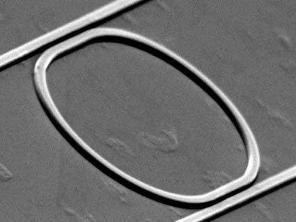
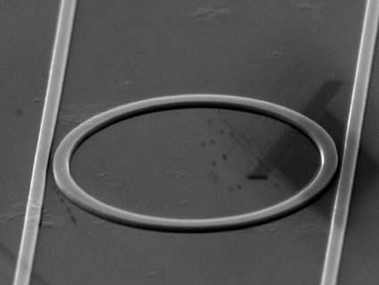
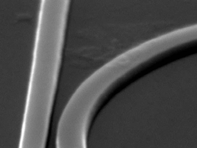
78 Optical Ring Resonator 1um 5um 78
79 Optical Ring Resonators Ring resonator demux 4 rings in series Linearly increasing radius λ c does not increase linearly as expected!! Fabrication problem: mask discretisation Solution: vary parameter which is less sensitive to fabrication Other: Peak splitting due to reflections 79
80 80


 Bend Radius < 50µm")

81 Increasing Index Contrast 5 cm Low Contrast - Fiber Matched (silica or polymer based) Bend Radius ~ 5 mm Size ~ several cm^2 5 mm 200 µm Ulra-high Contrast (SOI based) Bend Radius < 50µm Medium Contrast (InP-InGaAsP) Bend Radius ~ 500µm 81
 different actual waveguide widths http://photonics.intec.ugent.")
82 AWG Design Various devices were designed : R 200µm To grating couplers ν = 400GHz FSR = 8 x 400GHz w g w i w g w w = 0.5µm # arms = 18 or 24 R = 75µm ~ 150µm w i = 0.6µm ~ 1.0µm w g = 0.6µm ~ 1.0µm g = 0.2µm g w i All designs fabricated with different exposure doses (during litho) different actual waveguide widths 82

83 AWG Results 200µm AWG, 400GHz spacing, 8 channels ν = 340GHz 360GHz (different exposure times) 8dB on-chip loss -5 Wavelength [nm] Transmission [db]
84 AWG Results 200µm 5 x 8 AWG, 400GHz spacing, 8 Channels 300µm x 300µm area 8dB on-chip loss 6-10 db crosstalk -5 O2 Wavelength [nm] Transmission [db] dB

")
85 AWG Yokohama Nat. University (Fukazawa, Ohno, Baba, Jap. J of Appl. Physics, 04) 85
86 AWG Crosstalk Origin Possible reasons for crosstalk Overspill in star-coupler Reflections in star-coupler Phase errors in grating arms 86
87 AWG Crosstalk Origin Phase errors in Waveguide arms? Assume standard deviation for phase-error given by : 1 σ φ = π L i i f c Calculated Crosstalk vs. f c f c Crosstalk Level [db] f c =100 Roughness [nm] 10 5 f c =100 f c Correlation length [µm] 87


88 Cascaded MZ Filter Example: 5 stage CMZ 3.2nm bandwidth 17nm FSR coupling efficiency ~80% -10 db crosstalk gap width = 220nm waveguide width = 535nm waveguide width = 565nm normalized output [db] pass drop wavelength [nm] L = 32.8µm 20µm 14µm 20µm 20µm 14µm 20µm 88
89 PICCO04: Cascaded MZ Filter Example: 5 stage CMZ 2.6nm bandwidth 17nm FSR coupling efficiency ~100% gap -10 width db = 220nm crosstalk waveguide width = 535nm waveguide width = 565nm normalized output [db] pass drop wavelength [nm] L = 32.8µm 26µm 14µm 20µm 20µm 14µm 26µm 89
 w i http://photonics.intec.")
90 Optical Proximity Effects Optical Lithography Images of neighbouring structures interfere Effect can be additive of subtractive = optical proximity effects Example: isolated line width: 565 gap width: 220nm w c w g line width in coupling section: 535nm W. Bogaerts et al. to be published in JLT (Oct 2004) w i 90
91 Conclusions Sub-micron SOI-waveguides: Powerful platform for high-density Photonic circuits We have all basic building blocs (and no need for these complicated Photonic Crystals) Fabrication issues to be solved Optical proximity (narrow lines, fine gaps) Phase-Errors, control central wavelength of devices Further reduction losses needed? Next step: active functionality? 91
Figure 1 Basic waveguide structure
 Recent Progress in SOI Nanophotonic Waveguides D. Van Thourhout, P. Dumon, W. Bogaerts, G. Roelkens, D. Taillaert, G. Priem, R. Baets IMEC-Ghent University, Department of Information Technology, St. Pietersnieuwstraat
Integrated photonic circuit in silicon on insulator for Fourier domain optical coherence tomography
 Integrated photonic circuit in silicon on insulator for Fourier domain optical coherence tomography Günay Yurtsever *,a, Pieter Dumon a, Wim Bogaerts a, Roel Baets a a Ghent University IMEC, Photonics
Microphotonics Readiness for Commercial CMOS Manufacturing. Marco Romagnoli
 Microphotonics Readiness for Commercial CMOS Manufacturing Marco Romagnoli MicroPhotonics Consortium meeting MIT, Cambridge October 15 th, 2012 Passive optical structures based on SOI technology Building
Compact wavelength router based on a Silicon-on-insulator arrayed waveguide grating pigtailed to a fiber array
 Compact wavelength router based on a Silicon-on-insulator arrayed waveguide grating pigtailed to a fiber array P. Dumon, W. Bogaerts, D. Van Thourhout, D. Taillaert and R. Baets Photonics Research Group,
Nanophotonic Waveguides and Photonic Crystals in Silicon-on-Insulator
 Nanophotonic Waveguides and Photonic Crystals in Silicon-on-Insulator Wim Bogaerts 19 April 2004 Photonics Research Group http://photonics.intec.ugent.be nano = small photon = elementary on a scale of
Foundry processes for silicon photonics. Pieter Dumon 7 April 2010 ECIO
 Foundry processes for silicon photonics Pieter Dumon 7 April 2010 ECIO Photonics Research Group http://photonics.intec.ugent.be epixfab Prototyping Training Multi project wafer access to silicon photonic
A thin foil optical strain gage based on silicon-on-insulator microresonators
 A thin foil optical strain gage based on silicon-on-insulator microresonators D. Taillaert* a, W. Van Paepegem b, J. Vlekken c, R. Baets a a Photonics research group, Ghent University - INTEC, St-Pietersnieuwstraat
Optics Communications
 Optics Communications 283 (2010) 3678 3682 Contents lists available at ScienceDirect Optics Communications journal homepage: www.elsevier.com/locate/optcom Ultra-low-loss inverted taper coupler for silicon-on-insulator
CHAPTER 2 POLARIZATION SPLITTER- ROTATOR BASED ON A DOUBLE- ETCHED DIRECTIONAL COUPLER
 CHAPTER 2 POLARIZATION SPLITTER- ROTATOR BASED ON A DOUBLE- ETCHED DIRECTIONAL COUPLER As we discussed in chapter 1, silicon photonics has received much attention in the last decade. The main reason is
INTEGRATION of a multitude of photonic functions onto
 JOURNAL OF LIGHTWAVE TECHNOLOGY, VOL. 23, NO. 1, JANUARY 2005 401 Nanophotonic Waveguides in Silicon-on-Insulator Fabricated With CMOS Technology Wim Bogaerts, Member, IEEE, Member, OSA, Roel Baets, Senior
Index. Cambridge University Press Silicon Photonics Design Lukas Chrostowski and Michael Hochberg. Index.
 absorption, 69 active tuning, 234 alignment, 394 396 apodization, 164 applications, 7 automated optical probe station, 389 397 avalanche detector, 268 back reflection, 164 band structures, 30 bandwidth
Lecture: Integration of silicon photonics with electronics. Prepared by Jean-Marc FEDELI CEA-LETI
 Lecture: Integration of silicon photonics with electronics Prepared by Jean-Marc FEDELI CEA-LETI Context The goal is to give optical functionalities to electronics integrated circuit (EIC) The objectives
Silicon Photonics: A Platform for Integration, Wafer Level Assembly and Packaging
 Silicon Photonics: A Platform for Integration, Wafer Level Assembly and Packaging M. Asghari Kotura Inc April 27 Contents: Who is Kotura Choice of waveguide technology Challenges and merits of Si photonics
Design Rules for Silicon Photonics Prototyping
 Design Rules for licon Photonics Prototyping Version 1 (released February 2008) Introduction IME s Photonics Prototyping Service offers 248nm lithography based fabrication technology for passive licon-on-insulator
Section 2: Lithography. Jaeger Chapter 2 Litho Reader. EE143 Ali Javey Slide 5-1
 Section 2: Lithography Jaeger Chapter 2 Litho Reader EE143 Ali Javey Slide 5-1 The lithographic process EE143 Ali Javey Slide 5-2 Photolithographic Process (a) (b) (c) (d) (e) (f) (g) Substrate covered
Comparison between strip and rib SOI microwaveguides for intra-chip light distribution
 Optical Materials 27 (2005) 756 762 www.elsevier.com/locate/optmat Comparison between strip and rib SOI microwaveguides for intra-chip light distribution L. Vivien a, *, F. Grillot a, E. Cassan a, D. Pascal
Section 2: Lithography. Jaeger Chapter 2 Litho Reader. The lithographic process
 Section 2: Lithography Jaeger Chapter 2 Litho Reader The lithographic process Photolithographic Process (a) (b) (c) (d) (e) (f) (g) Substrate covered with silicon dioxide barrier layer Positive photoresist
Silicon Photonics Technology Platform To Advance The Development Of Optical Interconnects
 Silicon Photonics Technology Platform To Advance The Development Of Optical Interconnects By Mieke Van Bavel, science editor, imec, Belgium; Joris Van Campenhout, imec, Belgium; Wim Bogaerts, imec s associated
Silicon-on-insulator nanophotonics
 Silicon-on-insulator nanophotonics Wim Bogaerts a, Pieter Dumon a, Patrick Jaenen b, Johan Wouters b, Stephan Beckx b, Vincent Wiaux b, Dries Van Thourhout a, Dirk Taillaert a, Bert Luyssaert a and Roel
Acknowledgements. Outline. Outline. III-V Silicon heterogeneous integration for integrated transmitters and receivers. Sources Detectors Bonding
 Acknowledgements III-V licon heterogeneous integration for integrated transmitters and receivers Dries Van Thourhout, J. Van Campenhout*, G. Roelkens, J. Brouckaert, R. Baets Ghent University / IMEC, Belgium
Photonic Integrated Circuits Made in Berlin
 Fraunhofer Heinrich Hertz Institute Photonic Integrated Circuits Made in Berlin Photonic integration Workshop, Columbia University, NYC October 2015 Moritz Baier, Francisco M. Soares, Norbert Grote Fraunhofer
Development of a LFLE Double Pattern Process for TE Mode Photonic Devices. Mycahya Eggleston Advisor: Dr. Stephen Preble
 Development of a LFLE Double Pattern Process for TE Mode Photonic Devices Mycahya Eggleston Advisor: Dr. Stephen Preble 2 Introduction and Motivation Silicon Photonics Geometry, TE vs TM, Double Pattern
Dries Van Thourhout IPRM 08, Paris
 III-V silicon heterogeneous integration ti Dries Van Thourhout IPRM 08, Paris InP/InGaAsP epitaxial layer stack Si WG DVS- BCB SiO 2 200nm III-V silicon heterogeneous integration ti Dries Van Thourhout
Reduction in Sidelobe Level in Ultracompact Arrayed Waveguide Grating Demultiplexer Based on Si Wire Waveguide
 Reduction in Sidelobe Level in Ultracompact Arrayed Waveguide Grating Demultiplexer Based on Si Wire Waveguide Fumiaki OHNO, Kosuke SASAKI, Ayumu MOTEGI and Toshihiko BABA Department of Electrical and
Section 2: Lithography. Jaeger Chapter 2. EE143 Ali Javey Slide 5-1
 Section 2: Lithography Jaeger Chapter 2 EE143 Ali Javey Slide 5-1 The lithographic process EE143 Ali Javey Slide 5-2 Photolithographic Process (a) (b) (c) (d) (e) (f) (g) Substrate covered with silicon
Comparison of AWGs and Echelle Gratings for Wavelength Division Multiplexing on Silicon-on-Insulator
 Comparison of AWGs and Echelle Gratings for Wavelength Division Multiplexing on Silicon-on-Insulator Volume 6, Number 5, October 2014 S. Pathak, Member, IEEE P. Dumon, Member, IEEE D. Van Thourhout, Senior
IEEE JOURNAL OF SELECTED TOPICS IN QUANTUM ELECTRONICS 2010 Silicon Photonic Circuits: On-CMOS Integration, Fiber Optical Coupling, and Packaging
 IEEE JOURNAL OF SELECTED TOPICS IN QUANTUM ELECTRONICS 2010 Silicon Photonic Circuits: On-CMOS Integration, Fiber Optical Coupling, and Packaging Christophe Kopp, St ephane Bernab e, Badhise Ben Bakir,
Loss Reduction in Silicon Nanophotonic Waveguide Micro-bends Through Etch Profile Improvement
 Loss Reduction in Silicon Nanophotonic Waveguide Micro-bends Through Etch Profile Improvement Shankar Kumar Selvaraja, Wim Bogaerts, Dries Van Thourhout Photonic research group, Department of Information
Silicon-On-Insulator based guided wave optical clock distribution
 Silicon-On-Insulator based guided wave optical clock distribution K. E. Moselund, P. Dainesi, and A. M. Ionescu Electronics Laboratory Swiss Federal Institute of Technology People and funding EPFL Project
Miniature Mid-Infrared Thermooptic Switch with Photonic Crystal Waveguide Based Silicon-on-Sapphire Mach Zehnder Interferometers
 Miniature Mid-Infrared Thermooptic Switch with Photonic Crystal Waveguide Based Silicon-on- Mach Zehnder Interferometers Yi Zou, 1,* Swapnajit Chakravarty, 2,* Chi-Jui Chung, 1 1, 2, * and Ray T. Chen
Reduction in Sidelobe Level in Ultracompact Arrayed Waveguide Grating Demultiplexer Based on Si Wire Waveguide
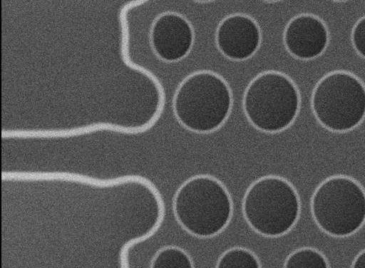
 Japanese Journal of Applied Physics Vol. 45, No. 8A, 26, pp. 6126 6131 #26 The Japan Society of Applied Physics Photonic Crystals and Related Photonic Nanostructures Reduction in Sidelobe Level in Ultracompact
Silicon photonics on 3 and 12 μm thick SOI for optical interconnects Timo Aalto VTT Technical Research Centre of Finland
 Silicon photonics on 3 and 12 μm thick SOI for optical interconnects Timo Aalto VTT Technical Research Centre of Finland 5th International Symposium for Optical Interconnect in Data Centres in ECOC, Gothenburg,
Si-EPIC Workshop: Silicon Nanophotonics Fabrication Fibre Grating Couplers
 Si-EPIC Workshop: Silicon Nanophotonics Fabrication Fibre Grating Couplers June 30, 2012 Dr. Lukas Chrostowski Outline Coupling light to chips using Fibre Grating Couplers (FGC, or GC). Grating coupler
NEXT GENERATION SILICON PHOTONICS FOR COMPUTING AND COMMUNICATION PHILIPPE ABSIL
 NEXT GENERATION SILICON PHOTONICS FOR COMPUTING AND COMMUNICATION PHILIPPE ABSIL OUTLINE Introduction Platform Overview Device Library Overview What s Next? Conclusion OUTLINE Introduction Platform Overview
Silicon photonics with low loss and small polarization dependency. Timo Aalto VTT Technical Research Centre of Finland
 Silicon photonics with low loss and small polarization dependency Timo Aalto VTT Technical Research Centre of Finland EPIC workshop in Tokyo, 9 th November 2017 VTT Technical Research Center of Finland
Linear and Nonlinear Nanophotonic Devices Based on Silicon-on-Insulator Wire Waveguides
 Japanese Journal of Applied Physics Vol. 45, No. 8B, 2006, pp. 6589 6602 #2006 The Japan Society of Applied Physics Review Paper Linear and Nonlinear Nanophotonic Devices Based on Silicon-on-Insulator
Si and InP Integration in the HELIOS project
 Si and InP Integration in the HELIOS project J.M. Fedeli CEA-LETI, Grenoble ( France) ECOC 2009 1 Basic information about HELIOS HELIOS photonics ELectronics functional Integration on CMOS www.helios-project.eu
Characterization of Photonic Structures with CST Microwave Studio. CST UGM 2010 Darmstadt
 Characterization of Photonic Structures with CST Microwave Studio Stefan Prorok, Jan Hendrik Wülbern, Jan Hampe, Hooi Sing Lee, Alexander Petrov and Manfred Eich, Institute of Optical and Electronic Materials
Heinrich-Hertz-Institut Berlin
 NOVEMBER 24-26, ECOLE POLYTECHNIQUE, PALAISEAU OPTICAL COUPLING OF SOI WAVEGUIDES AND III-V PHOTODETECTORS Ludwig Moerl Heinrich-Hertz-Institut Berlin Photonic Components Dept. Institute for Telecommunications,,
Heterogenous integration of InP/InGaAsP photodetectors onto ultracompact Silicon-on-Insulator waveguide circuits
 Heterogenous integration of InP/InGaAsP photodetectors onto ultracompact Silicon-on-Insulator waveguide circuits Günther Roelkens, Joost Brouckaert, Dirk Taillaert, Pieter Dumon, Wim Bogaerts, Richard
Waveguide Bragg Gratings and Resonators LUMERICAL SOLUTIONS INC
 Waveguide Bragg Gratings and Resonators JUNE 2016 1 Outline Introduction Waveguide Bragg gratings Background Simulation challenges and solutions Photolithography simulation Initial design with FDTD Band
SILICON-ON-INSULATOR (SOI) is emerging as an interesting
 is emerging as an interesting") 612 JOURNAL OF LIGHTWAVE TECHNOLOGY, VOL. 27, NO. 5, MARCH 1, 2009 Focusing Polarization Diversity Grating Couplers in Silicon-on-Insulator Frederik Van Laere, Student Member, IEEE, Wim Bogaerts, Member,
612 JOURNAL OF LIGHTWAVE TECHNOLOGY, VOL. 27, NO. 5, MARCH 1, 2009 Focusing Polarization Diversity Grating Couplers in Silicon-on-Insulator Frederik Van Laere, Student Member, IEEE, Wim Bogaerts, Member,
Numerical Analysis and Optimization of a Multi-Mode Interference Polarization Beam Splitter
 Numerical Analysis and Optimization of a Multi-Mode Interference Polarization Beam Splitter Y. D Mello*, J. Skoric, M. Hui, E. Elfiky, D. Patel, D. Plant Department of Electrical Engineering, McGill University,
Holographic Bragg Reflectors: Designs and Applications
 OTuP1.pdf 2009 OSA/OFC/NFOEC 2009 Holographic Bragg Reflectors: Designs and Applications T. W. Mossberg, C. Greiner, D. Iazikov LightSmyth Technologies OFC 2009 Review - Volume Holograms (mode-selective
Near/Mid-Infrared Heterogeneous Si Photonics
 PHOTONICS RESEARCH GROUP Near/Mid-Infrared Heterogeneous Si Photonics Zhechao Wang, PhD Photonics Research Group Ghent University / imec, Belgium ICSI-9, Montreal PHOTONICS RESEARCH GROUP 1 Outline Ge-on-Si
Horizontal single and multiple slot waveguides: optical transmission at λ = 1550 nm
 Horizontal single and multiple slot waveguides: optical transmission at λ = 1550 nm Rong Sun 1 *, Po Dong 2 *, Ning-ning Feng 1, Ching-yin Hong 1, Jurgen Michel 1, Michal Lipson 2, Lionel Kimerling 1 1Department
Compact two-mode (de)multiplexer based on symmetric Y-junction and Multimode interference waveguides
multiplexer based on symmetric Y-junction and Multimode interference waveguides") Compact two-mode (de)multiplexer based on symmetric Y-junction and Multimode interference waveguides Yaming Li, Chong Li, Chuanbo Li, Buwen Cheng, * and Chunlai Xue State Key Laboratory on Integrated Optoelectronics,
Compact two-mode (de)multiplexer based on symmetric Y-junction and Multimode interference waveguides Yaming Li, Chong Li, Chuanbo Li, Buwen Cheng, * and Chunlai Xue State Key Laboratory on Integrated Optoelectronics,
Grating coupled photonic crystal demultiplexer with integrated detectors on InPmembrane
 Grating coupled photonic crystal demultiplexer with integrated detectors on InPmembrane F. Van Laere, D. Van Thourhout and R. Baets Department of Information Technology-INTEC Ghent University-IMEC Ghent,
Realization of Polarization-Insensitive Optical Polymer Waveguide Devices
 644 Realization of Polarization-Insensitive Optical Polymer Waveguide Devices Kin Seng Chiang,* Sin Yip Cheng, Hau Ping Chan, Qing Liu, Kar Pong Lor, and Chi Kin Chow Department of Electronic Engineering,
Fully-Etched Grating Coupler with Low Back Reflection
 Fully-Etched Grating Coupler with Low Back Reflection Yun Wang a, Wei Shi b, Xu Wang a, Jonas Flueckiger a, Han Yun a, Nicolas A. F. Jaeger a, and Lukas Chrostowski a a The University of British Columbia,
High-efficiency fiber-to-chip grating couplers realized using an advanced CMOS-compatible Silicon-On-Insulator platform
 High-efficiency fiber-to-chip grating couplers realized using an advanced CMOS-compatible Silicon-On-Insulator platform D. Vermeulen, 1, S. Selvaraja, 1 P. Verheyen, 2 G. Lepage, 2 W. Bogaerts, 1 P. Absil,
Optomechanical coupling in photonic crystal supported nanomechanical waveguides
 Optomechanical coupling in photonic crystal supported nanomechanical waveguides W.H.P. Pernice 1, Mo Li 1 and Hong X. Tang 1,* 1 Departments of Electrical Engineering, Yale University, New Haven, CT 06511,
New Waveguide Fabrication Techniques for Next-generation PLCs
 New Waveguide Fabrication Techniques for Next-generation PLCs Masaki Kohtoku, Toshimi Kominato, Yusuke Nasu, and Tomohiro Shibata Abstract New waveguide fabrication techniques will be needed to make highly
Convergence Challenges of Photonics with Electronics
 Convergence Challenges of Photonics with Electronics Edward Palen, Ph.D., P.E. PalenSolutions - Optoelectronic Packaging Consulting www.palensolutions.com palensolutions@earthlink.net 415-850-8166 October
Introduction Fundamentals of laser Types of lasers Semiconductor lasers
 ECE 5368 Introduction Fundamentals of laser Types of lasers Semiconductor lasers Introduction Fundamentals of laser Types of lasers Semiconductor lasers How many types of lasers? Many many depending on
Hybrid Integration Technology of Silicon Optical Waveguide and Electronic Circuit
 Hybrid Integration Technology of Silicon Optical Waveguide and Electronic Circuit Daisuke Shimura Kyoko Kotani Hiroyuki Takahashi Hideaki Okayama Hiroki Yaegashi Due to the proliferation of broadband services
Plane wave excitation by taper array for optical leaky waveguide antenna
 LETTER IEICE Electronics Express, Vol.15, No.2, 1 6 Plane wave excitation by taper array for optical leaky waveguide antenna Hiroshi Hashiguchi a), Toshihiko Baba, and Hiroyuki Arai Graduate School of
Waveguiding in PMMA photonic crystals
 ROMANIAN JOURNAL OF INFORMATION SCIENCE AND TECHNOLOGY Volume 12, Number 3, 2009, 308 316 Waveguiding in PMMA photonic crystals Daniela DRAGOMAN 1, Adrian DINESCU 2, Raluca MÜLLER2, Cristian KUSKO 2, Alex.
Part 5-1: Lithography
 Part 5-1: Lithography Yao-Joe Yang 1 Pattern Transfer (Patterning) Types of lithography systems: Optical X-ray electron beam writer (non-traditional, no masks) Two-dimensional pattern transfer: limited
A 3.9 ns 8.9 mw 4 4 Silicon Photonic Switch Hybrid-Integrated with CMOS Driver
 A 3.9 ns 8.9 mw 4 4 Silicon Photonic Switch Hybrid-Integrated with CMOS Driver A. Rylyakov, C. Schow, B. Lee, W. Green, J. Van Campenhout, M. Yang, F. Doany, S. Assefa, C. Jahnes, J. Kash, Y. Vlasov IBM
Silicon Carrier-Depletion-Based Mach-Zehnder and Ring Modulators with Different Doping Patterns for Telecommunication and Optical Interconnect
 Silicon Carrier-Depletion-Based Mach-Zehnder and Ring Modulators with Different Doping Patterns for Telecommunication and Optical Interconnect Hui Yu, Marianna Pantouvaki*, Joris Van Campenhout*, Katarzyna
OPTI510R: Photonics. Khanh Kieu College of Optical Sciences, University of Arizona Meinel building R.626
 OPTI510R: Photonics Khanh Kieu College of Optical Sciences, University of Arizona kkieu@optics.arizona.edu Meinel building R.626 Announcements Homework #3 is due today No class Monday, Feb 26 Pre-record
EE143 Fall 2016 Microfabrication Technologies. Lecture 3: Lithography Reading: Jaeger, Chap. 2
 EE143 Fall 2016 Microfabrication Technologies Lecture 3: Lithography Reading: Jaeger, Chap. 2 Prof. Ming C. Wu wu@eecs.berkeley.edu 511 Sutardja Dai Hall (SDH) 1-1 The lithographic process 1-2 1 Photolithographic
On-chip Si-based Bragg cladding waveguide with high index contrast bilayers
 On-chip Si-based Bragg cladding waveguide with high index contrast bilayers Yasha Yi, Shoji Akiyama, Peter Bermel, Xiaoman Duan, and L. C. Kimerling Massachusetts Institute of Technology, 77 Massachusetts
Design and Analysis of Resonant Leaky-mode Broadband Reflectors
 846 PIERS Proceedings, Cambridge, USA, July 6, 8 Design and Analysis of Resonant Leaky-mode Broadband Reflectors M. Shokooh-Saremi and R. Magnusson Department of Electrical and Computer Engineering, University
Photonic Crystal Slot Waveguide Spectrometer for Detection of Methane
 Photonic Crystal Slot Waveguide Spectrometer for Detection of Methane Swapnajit Chakravarty 1, Wei-Cheng Lai 2, Xiaolong (Alan) Wang 1, Che-Yun Lin 2, Ray T. Chen 1,2 1 Omega Optics, 10306 Sausalito Drive,
On-chip interrogation of a silicon-on-insulator microring resonator based ethanol vapor sensor with an arrayed waveguide grating (AWG) spectrometer
 spectrometer") On-chip interrogation of a silicon-on-insulator microring resonator based ethanol vapor sensor with an arrayed waveguide grating (AWG) spectrometer Nebiyu A. Yebo* a, Wim Bogaerts, Zeger Hens b,roel Baets
On-chip interrogation of a silicon-on-insulator microring resonator based ethanol vapor sensor with an arrayed waveguide grating (AWG) spectrometer Nebiyu A. Yebo* a, Wim Bogaerts, Zeger Hens b,roel Baets
Chapter 1 Silicon Photonic Wire Waveguides: Fundamentals and Applications
 Chapter 1 Silicon Photonic Wire Waveguides: Fundamentals and Applications Koji Yamada Abstract This chapter reviews the fundamental characteristics and basic applications of the silicon photonic wire waveguide.
Development of Vertical Spot Size Converter (SSC) with Low Coupling Loss Using 2.5%Δ Silica-Based Planar Lightwave Circuit
 with Low Coupling Loss Using 2.5%Δ Silica-Based Planar Lightwave Circuit") Development of Vertical Spot Size Converter (SSC) with Low Coupling Loss Using 2.5%Δ Silica-Based Planar Lightwave Circuit Yasuyoshi Uchida *, Hiroshi Kawashima *, and Kazutaka Nara * Recently, new planar
Development of Vertical Spot Size Converter (SSC) with Low Coupling Loss Using 2.5%Δ Silica-Based Planar Lightwave Circuit Yasuyoshi Uchida *, Hiroshi Kawashima *, and Kazutaka Nara * Recently, new planar
Lecture 7. Lithography and Pattern Transfer. Reading: Chapter 7
 Lecture 7 Lithography and Pattern Transfer Reading: Chapter 7 Used for Pattern transfer into oxides, metals, semiconductors. 3 types of Photoresists (PR): Lithography and Photoresists 1.) Positive: PR
A tunable Si CMOS photonic multiplexer/de-multiplexer
 A tunable Si CMOS photonic multiplexer/de-multiplexer OPTICS EXPRESS Published : 25 Feb 2010 MinJae Jung M.I.C.S Content 1. Introduction 2. CMOS photonic 1x4 Si ring multiplexer Principle of add/drop filter
Silicon photonic devices based on binary blazed gratings
 Silicon photonic devices based on binary blazed gratings Zhiping Zhou Li Yu Optical Engineering 52(9), 091708 (September 2013) Silicon photonic devices based on binary blazed gratings Zhiping Zhou Li Yu
CHIRPED FIBER BRAGG GRATING (CFBG) BY ETCHING TECHNIQUE FOR SIMULTANEOUS TEMPERATURE AND REFRACTIVE INDEX SENSING
 BY ETCHING TECHNIQUE FOR SIMULTANEOUS TEMPERATURE AND REFRACTIVE INDEX SENSING") CHIRPED FIBER BRAGG GRATING (CFBG) BY ETCHING TECHNIQUE FOR SIMULTANEOUS TEMPERATURE AND REFRACTIVE INDEX SENSING Siti Aisyah bt. Ibrahim and Chong Wu Yi Photonics Research Center Department of Physics,
CHIRPED FIBER BRAGG GRATING (CFBG) BY ETCHING TECHNIQUE FOR SIMULTANEOUS TEMPERATURE AND REFRACTIVE INDEX SENSING Siti Aisyah bt. Ibrahim and Chong Wu Yi Photonics Research Center Department of Physics,
Examination Optoelectronic Communication Technology. April 11, Name: Student ID number: OCT1 1: OCT 2: OCT 3: OCT 4: Total: Grade:
 Examination Optoelectronic Communication Technology April, 26 Name: Student ID number: OCT : OCT 2: OCT 3: OCT 4: Total: Grade: Declaration of Consent I hereby agree to have my exam results published on
This writeup is adapted from Fall 2002, final project report for by Robert Winsor.
 Optical Waveguides in Andreas G. Andreou This writeup is adapted from Fall 2002, final project report for 520.773 by Robert Winsor. September, 2003 ABSTRACT This lab course is intended to give students
Silicon Photonics Opportunity, Applicatoins & Recent Results. Mario Paniccia, Director Photonics Technology Lab Intel Corporation
 Silicon Photonics Opportunity, Applicatoins & Recent Results Mario Paniccia, Director Photonics Technology Lab Intel Corporation Intel Corporation CREOL April 1 2005 Agenda Opportunity for Silicon Photonics
Optical Amplifiers Photonics and Integrated Optics (ELEC-E3240) Zhipei Sun Photonics Group Department of Micro- and Nanosciences Aalto University
 Zhipei Sun Photonics Group Department of Micro- and Nanosciences Aalto University") Photonics Group Department of Micro- and Nanosciences Aalto University Optical Amplifiers Photonics and Integrated Optics (ELEC-E3240) Zhipei Sun Last Lecture Topics Course introduction Ray optics & optical
Photonics Group Department of Micro- and Nanosciences Aalto University Optical Amplifiers Photonics and Integrated Optics (ELEC-E3240) Zhipei Sun Last Lecture Topics Course introduction Ray optics & optical
Photolithography I ( Part 1 )
") 1 Photolithography I ( Part 1 ) Chapter 13 : Semiconductor Manufacturing Technology by M. Quirk & J. Serda Bjørn-Ove Fimland, Department of Electronics and Telecommunication, Norwegian University of Science
1 Photolithography I ( Part 1 ) Chapter 13 : Semiconductor Manufacturing Technology by M. Quirk & J. Serda Bjørn-Ove Fimland, Department of Electronics and Telecommunication, Norwegian University of Science
Demonstration of Silicon-on-insulator midinfrared spectrometers operating at 3.8μm
 Demonstration of Silicon-on-insulator midinfrared spectrometers operating at 3.8μm M. Muneeb, 1,2,3,* X. Chen, 4 P. Verheyen, 5 G. Lepage, 5 S. Pathak, 1 E. Ryckeboer, 1,2 A. Malik, 1,2 B. Kuyken, 1,2
Lithography. 3 rd. lecture: introduction. Prof. Yosi Shacham-Diamand. Fall 2004
 Lithography 3 rd lecture: introduction Prof. Yosi Shacham-Diamand Fall 2004 1 List of content Fundamental principles Characteristics parameters Exposure systems 2 Fundamental principles Aerial Image Exposure
Introduction and concepts Types of devices
 ECE 6323 Introduction and concepts Types of devices Passive splitters, combiners, couplers Wavelength-based devices for DWDM Modulator/demodulator (amplitude and phase), compensator (dispersion) Others:
Low Loss Ultra-Small Branches in a Silicon Photonic Wire Waveguide
 IEICE TRANS. ELECTRON., VOL.E85 C, NO.4 APRIL 22 133 PAPER Special Issue on Recent Progress of Integrated Photonic Devices Low Loss Ultra-Small Branches in a Silicon Photonic Wire Waveguide Atsushi SAKAI,
Contents Silicon Photonic Wire Waveguides: Fundamentals and Applications
 1 Silicon Photonic Wire Waveguides: Fundamentals and Applications.. 1 Koji Yamada 1.1 Introduction... 1 1.2 Fundamental Design of Silicon Photonic Wire Waveguides... 3 1.2.1 Guided Modes... 3 1.2.2 Effect
 Chapter 5 5.1 What are the factors that determine the thickness of a polystyrene waveguide formed by spinning a solution of dissolved polystyrene onto a substrate? density of polymer concentration of polymer
Semiconductor Optical Communication Components and Devices Lecture 18: Introduction to Diode Lasers - I
 Semiconductor Optical Communication Components and Devices Lecture 18: Introduction to Diode Lasers - I Prof. Utpal Das Professor, Department of lectrical ngineering, Laser Technology Program, Indian Institute
Photonics and Optical Communication
 Photonics and Optical Communication (Course Number 300352) Spring 2007 Dr. Dietmar Knipp Assistant Professor of Electrical Engineering http://www.faculty.iu-bremen.de/dknipp/ 1 Photonics and Optical Communication
SUPPLEMENTARY INFORMATION
 SUPPLEMENTARY INFORMATION doi:0.038/nature727 Table of Contents S. Power and Phase Management in the Nanophotonic Phased Array 3 S.2 Nanoantenna Design 6 S.3 Synthesis of Large-Scale Nanophotonic Phased
Winter College on Optics: Fundamentals of Photonics - Theory, Devices and Applications February 2014
 2572-10 Winter College on Optics: Fundamentals of Photonics - Theory, Devices and Applications 10-21 February 2014 Photonic packaging and integration technologies II Sonia M. García Blanco University of
Design, Simulation & Optimization of 2D Photonic Crystal Power Splitter
 Optics and Photonics Journal, 2013, 3, 13-19 http://dx.doi.org/10.4236/opj.2013.32a002 Published Online June 2013 (http://www.scirp.org/journal/opj) Design, Simulation & Optimization of 2D Photonic Crystal
SUPPLEMENTARY INFORMATION
 Supplementary Information "Large-scale integration of wavelength-addressable all-optical memories in a photonic crystal chip" SUPPLEMENTARY INFORMATION Eiichi Kuramochi*, Kengo Nozaki, Akihiko Shinya,
UC Santa Barbara UC Santa Barbara Previously Published Works
 UC Santa Barbara UC Santa Barbara Previously Published Works Title Compact broadband polarizer based on shallowly-etched silicon-on-insulator ridge optical waveguides Permalink https://escholarship.org/uc/item/959523wq
Impact of the light coupling on the sensing properties of photonic crystal cavity modes Kumar Saurav* a,b, Nicolas Le Thomas a,b,
 Impact of the light coupling on the sensing properties of photonic crystal cavity modes Kumar Saurav* a,b, Nicolas Le Thomas a,b, a Photonics Research Group, Ghent University-imec, Technologiepark-Zwijnaarde
Cost-effective CMOS-compatible grating couplers with backside metal mirror and 69% coupling efficiency
 Cost-effective CMOS-compatible grating couplers with backside metal mirror and 69% coupling efficiency Wissem Sfar Zaoui, 1,* María Félix Rosa, 1 Wolfgang Vogel, 1 Manfred Berroth, 1 Jörg Butschke, 2 and
FABRICATION OF CMOS INTEGRATED CIRCUITS. Dr. Mohammed M. Farag
 FABRICATION OF CMOS INTEGRATED CIRCUITS Dr. Mohammed M. Farag Outline Overview of CMOS Fabrication Processes The CMOS Fabrication Process Flow Design Rules Reference: Uyemura, John P. "Introduction to
Ultracompact Adiabatic Bi-sectional Tapered Coupler for the Si/III-V Heterogeneous Integration
 Ultracompact Adiabatic Bi-sectional Tapered Coupler for the Si/III-V Heterogeneous Integration Qiangsheng Huang, Jianxin Cheng 2, Liu Liu, 2, 2, 3,*, and Sailing He State Key Laboratory for Modern Optical
WAVELENGTH division multiplexing (WDM) is now
 is now") Optimized Silicon AWG With Flattened Spectral Response Using an MMI Aperture Shibnath Pathak, Student Member, IEEE, Michael Vanslembrouck, Pieter Dumon, Member, IEEE, Dries Van Thourhout, Member, IEEE,
Optimized Silicon AWG With Flattened Spectral Response Using an MMI Aperture Shibnath Pathak, Student Member, IEEE, Michael Vanslembrouck, Pieter Dumon, Member, IEEE, Dries Van Thourhout, Member, IEEE,
2D silicon-based surface-normal vertical cavity photonic crystal waveguide array for high-density optical interconnects
 2D silicon-based surface-normal vertical cavity photonic crystal waveguide array for high-density optical interconnects JaeHyun Ahn a, Harish Subbaraman b, Liang Zhu a, Swapnajit Chakravarty b, Emanuel
Silicon Photonics Opportunity, applications & Recent Results
 Silicon Photonics Opportunity, applications & Recent Results Dr. Mario Paniccia Intel Fellow Director, Photonics Technology Lab Intel Corporation www.intel.com/go/sp Purdue University Oct 5 2007 Agenda
Lecture 6 Fiber Optical Communication Lecture 6, Slide 1
 Lecture 6 Optical transmitters Photon processes in light matter interaction Lasers Lasing conditions The rate equations CW operation Modulation response Noise Light emitting diodes (LED) Power Modulation
Spontaneous Hyper Emission: Title of Talk
 Spontaneous Hyper Emission: Title of Talk Enhanced Light Emission by Optical Antennas Ming C. Wu University of California, Berkeley A Science & Technology Center Where Our Paths Crossed Page Nanopatch