Si-EPIC Workshop: Silicon Nanophotonics Fabrication Fibre Grating Couplers
|
|
|
- Laureen Bridges
- 6 years ago
- Views:
Transcription

1 Si-EPIC Workshop: Silicon Nanophotonics Fabrication Fibre Grating Couplers June 30, 2012 Dr. Lukas Chrostowski
2 Outline Coupling light to chips using Fibre Grating Couplers (FGC, or GC). Grating coupler physics Tutorial on modelling 2
![lower than -40 db [5] that is ignored in our simulation. calculated as functions of the coupling coe cients. The waveguide effective indices are calculated by a 2D finite-difference mode solver [9].](/docs-images/77/76613711/images/3-1.jpg "The coupling coe cients of the directional couplers using coupled390 Caryare Gunncalculated and Thomas L. Koch Fiber input Fiber output mode theory [10].")
![w Coupling coe cients are critical to the performance of microring resonators [2] and, as shown in Fig. 2, signifisi SiO magnitude, cladding cantlyl affect the shape, Q factor, and extinc2!](/docs-images/77/76613711/images/3-2.jpg "m Input port tion ratio of the reflection spectrum.")
, where Rp is the Si substrate")
![maximum reflectivity and Rv is[28]. Reflection port Figure 11.7 typically Schematic of waveguide 10x10 with nano-taper coupler umthe minimum reflectivity. Based on the results shown in Fig.](/docs-images/77/76613711/images/3-4.jpg "3, we choose 12 Heat sink photonics [31, 32] have a number of unique traits a relatively small number of to be 0.84 and to be 0.")


![Measurement schematic with an inset showing optical mode with lateral dimensions equivalent to the core of an optical fiber, or shown in Fig. 4. Periodic grating couplers [11] are used to!](/docs-images/77/76613711/images/3-8.jpg "10 mm in length. An example of a grating coupler is shown in Figure 11.8. an image of the Y-branch power splitter. couple light into and out of the waveguides. A Y-branch www.download-it.")
3 lower than -40 db [5] that is ignored in our simulation. calculated as functions of the coupling coe cients. The waveguide effective indices are calculated by a 2D finite-difference mode solver [9]. The coupling coe cients of the directional couplers using coupled390 Caryare Gunncalculated and Thomas L. Koch Fiber input Fiber output mode theory [10]. w Coupling coe cients are critical to the performance of microring resonators [2] and, as shown in Fig. 2, signifisi SiO magnitude, cladding cantlyl affect the shape, Q factor, and extinc2!m Input port tion ratio of the reflection spectrum. Therefore, we use h Are used to couple light in/out of the chip a racetrack shape to carefully control the coupling coefw via the top Buried SiO coupling condition, we scan ficients. To find the optimal Through port the reflection spectrum as a function of 12 and 34 and Input coupler similar electrical pads calculate Rp Rvtoand 10log(Rp /R v ), where Rp is the Si substrate maximum reflectivity and Rv is[28]. Reflection port Figure 11.7 typically Schematic of waveguide 10x10 with nano-taper coupler umthe minimum reflectivity. Based on the results shown in Fig. 3, we choose 12 Heat sink photonics [31, 32] have a number of unique traits a relatively small number of to be 0.84 and to be 0.77 in order to satisfy the dual34 tocan have chip grating teeth, a desire mode-match to the hundreds Gaussian output of a per single-mode Temperature controller fiber, and criteria a remarkably of widehigh optical reflectivity bandwidth. and high extinction ratio. A silicon-grating coupler exploits the high index contrast between silicon and The was fabricated by epixfab at IMEC using silicon dioxide, as welldevice as the sub-wavelength patterning capabilities of a modern DUV lithography process, to create a grating capable of creating a well-controlled schematic is 193 nm photolithography. The measurement Fig. 4. Measurement schematic with an inset showing optical mode with lateral dimensions equivalent to the core of an optical fiber, or shown in Fig. 4. Periodic grating couplers [11] are used to!10 mm in length. An example of a grating coupler is shown in Figure an image of the Y-branch power splitter. couple light into and out of the waveguides. A Y-branch e reference: t9svae7agovn5h9q6o7tp6cpk6-2587, for 1 user on Jun 19, 2010 to Customize Your Account lukasc@gmail.com Grating Couplers w 2 t In pu tl ig ht t 2 etp:// reference: t9svae7agovn5h9q6o7tp6cpk6-2587, for 1 user on Jun 19, 2010 to Customize Your Account lukasc@gmail.com 2 Luxtera Inc. Figure 11.8 Oblique view of a planar grating coupler structure employing curved gratings, nonuniform pitch, and non-uniform periodicity. This particular device is formed using curved polysilicon gratings formed on top of a planar silicon slab which is tapered down to a single mode silicon waveguide. Image courtesy Luxtera, Inc. r 11 Silicon Photonics From Optical Fiber Telecommunications - V Ivan P. Kaminow, Tingye Li and Alan E. Willner 3

4 Grating Fiber Coupler single-mode fibre, 10 adiabatic taper (>150µm) TE to integrated circuit grating 10µm wide waveguide intec 2008 UBC EECE - Photonics 584 / CMC Workshop Research Silicon Group Nanophotonics - Fabrication 4
 31 % efficiency (5.")

5 1-D grating coupler Experimental results (λ=630nm,depth=70nm, TE pol.) 31 % efficiency (5.1 db coupling loss) 40nm 1dB bandwidth Also acts as a broadband filter shallow grating deep trench intec 2008 UBC EECE - Photonics 584 / CMC Workshop Research Silicon Group Nanophotonics - Fabrication 5
 patented TE intec 2008 UBC EECE - Photonics 584 / CMC Workshop Research Silicon Group Nanophotonics - http://photonics.intec.ugent.")
6 2-D grating + polarization splitter 10 Fiber-to-waveguide interface for polarization independent photonic integrated circuit 2-D grating, 2 waveguides couples each fiber polarization in its own waveguide TE in the waveguides the polarization is the same (TE) patented TE intec 2008 UBC EECE - Photonics 584 / CMC Workshop Research Silicon Group Nanophotonics - Fabrication 6
7 single-mode fiber Polarisation Diversity Circuit light in y x on-chip components are polarisation dependent fiber-to-fiber transmission is polarisation independent light out x-polarization 2-D grating split polarisations identical circuits y-polarization z y x combine polarisations patented 2-D grating intec 2008 UBC EECE - Photonics 584 / CMC Workshop Research Silicon Group Nanophotonics - Fabrication 7


?")
8 Measurement!"#$%&'(# )*+,-./#0,1/2#3#4/5/6572# ;G98# ;,E/2,# G=627167>/# (H#0/+1/F# "G#I-/2#!7.F/2#!7.F/2# ;7E>*5/2# G7+=572# 89:#;<=># )/E>/2,5*2/# ; /2# 8
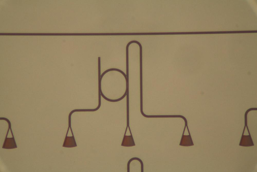
 1220 nm tunable laser Grating Grating 12.5 um 25 um 50 um Grating Grating Grating Grating 4 mm 9")
9 Semi-Automated Optical Probe Station 2 fibres All-band Agilent tunable laser (180 nm span, nm) 1220 nm tunable laser Grating Grating 12.5 um 25 um 50 um Grating Grating Grating Grating 4 mm 9

10 Automated Probe Station Fibre Array 10
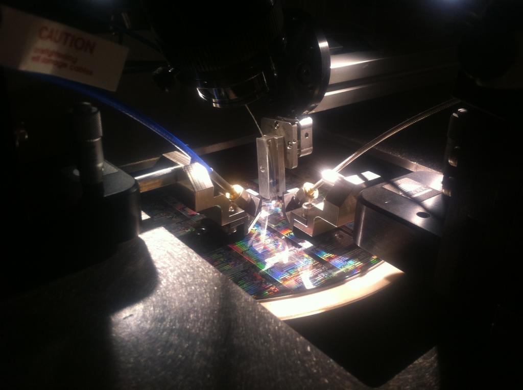
11 11
12 Automated Probe Station Fibre Array 127 µm fibre spacing 2 separate devices 127 µm 127 µm 12
13 13
14 14
15 15
16 16
17 FDTD Tutorial Grating Couplers
18 Grating Coupler Operation Case 1 Optical wavelength inside the grating matches its period, 0 n e = K = 2 = n e k 0 = 2 n e Vertical output (1 st diffraction order), plus back-reflection (from 2 nd diffraction order) 0 18
19 Grating Coupler Operation Detuned Case 2 Optical wavelength is smaller than the grating period, 0 n e < K = 2 = n e k 0 = 2 n e Vertical output at an angle, no 2 nd order back-reflection 0 19
20 Grating Coupler Bragg Condition =sin 1 k x k 0 n 1 =1 y k x = k 0 = 2 0 mk Grating, m=2 = n e k 0 = 2 n e waveguide propagation constant 0 x 2K =2 2 K = 2 n 2 = n SiO2 Grating, m=1 20
21 Gratings Bragg condition Bragg condition Grating s scattering modifies the light s wave-vector to be (in the direction of propagation, x): Slab s effective index in the region of the grating: for 220 nm thick ~ for 150 nm thick ~ k x = mk = m 2 Duty cycle is 50%, thus estimate average effective index to be k x = K = µm µm = = 1.069µm 1 21
22 Gratings Bragg condition We know the free-space wave-vector: k 0 = 2 0 =4.05µm 1 Estimated diffracted angle is: =sin 1 k x k 0 =sin =
23 Detuned second-order gratings: A first generation of gratings was etched 40 to 50nm deep, with a 610 nm pitch and uniform 50% fill factor. These have a coupling efficiency of about 20% and a 60 nm 3 db bandwidth [16] without index matching material between grating and fibre. The second generation of couplers used has a 70 nm etch depth, a 630 nm pitch and a higher coupling efficiency of up to 35% when cladded with oxide, with an almost 60 nm wide 3 db bandwidth. [Pieter Dumon thesis] 23
24 Source: Dirk Taillaert, PhD Thesis, IMEC 24
25 Dirk Taillaert, PhD Thesis, IMEC Vertical coupling Source: Dirk Taillaert, PhD Thesis, IMEC The case of vertical coupling ( =0) is very interesting from a practical point of view. Vertical coupling can be achieved when the grating period equals the wavelength divided by the refractive index. For a very shallow grating, this index is the effective index of the waveguide mode. As mentioned in chapter 3, this grating is called a second order grating. But for the grating coupler, the first order diffraction is used. The second order diffraction is reflecting back into the waveguide. To avoid any confusion, we will use the term coupler grating instead of second order grating in the rest of this work. Figure 4.2 shows the reflection R as a function of wavelength for dif Almost vertical coupling To avoid the reflection at the grating, we have to choose a working point away from the second order reflection peak. Either a shorter or longer wavelength can be chosen. As a result, light is coupled out not exactly vertical, but at a small angle with respect to the vertical direction. This grating is also called a detuned grating. Instead of changing the wavelength, the grating period can be changed. The grating can be negatively or positively detuned (figure 4.5). In a negatively detuned grating, the grating period is smaller (K is larger) or the wavelength is longer ( is smaller) compared to the case of vertical coupling. In a positively detuned grating, the grating period is larger ( is smaller) or 25
26 Source: Dirk Taillaert, PhD Thesis, IMEC power up fibre 10 reflection power up fibre 8 reflection wavelength (nm) (a) with air on top wavelength (nm) (b) with index matching layer Figure 4.8: Calculated coupling efficiency to fibre for an optimized uniform grating and near vertical coupling. =630 nm, ed=70 nm, ff=0.5, N=20, 26
27 Experimental Alignment Tolerances Source: Dirk Taillaert, PhD Thesis, IMEC 4 3 1dB z offset (µm) dB 1dB 0.5dB 0.5dB 1dB 3dB x offset (µm) (b) measurement results Figure 6.9: Experimental alignment tolerances. 27
28 Resources - Grating Couplers Book chapter: David J. Lockwood and Lorenzo Pavesi, Silicon Photonics II Components and Integration, 2011, Online PDF Chapter 3 Interfacing Silicon Nanophotonic Integrated Circuits and Single-Mode Optical Fibers with Diffraction Gratings (IMEC) Chrostowski and Hochberg, Silicon Photonics Design, Ch. Optical I/O Thesis: Dirk Taillaert, PhD Thesis, IMEC Journal papers: Luxtera: A. Mekis et al. A Grating-Coupler-Enabled CMOS Photonics Platform. IEEE Journal of Selected Topics in Quantum Electronics, 17.3 (2011), pp issn: X. doi: /JSTQE
29 Grating Coupler Modelling Approach: 1) Waveguide to air 2D FDTD Start with mode-source in the waveguide, measure output power in free-space far-field, check angle 2) Air to waveguide 2D FDTD Start from optical fibre Gaussian mode incident on grating. Measure power in the waveguide use previous angle, vary position Fibre mode MFD ) optimize for 1550 nm 4) validate design 3D FDTD 29
 Etch 70 nm (150 nm remaining) Oxide index 1.444 Si index: 3.47 constant, vs.")
30 IMEC Coupler Oxide 2 µm Cladding 2 µm check? Silicon 0.22 µm Period 0.63 µm Fill 0.32 µm (each tooth) Etch 70 nm (150 nm remaining) Oxide index Si index: 3.47 constant, vs. Palik data dispersive? 30

31 1) Output Grating Coupler simulation Launch a mode in the slab Monitor the output far-field pattern vs. angle (for a specific wavelength) 31

32 3D FDTD Fibre Grating Coupler object 32
33 Setup 33
")
34 Far field projection Peak angle is between 10-20º (wavelength dependant) 34

35 Total output power 1545 nm peak wavelength Power out 56% 35

![y Position [um] 10 5 0 0 2 4 6](/docs-images/77/76613711/images/36-2.jpg "8 10 12 14 16 x Position [um]")
36 e.g., Grating coupler, 2D FDTD simulation, accuracy=5 y Position [um] x Position [um] 36
 Measure transmission spectrum into slab waveguide Sweeps: angle,")
37 2) Input Grating Coupler simulation Gaussian beam input (waist diameter 10.5 µm) Measure transmission spectrum into slab waveguide Sweeps: angle, position 37
38 Setup 38


39 Setup FDTD 7: FDTD 8: 39


40 Setup Movie Move the movie monitor into simulation region. Setup script is automatically executed before simulation 40


41 Run Run simulation Run analysis script runanalysis; 41
; plot ( lambda, 10*log10(abs(Tspectrum)),\"Wavelength\",\"Power Coupled\", \"Grating coupler efficiency\"); setplot(\"x min\", 1.")
42 Runanalysis; # Transmission at 1550 nm lambda=c/getdata("coupled","f"); Tspectrum=transmission("coupled"); T_1550=interp(Tspectrum,lambda,1550e-9); # Spectrum plot ( lambda, Tspectrum,"Wavelength","Power Coupled", "Grating coupler efficiency"); plot ( lambda, 10*log10(abs(Tspectrum)),"Wavelength","Power Coupled", "Grating coupler efficiency"); setplot("x min", 1.5e-6); setplot("x max", 1.6e-6); setplot("y min", -15); setplot("y max", 0); setplot("y label", "Coupling, db"); Tspectrum1=transmission("below"); plot ( lambda, 10*log10(abs(Tspectrum1)),"Wavelength","Power Coupled", "GC - into substrate"); setplot("x min", 1.5e-6); setplot("x max", 1.6e-6); setplot("y min", min(10*log10(abs(tspectrum1)))-1); setplot("y max", 0); setplot("y label", "db"); Tspectrum1=transmission("above"); plot ( lambda, 10*log10(abs(Tspectrum1)),"Wavelength","Power Coupled", "GC - refection"); setplot("x min", 1.5e-6); setplot("x max", 1.6e-6); setplot("y min", min(10*log10(abs(tspectrum1)))-1); setplot("y max", 0); setplot("y label", "db"); Tspectrum1=transmission("backwards"); plot ( lambda, 10*log10(abs(Tspectrum1)),"Wavelength","Power Coupled", "GC - backwards, waveguide"); setplot("x min", 1.5e-6); setplot("x max", 1.6e-6); setplot("y min", min(10*log10(abs(tspectrum1)))-1); setplot("y max", 0); setplot("y label", "Coupling, db"); # 42
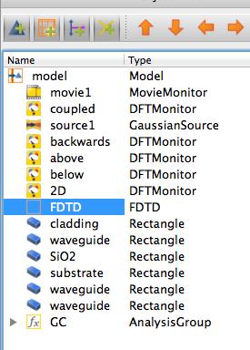
43 Simulation Results 43
44 Where is the coupling loss from? 44

45 Optimization Optimize the gaussian beam angle the position of the beam Done either with optimization or with sweep 45

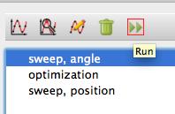
46 Sweep Angle 46
; lambda=c/getdata(\"coupled\",\"f\"); NUM=length(angles); T_data=getsweepdata(\"sweep, angle\",\"tspectrum\"); plot ( lambda, T_data,\"Wavelength\",\"Power Coupled\",")
)+\" to \" +num2str(angles(num))); legend (num2str(angles(1))); setplot(\"x min\", 1.5e-6); setplot(\"x max\", 1.")
47 After it is done, run the script to analyze all the data. # plot the results from an FDTD sweep on position. angles=getsweepdata("sweep, angle","angle"); lambda=c/getdata("coupled","f"); NUM=length(angles); T_data=getsweepdata("sweep, angle","tspectrum"); plot ( lambda, T_data,"Wavelength","Power Coupled", "Gaussian angles: "+num2str(angles(1))+" to " +num2str(angles(num))); legend (num2str(angles(1))); setplot("y label", "Coupling"); plot ( lambda, 10*log10(abs(T_data)),"Wavelength","Power Coupled", "Gaussian angles: "+num2str(angles(1))+" to " +num2str(angles(num))); legend (num2str(angles(1))); setplot("x min", 1.5e-6); setplot("x max", 1.6e-6); setplot("y min", -15); setplot("y max", 0); setplot("y label", "Coupling, db"); T_1550=getsweepdata("sweep, angle","t_1550"); plot ( angles, 10*log10(T_1550), 1550"); setplot("x label", "Angle"); setplot("y label", "Coupling, db"); matlabsave("gc_in_sweep,angle",t_data,angles,lambda); # 47
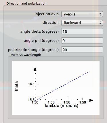
48 Gaussian input Angle Mesh accuracy = 2 (auto mesh, conformal) About 5-10 nm per degree tuning 48

49 Gaussian Input Angle Mesh accuracy = 4 (auto mesh, conformal) 49

50 Sweep Position 50
51 Gaussian Input Position 51

52 Sweep Buried Oxide Thickness Sweep the oxide thickness Achieved by overlapping the oxide on top of the silicon substrate, and changing the y-min of the oxide. 52
53 Oxide thickness 2 µm Oscillations as a function of thickness are a result of constructive/destructive interference from the oxide layer. 53
54 Optimized with 10 nm mesh-x 16º injection angle, optimized laterally: 10 µm peak is nm db coupling efficiency with auto-mesh, accuracy=4 54

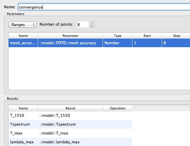
55 Sweep Mesh accuracy Convergence test 55
56 Convergence Test Without Mesh Override 56

57 Convergence Test Using Mesh Override Conclusion: Slightly faster convergence 57
58 Sensitivity to Accuracy Using mesh overrides to ensure correctly-periodic mesh Error is < 10 nm, ~0.01 coupling error 58

59 Manual mesh Mesh override: 10 nm grid in the waveguide & grating 59

60 3D FDTD Grating Coupler 60
61 3D FDTD Grating Coupler Layout imported from GDS FDTD simulation region includes substrate and cladding: -2.4 µm < z < 3.0 µm Gaussian beam input, above the oxide Beam centre offset 5 µm from 1 st grating tooth. Power monitors: in the taper (faster simulation time) in the waveguide (include taper in the simulation, 2X longer) 61

62 GDS Grating coupler IMEC 62
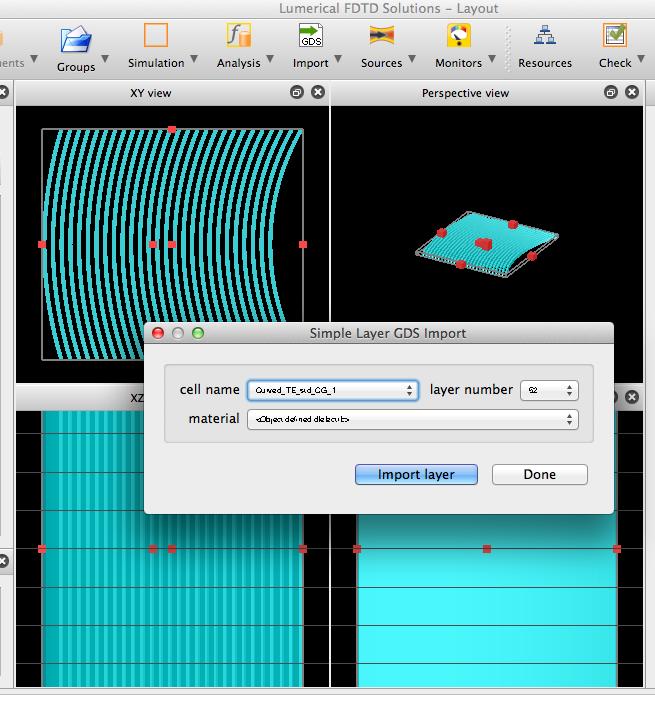
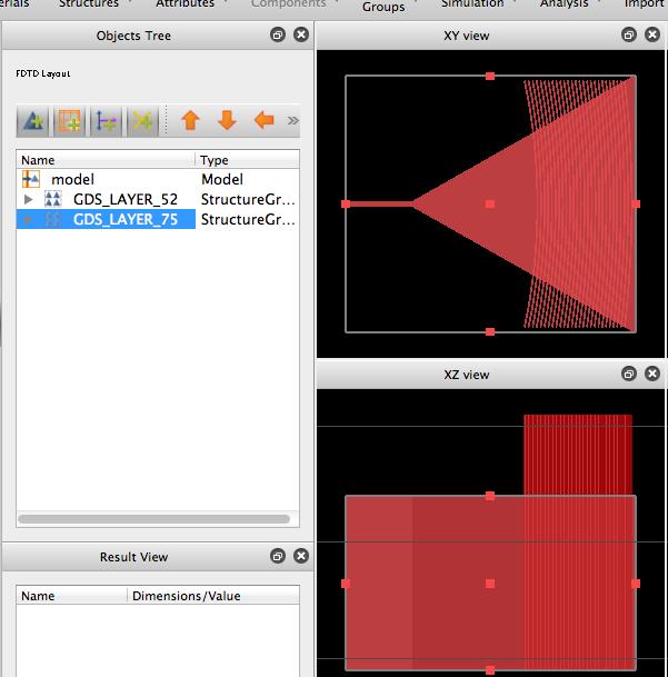
63 GDS Import GDS: TE_Curved_Grating_coupler_right Layer 52, Silicon, edit to be 220 nm Layer 75, Silicon, edit to be 150 nm 63
64 3D FDTD Grating Coupler Mesh accuracy = 1 (several minutes) Mesh accuracy = 2 (several tens minutes) 64
65 3D FDTD Grating Coupler Core i7 ~$1000 linux Accuracy Time hh:mm:ss increasing accuracy 1 00:03: :15: :47: :56: :46: :27:00 65
Si-EPIC Workshop: Silicon Nanophotonics Fabrication Directional Couplers
 Si-EPIC Workshop: Silicon Nanophotonics Fabrication Directional Couplers June 26, 2012 Dr. Lukas Chrostowski Directional Couplers Eigenmode solver approach Objectives Model the power coupling in a directional
Index. Cambridge University Press Silicon Photonics Design Lukas Chrostowski and Michael Hochberg. Index.
 absorption, 69 active tuning, 234 alignment, 394 396 apodization, 164 applications, 7 automated optical probe station, 389 397 avalanche detector, 268 back reflection, 164 band structures, 30 bandwidth
CHAPTER 2 POLARIZATION SPLITTER- ROTATOR BASED ON A DOUBLE- ETCHED DIRECTIONAL COUPLER
 CHAPTER 2 POLARIZATION SPLITTER- ROTATOR BASED ON A DOUBLE- ETCHED DIRECTIONAL COUPLER As we discussed in chapter 1, silicon photonics has received much attention in the last decade. The main reason is
Fully-Etched Grating Coupler with Low Back Reflection
 Fully-Etched Grating Coupler with Low Back Reflection Yun Wang a, Wei Shi b, Xu Wang a, Jonas Flueckiger a, Han Yun a, Nicolas A. F. Jaeger a, and Lukas Chrostowski a a The University of British Columbia,
Silicon photonic devices based on binary blazed gratings
 Silicon photonic devices based on binary blazed gratings Zhiping Zhou Li Yu Optical Engineering 52(9), 091708 (September 2013) Silicon photonic devices based on binary blazed gratings Zhiping Zhou Li Yu
Numerical Analysis and Optimization of a Multi-Mode Interference Polarization Beam Splitter
 Numerical Analysis and Optimization of a Multi-Mode Interference Polarization Beam Splitter Y. D Mello*, J. Skoric, M. Hui, E. Elfiky, D. Patel, D. Plant Department of Electrical Engineering, McGill University,
Waveguide Bragg Gratings and Resonators LUMERICAL SOLUTIONS INC
 Waveguide Bragg Gratings and Resonators JUNE 2016 1 Outline Introduction Waveguide Bragg gratings Background Simulation challenges and solutions Photolithography simulation Initial design with FDTD Band
Microphotonics Readiness for Commercial CMOS Manufacturing. Marco Romagnoli
 Microphotonics Readiness for Commercial CMOS Manufacturing Marco Romagnoli MicroPhotonics Consortium meeting MIT, Cambridge October 15 th, 2012 Passive optical structures based on SOI technology Building
Integrated photonic circuit in silicon on insulator for Fourier domain optical coherence tomography
 Integrated photonic circuit in silicon on insulator for Fourier domain optical coherence tomography Günay Yurtsever *,a, Pieter Dumon a, Wim Bogaerts a, Roel Baets a a Ghent University IMEC, Photonics
Silicon Photonic Device Based on Bragg Grating Waveguide
 Silicon Photonic Device Based on Bragg Grating Waveguide Hwee-Gee Teo, 1 Ming-Bin Yu, 1 Guo-Qiang Lo, 1 Kazuhiro Goi, 2 Ken Sakuma, 2 Kensuke Ogawa, 2 Ning Guan, 2 and Yong-Tsong Tan 2 Silicon photonics
Foundry processes for silicon photonics. Pieter Dumon 7 April 2010 ECIO
 Foundry processes for silicon photonics Pieter Dumon 7 April 2010 ECIO Photonics Research Group http://photonics.intec.ugent.be epixfab Prototyping Training Multi project wafer access to silicon photonic
Plane wave excitation by taper array for optical leaky waveguide antenna
 LETTER IEICE Electronics Express, Vol.15, No.2, 1 6 Plane wave excitation by taper array for optical leaky waveguide antenna Hiroshi Hashiguchi a), Toshihiko Baba, and Hiroyuki Arai Graduate School of
Arbitrary Power Splitting Couplers Based on 3x3 Multimode Interference Structures for All-optical Computing
 Arbitrary Power Splitting Couplers Based on 3x3 Multimode Interference Structures for All-optical Computing Trung-Thanh Le Abstract--Chip level optical links based on VLSI photonic integrated circuits
CHIRPED FIBER BRAGG GRATING (CFBG) BY ETCHING TECHNIQUE FOR SIMULTANEOUS TEMPERATURE AND REFRACTIVE INDEX SENSING
 BY ETCHING TECHNIQUE FOR SIMULTANEOUS TEMPERATURE AND REFRACTIVE INDEX SENSING") CHIRPED FIBER BRAGG GRATING (CFBG) BY ETCHING TECHNIQUE FOR SIMULTANEOUS TEMPERATURE AND REFRACTIVE INDEX SENSING Siti Aisyah bt. Ibrahim and Chong Wu Yi Photonics Research Center Department of Physics,
CHIRPED FIBER BRAGG GRATING (CFBG) BY ETCHING TECHNIQUE FOR SIMULTANEOUS TEMPERATURE AND REFRACTIVE INDEX SENSING Siti Aisyah bt. Ibrahim and Chong Wu Yi Photonics Research Center Department of Physics,
Polarization Splitting Rotator (PSR) based on Sub-Wavelength Grating (SWG) waveguides
 based on Sub-Wavelength Grating (SWG) waveguides") Polarization Splitting Rotator (PSR) based on Sub-Wavelength Grating (SWG) waveguides Oscar Yun Wang Dr. Lukas Chrostowski Ref. Textbook: L. Chrostowski, M. Hochberg, Silicon Photonics Design, Cambridge
Polarization Splitting Rotator (PSR) based on Sub-Wavelength Grating (SWG) waveguides Oscar Yun Wang Dr. Lukas Chrostowski Ref. Textbook: L. Chrostowski, M. Hochberg, Silicon Photonics Design, Cambridge
A thin foil optical strain gage based on silicon-on-insulator microresonators
 A thin foil optical strain gage based on silicon-on-insulator microresonators D. Taillaert* a, W. Van Paepegem b, J. Vlekken c, R. Baets a a Photonics research group, Ghent University - INTEC, St-Pietersnieuwstraat
Variable splitting ratio 2 2 MMI couplers using multimode waveguide holograms
 Variable splitting ratio 2 2 MMI couplers using multimode waveguide holograms Shuo-Yen Tseng, Canek Fuentes-Hernandez, Daniel Owens, and Bernard Kippelen Center for Organic Photonics and Electronics, School
SUPPLEMENTARY INFORMATION
 SUPPLEMENTARY INFORMATION doi:0.038/nature727 Table of Contents S. Power and Phase Management in the Nanophotonic Phased Array 3 S.2 Nanoantenna Design 6 S.3 Synthesis of Large-Scale Nanophotonic Phased
A tunable Si CMOS photonic multiplexer/de-multiplexer
 A tunable Si CMOS photonic multiplexer/de-multiplexer OPTICS EXPRESS Published : 25 Feb 2010 MinJae Jung M.I.C.S Content 1. Introduction 2. CMOS photonic 1x4 Si ring multiplexer Principle of add/drop filter
Design, Simulation & Optimization of 2D Photonic Crystal Power Splitter
 Optics and Photonics Journal, 2013, 3, 13-19 http://dx.doi.org/10.4236/opj.2013.32a002 Published Online June 2013 (http://www.scirp.org/journal/opj) Design, Simulation & Optimization of 2D Photonic Crystal
Figure 1 Basic waveguide structure
 Recent Progress in SOI Nanophotonic Waveguides D. Van Thourhout, P. Dumon, W. Bogaerts, G. Roelkens, D. Taillaert, G. Priem, R. Baets IMEC-Ghent University, Department of Information Technology, St. Pietersnieuwstraat
Silicon Photonics: A Platform for Integration, Wafer Level Assembly and Packaging
 Silicon Photonics: A Platform for Integration, Wafer Level Assembly and Packaging M. Asghari Kotura Inc April 27 Contents: Who is Kotura Choice of waveguide technology Challenges and merits of Si photonics
Optics Communications
 Optics Communications 283 (2010) 3678 3682 Contents lists available at ScienceDirect Optics Communications journal homepage: www.elsevier.com/locate/optcom Ultra-low-loss inverted taper coupler for silicon-on-insulator
AWG OPTICAL DEMULTIPLEXERS: FROM DESIGN TO CHIP. D. Seyringer
 AWG OPTICAL DEMULTIPLEXERS: FROM DESIGN TO CHIP D. Seyringer Research Centre for Microtechnology, Vorarlberg University of Applied Sciences, Hochschulstr. 1, 6850 Dornbirn, Austria, E-mail: dana.seyringer@fhv.at
High-efficiency fiber-to-chip grating couplers realized using an advanced CMOS-compatible Silicon-On-Insulator platform
 High-efficiency fiber-to-chip grating couplers realized using an advanced CMOS-compatible Silicon-On-Insulator platform D. Vermeulen, 1, S. Selvaraja, 1 P. Verheyen, 2 G. Lepage, 2 W. Bogaerts, 1 P. Absil,
Heinrich-Hertz-Institut Berlin
 NOVEMBER 24-26, ECOLE POLYTECHNIQUE, PALAISEAU OPTICAL COUPLING OF SOI WAVEGUIDES AND III-V PHOTODETECTORS Ludwig Moerl Heinrich-Hertz-Institut Berlin Photonic Components Dept. Institute for Telecommunications,,
Directional coupler (2 Students)
") Directional coupler (2 Students) The goal of this project is to make a 2 by 2 optical directional coupler with a defined power ratio for the two output branches. The directional coupler should be optimized
Directional coupler (2 Students) The goal of this project is to make a 2 by 2 optical directional coupler with a defined power ratio for the two output branches. The directional coupler should be optimized
OPTI510R: Photonics. Khanh Kieu College of Optical Sciences, University of Arizona Meinel building R.626
 OPTI510R: Photonics Khanh Kieu College of Optical Sciences, University of Arizona kkieu@optics.arizona.edu Meinel building R.626 Announcements Homework #3 is due today No class Monday, Feb 26 Pre-record
Optical Polarization Filters and Splitters Based on Multimode Interference Structures using Silicon Waveguides
 International Journal of Engineering and Technology Volume No. 7, July, 01 Optical Polarization Filters and Splitters Based on Multimode Interference Structures using Silicon Waveguides 1 Trung-Thanh Le,
Realization of Polarization-Insensitive Optical Polymer Waveguide Devices
 644 Realization of Polarization-Insensitive Optical Polymer Waveguide Devices Kin Seng Chiang,* Sin Yip Cheng, Hau Ping Chan, Qing Liu, Kar Pong Lor, and Chi Kin Chow Department of Electronic Engineering,
Ultra-compact, flat-top demultiplexer using anti-reflection contra-directional couplers for CWDM networks on silicon
 Ultra-compact, flat-top demultiplexer using anti-reflection contra-directional couplers for CWDM networks on silicon Wei Shi, Han Yun, Charlie Lin, Mark Greenberg, Xu Wang, Yun Wang, Sahba Talebi Fard,
Title. Author(s)Fujisawa, Takeshi; Koshiba, Masanori. CitationOptics Letters, 31(1): Issue Date Doc URL. Rights. Type.
Fujisawa, Takeshi; Koshiba, Masanori. CitationOptics Letters, 31(1): Issue Date Doc URL. Rights. Type.") Title Polarization-independent optical directional coupler Author(s)Fujisawa, Takeshi; Koshiba, Masanori CitationOptics Letters, 31(1): 56-58 Issue Date 2006 Doc URL http://hdl.handle.net/2115/948 Rights
Title Polarization-independent optical directional coupler Author(s)Fujisawa, Takeshi; Koshiba, Masanori CitationOptics Letters, 31(1): 56-58 Issue Date 2006 Doc URL http://hdl.handle.net/2115/948 Rights
Hybrid Integration Technology of Silicon Optical Waveguide and Electronic Circuit
 Hybrid Integration Technology of Silicon Optical Waveguide and Electronic Circuit Daisuke Shimura Kyoko Kotani Hiroyuki Takahashi Hideaki Okayama Hiroki Yaegashi Due to the proliferation of broadband services
The Design of Optical Signal Transforms Based on Planar Waveguides on a Silicon on Insulator Platform
 IACSIT International Journal of Engineering and Technology, Vol., No.3, June ISSN: 793-836 The Design of Optical Signal Transforms Based on Planar Waveguides on a Silicon on Insulator Platform Trung-Thanh
Numerical Analysis and Optimization of a Multi-Mode Interference Based Polarization Beam Splitter
 Numerical Analysis and Optimization of a Multi-Mode Interference Based Polarization Beam Splitter Yannick D Mello* 1, James Skoric 1, Eslam Elfiky 1, Michael Hui 1, David Patel 1, Yun Wang 1, and David
Long-Working-Distance Grating Coupler for Integrated Optical Devices
 Long-Working-Distance Grating Coupler for Integrated Optical Devices Volume 8, Number 1, February 2016 C. J. Oton DOI: 10.1109/JPHOT.2015.2511098 1943-0655 Ó 2015 IEEE Long-Working-Distance Grating Coupler
On-chip interrogation of a silicon-on-insulator microring resonator based ethanol vapor sensor with an arrayed waveguide grating (AWG) spectrometer
 spectrometer") On-chip interrogation of a silicon-on-insulator microring resonator based ethanol vapor sensor with an arrayed waveguide grating (AWG) spectrometer Nebiyu A. Yebo* a, Wim Bogaerts, Zeger Hens b,roel Baets
On-chip interrogation of a silicon-on-insulator microring resonator based ethanol vapor sensor with an arrayed waveguide grating (AWG) spectrometer Nebiyu A. Yebo* a, Wim Bogaerts, Zeger Hens b,roel Baets
Silicon Photonics Technology Platform To Advance The Development Of Optical Interconnects
 Silicon Photonics Technology Platform To Advance The Development Of Optical Interconnects By Mieke Van Bavel, science editor, imec, Belgium; Joris Van Campenhout, imec, Belgium; Wim Bogaerts, imec s associated
IEEE JOURNAL OF SELECTED TOPICS IN QUANTUM ELECTRONICS 2010 Silicon Photonic Circuits: On-CMOS Integration, Fiber Optical Coupling, and Packaging
 IEEE JOURNAL OF SELECTED TOPICS IN QUANTUM ELECTRONICS 2010 Silicon Photonic Circuits: On-CMOS Integration, Fiber Optical Coupling, and Packaging Christophe Kopp, St ephane Bernab e, Badhise Ben Bakir,
Title. Author(s)Saitoh, Fumiya; Saitoh, Kunimasa; Koshiba, Masanori. CitationOptics Express, 18(5): Issue Date Doc URL.
Saitoh, Fumiya; Saitoh, Kunimasa; Koshiba, Masanori. CitationOptics Express, 18(5): Issue Date Doc URL.") Title A design method of a fiber-based mode multi/demultip Author(s)Saitoh, Fumiya; Saitoh, Kunimasa; Koshiba, Masanori CitationOptics Express, 18(5): 4709-4716 Issue Date 2010-03-01 Doc URL http://hdl.handle.net/2115/46825
Title A design method of a fiber-based mode multi/demultip Author(s)Saitoh, Fumiya; Saitoh, Kunimasa; Koshiba, Masanori CitationOptics Express, 18(5): 4709-4716 Issue Date 2010-03-01 Doc URL http://hdl.handle.net/2115/46825
Compact wavelength router based on a Silicon-on-insulator arrayed waveguide grating pigtailed to a fiber array
 Compact wavelength router based on a Silicon-on-insulator arrayed waveguide grating pigtailed to a fiber array P. Dumon, W. Bogaerts, D. Van Thourhout, D. Taillaert and R. Baets Photonics Research Group,
Two bit optical analog-to-digital converter based on photonic crystals
 Two bit optical analog-to-digital converter based on photonic crystals Binglin Miao, Caihua Chen, Ahmed Sharkway, Shouyuan Shi, and Dennis W. Prather University of Delaware, Newark, Delaware 976 binglin@udel.edu
Dual Vivaldi UWB nanoantenna for optical applications
 Dual Vivaldi UWB nanoantenna for optical applications Zeev Iluz, Yuval Yifat, Doron Bar-Lev, Michal Eitan, Yoni Kantarovsky, Yuav Blue, Yael Hanein, Koby Scheuer, and Amir Boag School of Electrical Engineering
Cost-effective CMOS-compatible grating couplers with backside metal mirror and 69% coupling efficiency
 Cost-effective CMOS-compatible grating couplers with backside metal mirror and 69% coupling efficiency Wissem Sfar Zaoui, 1,* María Félix Rosa, 1 Wolfgang Vogel, 1 Manfred Berroth, 1 Jörg Butschke, 2 and
CMOS-compatible highly efficient polarization splitter and rotator based on a double-etched directional coupler
 CMOS-compatible highly efficient polarization splitter and rotator based on a double-etched directional coupler Hang Guan, 1,2,* Ari Novack, 1,2 Matthew Streshinsky, 1,2 Ruizhi Shi, 1,2 Qing Fang, 1 Andy
Supporting Information: Plasmonic and Silicon Photonic Waveguides
 Supporting Information: Efficient Coupling between Dielectric-Loaded Plasmonic and Silicon Photonic Waveguides Ryan M. Briggs, *, Jonathan Grandidier, Stanley P. Burgos, Eyal Feigenbaum, and Harry A. Atwater,
Compact hybrid TM-pass polarizer for silicon-on-insulator platform
 Compact hybrid TM-pass polarizer for silicon-on-insulator platform Muhammad Alam,* J. Stewart Aitchsion, and Mohammad Mojahedi Department of Electrical and Computer Engineering, University of Toronto,
and smart design tools Even though James Clerk Maxwell derived his famous set of equations around the year 1865,
 Smart algorithms and smart design tools Even though James Clerk Maxwell derived his famous set of equations around the year 1865, solving them to accurately predict the behaviour of light remains a challenge.
Lecture: Integration of silicon photonics with electronics. Prepared by Jean-Marc FEDELI CEA-LETI
 Lecture: Integration of silicon photonics with electronics Prepared by Jean-Marc FEDELI CEA-LETI Context The goal is to give optical functionalities to electronics integrated circuit (EIC) The objectives
Large Scale Silicon Photonic MEMS Switch
 Large Scale Silicon Photonic MEMS Switch Sangyoon Han Electrical Engineering and Computer Sciences University of California at Berkeley Technical Report No. UCB/EECS-2015-40 http://www.eecs.berkeley.edu/pubs/techrpts/2015/eecs-2015-40.html
Wide bandwidth and high coupling efficiency Si 3 N 4 -on-soi dual-level grating coupler
 Wide bandwidth and high coupling efficiency Si 3 N 4 -on-soi dual-level grating coupler Wesley D. Sacher, 1, Ying Huang, 2 Liang Ding, 2 Benjamin J. F. Taylor, 1 Hasitha Jayatilleka, 1 Guo-Qiang Lo, 2
2D silicon-based surface-normal vertical cavity photonic crystal waveguide array for high-density optical interconnects
 2D silicon-based surface-normal vertical cavity photonic crystal waveguide array for high-density optical interconnects JaeHyun Ahn a, Harish Subbaraman b, Liang Zhu a, Swapnajit Chakravarty b, Emanuel
Investigation of ultrasmall 1 x N AWG for SOI- Based AWG demodulation integration microsystem
 University of Wollongong Research Online Faculty of Engineering and Information Sciences - Papers: Part A Faculty of Engineering and Information Sciences 2015 Investigation of ultrasmall 1 x N AWG for
Comparison of AWGs and Echelle Gratings for Wavelength Division Multiplexing on Silicon-on-Insulator
 Comparison of AWGs and Echelle Gratings for Wavelength Division Multiplexing on Silicon-on-Insulator Volume 6, Number 5, October 2014 S. Pathak, Member, IEEE P. Dumon, Member, IEEE D. Van Thourhout, Senior
Fast, Two-Dimensional Optical Beamscanning by Wavelength Switching T. K. Chan, E. Myslivets, J. E. Ford
 Photonics Systems Integration Lab University of California San Diego Jacobs School of Engineering Fast, Two-Dimensional Optical Beamscanning by Wavelength Switching T. K. Chan, E. Myslivets, J. E. Ford
Hybrid vertical-cavity laser integration on silicon
 Invited Paper Hybrid vertical-cavity laser integration on Emanuel P. Haglund* a, Sulakshna Kumari b,c, Johan S. Gustavsson a, Erik Haglund a, Gunther Roelkens b,c, Roel G. Baets b,c, and Anders Larsson
Integrated Photonics based on Planar Holographic Bragg Reflectors
 Integrated Photonics based on Planar Holographic Bragg Reflectors C. Greiner *, D. Iazikov and T. W. Mossberg LightSmyth Technologies, Inc., 86 W. Park St., Ste 25, Eugene, OR 9741 ABSTRACT Integrated
Miniature Mid-Infrared Thermooptic Switch with Photonic Crystal Waveguide Based Silicon-on-Sapphire Mach Zehnder Interferometers
 Miniature Mid-Infrared Thermooptic Switch with Photonic Crystal Waveguide Based Silicon-on- Mach Zehnder Interferometers Yi Zou, 1,* Swapnajit Chakravarty, 2,* Chi-Jui Chung, 1 1, 2, * and Ray T. Chen
Scalable Electro-optical Assembly Techniques for Silicon Photonics
 Scalable Electro-optical Assembly Techniques for Silicon Photonics Bert Jan Offrein, Tymon Barwicz, Paul Fortier OIDA Workshop on Manufacturing Trends for Integrated Photonics Outline Broadband large channel
Keysight Technologies Using a Wide-band Tunable Laser for Optical Filter Measurements
 Keysight Technologies Using a Wide-band Tunable Laser for Optical Filter Measurements Article Reprint NASA grants Keysight Technologies permission to distribute the article Using a Wide-band Tunable Laser
Chapter 1 Introduction
 Chapter 1 Introduction 1-1 Preface Telecommunication lasers have evolved substantially since the introduction of the early AlGaAs-based semiconductor lasers in the late 1970s suitable for transmitting
Design Rules for Silicon Photonics Prototyping
 Design Rules for licon Photonics Prototyping Version 1 (released February 2008) Introduction IME s Photonics Prototyping Service offers 248nm lithography based fabrication technology for passive licon-on-insulator
Photonic Integrated Circuits Made in Berlin
 Fraunhofer Heinrich Hertz Institute Photonic Integrated Circuits Made in Berlin Photonic integration Workshop, Columbia University, NYC October 2015 Moritz Baier, Francisco M. Soares, Norbert Grote Fraunhofer
Nanophotonic Waveguides and Photonic Crystals in Silicon-on-Insulator
 Nanophotonic Waveguides and Photonic Crystals in Silicon-on-Insulator Wim Bogaerts 19 April 2004 Photonics Research Group http://photonics.intec.ugent.be nano = small photon = elementary on a scale of
Impact of the light coupling on the sensing properties of photonic crystal cavity modes Kumar Saurav* a,b, Nicolas Le Thomas a,b,
 Impact of the light coupling on the sensing properties of photonic crystal cavity modes Kumar Saurav* a,b, Nicolas Le Thomas a,b, a Photonics Research Group, Ghent University-imec, Technologiepark-Zwijnaarde
Polarization Analysis of an Asymmetrically Etched Rib Waveguide Coupler for Sensing Applications
 Photonic Sensors (2013) Vol. 3, No. 2: 178 183 DOI: 10.1007/s13320-013-0079-6 Regular Photonic Sensors Polarization Analysis of an Asymmetrically Etched Rib Waveguide Coupler for Sensing Applications Malathi
LASER &PHOTONICS REVIEWS
 LASER &PHOTONICS REPRINT Laser Photonics Rev., L1 L5 (2014) / DOI 10.1002/lpor.201300157 LASER & PHOTONICS Abstract An 8-channel hybrid (de)multiplexer to simultaneously achieve mode- and polarization-division-(de)multiplexing
Numerical analysis of a swift, high resolution wavelength monitor designed as a Generic Lightwave Integrated Chip (GLIC)
") Numerical analysis of a swift, high resolution wavelength monitor designed as a Generic Lightwave Integrated Chip (GLIC) John Ging and Ronan O Dowd Optoelectronics Research Centre University College Dublin,
Numerical analysis of a swift, high resolution wavelength monitor designed as a Generic Lightwave Integrated Chip (GLIC) John Ging and Ronan O Dowd Optoelectronics Research Centre University College Dublin,
Fabrication tolerant polarization splitter and rotator based on a tapered directional coupler
 Downloaded from orbit.dtu.dk on: Oct 3, 218 Fabrication tolerant polarization splitter and rotator based on a tapered directional coupler Ding, Yunhong; Liu, Liu; Peucheret, Christophe; Ou, Haiyan Published
3 General Principles of Operation of the S7500 Laser
 Application Note AN-2095 Controlling the S7500 CW Tunable Laser 1 Introduction This document explains the general principles of operation of Finisar s S7500 tunable laser. It provides a high-level description
Supplementary Figures
 Supplementary Figures Supplementary Figure 1: Mach-Zehnder interferometer (MZI) phase stabilization. (a) DC output of the MZI with and without phase stabilization. (b) Performance of MZI stabilization
NEXT GENERATION SILICON PHOTONICS FOR COMPUTING AND COMMUNICATION PHILIPPE ABSIL
 NEXT GENERATION SILICON PHOTONICS FOR COMPUTING AND COMMUNICATION PHILIPPE ABSIL OUTLINE Introduction Platform Overview Device Library Overview What s Next? Conclusion OUTLINE Introduction Platform Overview
3550 Aberdeen Ave SE, Kirtland AFB, NM 87117, USA ABSTRACT 1. INTRODUCTION
 Beam Combination of Multiple Vertical External Cavity Surface Emitting Lasers via Volume Bragg Gratings Chunte A. Lu* a, William P. Roach a, Genesh Balakrishnan b, Alexander R. Albrecht b, Jerome V. Moloney
A 3.9 ns 8.9 mw 4 4 Silicon Photonic Switch Hybrid-Integrated with CMOS Driver
 A 3.9 ns 8.9 mw 4 4 Silicon Photonic Switch Hybrid-Integrated with CMOS Driver A. Rylyakov, C. Schow, B. Lee, W. Green, J. Van Campenhout, M. Yang, F. Doany, S. Assefa, C. Jahnes, J. Kash, Y. Vlasov IBM
Research Article Large-Area Binary Blazed Grating Coupler between Nanophotonic Waveguide and LED
 e Scientific World Journal, Article ID 586517, 6 pages http://dx.doi.org/10.1155/2014/586517 Research Article Large-Area Binary Blazed Grating Coupler between Nanophotonic Waveguide and LED Hongqiang Li,
Examination Optoelectronic Communication Technology. April 11, Name: Student ID number: OCT1 1: OCT 2: OCT 3: OCT 4: Total: Grade:
 Examination Optoelectronic Communication Technology April, 26 Name: Student ID number: OCT : OCT 2: OCT 3: OCT 4: Total: Grade: Declaration of Consent I hereby agree to have my exam results published on
Simultaneous Interrogation of Multiple Fiber Bragg Grating Sensors Using an Arrayed Waveguide Grating Filter Fabricated in SOI Platform
 Simultaneous Interrogation of Multiple Fiber Bragg Grating Sensors Using an Arrayed Waveguide Grating Filter Fabricated in SOI Platform Volume 7, Number 6, December 2015 Andrea Trita Eli Voet Jan Vermeiren
Design and Simulation of Optical Power Splitter By using SOI Material
 J. Pure Appl. & Ind. Phys. Vol.3 (3), 193-197 (2013) Design and Simulation of Optical Power Splitter By using SOI Material NAGARAJU PENDAM * and C P VARDHANI 1 * Research Scholar, Department of Physics,
High-Coherence Wavelength Swept Light Source
 Kenichi Nakamura, Masaru Koshihara, Takanori Saitoh, Koji Kawakita [Summary] Optical technologies that have so far been restricted to the field of optical communications are now starting to be applied
Tunable Color Filters Based on Metal-Insulator-Metal Resonators
 Chapter 6 Tunable Color Filters Based on Metal-Insulator-Metal Resonators 6.1 Introduction In this chapter, we discuss the culmination of Chapters 3, 4, and 5. We report a method for filtering white light
SUPPLEMENTARY INFORMATION
 Supplementary Information S1. Theory of TPQI in a lossy directional coupler Following Barnett, et al. [24], we start with the probability of detecting one photon in each output of a lossy, symmetric beam
Two-dimensional optical phased array antenna on silicon-on-insulator
 Two-dimensional optical phased array antenna on silicon-on-insulator Karel Van Acoleyen, 1, Hendrik Rogier, and Roel Baets 1 1 Department of Information Technology (INTEC) - Photonics Research Group, Ghent
Fibre Optic Sensors: basic principles and most common applications
 SMR 1829-21 Winter College on Fibre Optics, Fibre Lasers and Sensors 12-23 February 2007 Fibre Optic Sensors: basic principles and most common applications (PART 2) Hypolito José Kalinowski Federal University
GoToWebinar Housekeeping: attendee screen Lumerical Solutions, Inc.
 GoToWebinar Housekeeping: attendee screen 2012 Lumerical Solutions, Inc. GoToWebinar Housekeeping: your participation Open and hide your control panel Join audio: Choose Mic & Speakers to use VoIP Choose
New Waveguide Fabrication Techniques for Next-generation PLCs
 New Waveguide Fabrication Techniques for Next-generation PLCs Masaki Kohtoku, Toshimi Kominato, Yusuke Nasu, and Tomohiro Shibata Abstract New waveguide fabrication techniques will be needed to make highly
Lithography. 3 rd. lecture: introduction. Prof. Yosi Shacham-Diamand. Fall 2004
 Lithography 3 rd lecture: introduction Prof. Yosi Shacham-Diamand Fall 2004 1 List of content Fundamental principles Characteristics parameters Exposure systems 2 Fundamental principles Aerial Image Exposure
grating coupler array on the SOI platform for fan-in/fan-out of multi-core fibers with low insertion
 On-chip grating coupler array on the SOI platform for fan-in/fan-out of multi-core fibers with low insertion loss and crosstalk Yunhong Ding, Feihong Ye, Christophe Peucheret, Haiyan Ou, Yutaka Miyamoto,
Published in: Proceedings of the 20th Annual Symposium of the IEEE Photonics Benelux Chapter, November 2015, Brussels, Belgium
 A Si3N4 optical ring resonator true time delay for optically-assisted satellite radio beamforming Tessema, N.M.; Cao, Z.; van Zantvoort, J.H.C.; Tangdiongga, E.; Koonen, A.M.J. Published in: Proceedings
Design and Analysis of Resonant Leaky-mode Broadband Reflectors
 846 PIERS Proceedings, Cambridge, USA, July 6, 8 Design and Analysis of Resonant Leaky-mode Broadband Reflectors M. Shokooh-Saremi and R. Magnusson Department of Electrical and Computer Engineering, University
Waveguiding in PMMA photonic crystals
 ROMANIAN JOURNAL OF INFORMATION SCIENCE AND TECHNOLOGY Volume 12, Number 3, 2009, 308 316 Waveguiding in PMMA photonic crystals Daniela DRAGOMAN 1, Adrian DINESCU 2, Raluca MÜLLER2, Cristian KUSKO 2, Alex.
True%Analog%Non-Mechanical%Beam%Steering%Using%Liquid%Crystal% Waveguide%Techniques%
 True%Analog%Non-Mechanical%Beam%Steering%Using%Liquid%Crystal% Waveguide%Techniques% Scott Davis, Scott Rommel, Mike Anderson, Derek Gann Vescent Photonics, 14998 W. 6 th Ave., Golden, CO 80401 The world
Deliverable Report. Deliverable No: D2.9 Deliverable Title: OAM waveguide transmission
 Deliverable Report Deliverable No: D2.9 Deliverable Title: OAM waveguide transmission Grant Agreement number: 255914 Project acronym: PHORBITECH Project title: A Toolbox for Photon Orbital Angular Momentum
Guided resonance reflective phase shifters
 Guided resonance reflective phase shifters Yu Horie, Amir Arbabi, and Andrei Faraon T. J. Watson Laboratory of Applied Physics, California Institute of Technology, 12 E. California Blvd., Pasadena, CA
Mode analysis of Oxide-Confined VCSELs using near-far field approaches
 Annual report 998, Dept. of Optoelectronics, University of Ulm Mode analysis of Oxide-Confined VCSELs using near-far field approaches Safwat William Zaki Mahmoud We analyze the transverse mode structure
Vanishing Core Fiber Spot Size Converter Interconnect (Polarizing or Polarization Maintaining)
") Vanishing Core Fiber Spot Size Converter Interconnect (Polarizing or Polarization Maintaining) The Go!Foton Interconnect (Go!Foton FSSC) is an in-fiber, spot size converting interconnect for convenient
Vanishing Core Fiber Spot Size Converter Interconnect (Polarizing or Polarization Maintaining) The Go!Foton Interconnect (Go!Foton FSSC) is an in-fiber, spot size converting interconnect for convenient
This document is downloaded from DR-NTU, Nanyang Technological University Library, Singapore.
 This document is downloaded from DR-NTU, Nanyang Technological University Library, Singapore. Title Author(s) Citation Ultra-compact low loss polarization insensitive silicon waveguide splitter Xiao, Zhe;
A novel tunable diode laser using volume holographic gratings
 A novel tunable diode laser using volume holographic gratings Christophe Moser *, Lawrence Ho and Frank Havermeyer Ondax, Inc. 85 E. Duarte Road, Monrovia, CA 9116, USA ABSTRACT We have developed a self-aligned
Silicon Carrier-Depletion-Based Mach-Zehnder and Ring Modulators with Different Doping Patterns for Telecommunication and Optical Interconnect
 Silicon Carrier-Depletion-Based Mach-Zehnder and Ring Modulators with Different Doping Patterns for Telecommunication and Optical Interconnect Hui Yu, Marianna Pantouvaki*, Joris Van Campenhout*, Katarzyna
An Example Design using the Analog Photonics Component Library. 3/21/2017 Benjamin Moss
 An Example Design using the Analog Photonics Component Library 3/21/2017 Benjamin Moss Component Library Elements Passive Library Elements: Component Current specs 1 Edge Couplers (Si)
Convergence Challenges of Photonics with Electronics
 Convergence Challenges of Photonics with Electronics Edward Palen, Ph.D., P.E. PalenSolutions - Optoelectronic Packaging Consulting www.palensolutions.com palensolutions@earthlink.net 415-850-8166 October