Holographic Bragg Reflectors: Designs and Applications
|
|
|
- Lynn Bradley
- 6 years ago
- Views:
Transcription


1 OTuP1.pdf 2009 OSA/OFC/NFOEC 2009 Holographic Bragg Reflectors: Designs and Applications T. W. Mossberg, C. Greiner, D. Iazikov LightSmyth Technologies OFC 2009
2 Review - Volume Holograms (mode-selective diffraction) Holographic Interference Holographic PatternInterference Pattern Output keyed to (1) Input wavelength (2) Input Output Beam Wrong wavefront input wavefront = suppressed output Spatial Wavefront Selectivity Input Beam
3 Holographic Bragg Reflectors in Planar Waveguides Uses Spectral filtering (like integrated thin-film filter) Compact multiplexers with very flexible passband control Integrated high-q reflective resonators Photonic interconnect fabrics Holograms in planar waveguides: Why Now? Flexible fabrication finally available (if you can design it you can build it!) Computer Design simulated input/output beams Laser writer (large spatially coherent writing area) reticle at 0.3 micron resolution DUV stepper-based photo-reduction Lithography X4 demagnification of reticle onto wafer (Si or SiO 2 ) Volume production with low cost

4 Layout of a Simple Holographic Bragg Reflector Upper cladding not shown Out In Access Channels Diffractive Hologram Contours
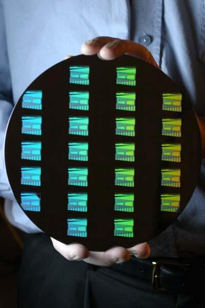
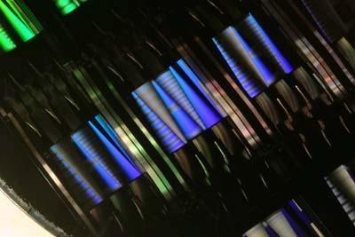
5 Photolithographically Scribed Planar Holograms (SiO 2 on Si)
6 Photolithographic Nanofab pathway Computer Design and Tape-Out Render Computed Design (Laserwriter) nm pixel full spatial coherence Device Fab (Silicon, Glass) 4x Reduction DUV Photolithography nm Master Fab 4x Reduction DUV Photolithography nm Device Fab nanoimprinting Device Fab molding/stamping Final Devices: cm-scale pattern, Full spatial coherence, nm feature size, Low-cost mass production via stepper/nanoimprint/injection molding

7 Laser Mask Writer Arbitrary Pattern, Submicron Pixels Micronic Laser Systems AB Write time (6 mask) 1 h 45 min Minimum main feature 220 nm Address grid 1.25 nm CD uniformity (global, 3 σ) 7 nm Registration (global, 3 σ) 15 nm

8 Modern DUV Reducing Stepper/Scanner Reduction Factor 4x (from mask) Resolution 65 nm Field Size 26 X 33 mm Throughput 122 wph 300 mm wafers 125 exposures
9 Slab-Waveguide Holographic Filter (Silica-on-Si) Core Thickness 2-4 microns Cladding Thickness 15 microns Materials Doped SiO 2 Substrate Silicon Wafer Device Length 0-2 cm Lines/cm 20,000 (1.5 µm) Line Spacing Λ λ/2n 7 top view out HBR in Cladding Core 7 Cladding cross sectional view (of slab waveguide)
10 Powerful Filter Passband Control ε(z) = reflection amplitude z = depth into device Throughput T(ν) 2 HBR T(ν ) ε ( z) exp{ 2π iν z/c} dz frequency (ν) out in
11 Spatial Coherence of Stepper-Written Holographic Filters Measured reflection bandwidth 0.08 nm Calculated weak signal width 0.05 nm ( 6 GHz) Spatial Coherence Length 1.5 cm Relative Power Measured Spectra of a 19-mm uniform grating transmission nm reflection 0.1 nm Resolution: ν c 15GHz 2nL nl( cm) Wavelength 10 GHz for 1-cm Silica Device
 Partial line writing (b) Interferometric contour placement (c) 500 nm line")
12 Binary Etch Compatible Apodization Approaches (Tailor Passband) Constant amplitude (a) Partial line writing (b) Interferometric contour placement (c) 500 nm line spacing
13 Partial-Fill GrayScale 2D Holographic Filter 1D Channel Grating Λ 100% integrated holographic grating 33% top view Partially Scribe Contours Percentage Scribed Controls Net Reflective Amplitude Λ out in w
14 Interferometric GrayScale Incident Field d o Reflected Field z What is net reflected field? δ i d o /2- δ i d o δ i E R E R ( δi, εi) exp(2ikoβi )cos(2koδi ) Phase Amplitude, β i = (z i -z 0 i ) z 0 i z i


15 Interferometric GrayScale - Visual Full Grating Delete every 3 rd line (resolution control) Displace for amplitude control 500 nm
16 Example of Apodization flat top CWDM filter 0 Reflected Power (db) unapodized apodized Linearly chirped holographic reflector with and without apodization Wavelength (nm)
17 Coupling Strength Issues Core Cladding Best Coupling (diffractive elements span mode) Diffractive elements of limited depth/aspect ratio Difficult to get strong coupling
18 Strong Coupling via Dual Core Construction Grating Layer (higher index) Shape edge for adiabatic transition Focus mode on grating For 1/e penetration depth, d, grating length L νtot 10GHz L( cm) d 2 ( cm ) d cm fabricated
19 Broad Bandwidth Reflector via Strong Coupling 0 69 nm Reflected Power (db) linear chirp linear chirp with apodization Wavelength (nm)
20 Losses Out-of-plane scattering (loss) In-plane scattering (guided) λ Cladding Core Cladding ρ 1 n n clad core Λ/2 No Losses! λ = Λ ( ) 1 ρ 2 Λ
21 Multiplexers
 Τ")


22 Coarse WDM Mux (only integrated solution) Τ (ν) 8 Τ 6 Τ 4 Τ 2 Τ 1 Τ 2 Τ 3 Τ 4 Τ 5 Τ 6 Τ 7 Τ IN Τ 1 Τ 3 Τ 5 Τ 7 r 18.8 mm
23 Polarization Properties

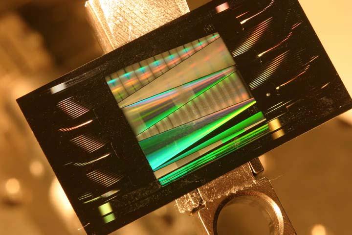
24 Close-up of Integrated HBR CWDM Mux

25 Integrated vs Discrete CWDM Mux Integrated CWDM mux Discrete TFF CWDM Mux

26 Photo of integrated holographic multiplexers Filter Sections Input Waveguides
27 Stacked Integrated Holographic Devices for Multiplexing Τ8 (ν) Τ6 Τ4 Τ2 Τ6 Τ7 Τ8 Τ Τ 5 Τ1 Τ2 Τ3 4 Stack upper cladding core IN lower cladding Τ1 Τ3 Τ5 Τ7 r Overlay Τ4(ν) Τ2 Interleave IN Τ1 Τ3 Slab Waveguide Λ d
28 8-channel, 100-GHz, HBR-based, Gaussian MUX 0 (a) Simulation (a) Simulation (constant index) Relative Insertion Loss (db) λ 1 λ 2 λ 3 λ 4 λ 5 λ 6 λ 7 λ 8-40 (b) Measurement Relative Insertion Loss (db) (b) (c) Measurement (1-channel) Simulation (apodization index coupling included) Wavelength (nm) Wavelength (nm)
29 4-channel, 50-GHz, Gaussian, HBR MUX 0 (a) Simulation -5 Relative Insertion Loss (db) (b) Measurement λ 1 λ 2 λ 3 λ db Insertion Loss Wavelength (nm)
30 Integrated Reflective Resonators
31 Integrated Reflective High-Q Resonator Input 4 mm Reflection Reflection (TM) HBR R = 73% Transmission (TM) HBR R = 73% Transmission Power (arb. units) Finesse: ~10 Losses < 1.2 % per pass Cavity Q almost 10 5 (reflectivity-limited) Surface figure λ/ Wavelength (nm) Wavelength (nm)

32 Photo of integrated holographic concentric cavity
33 Nearly Million-Q Integrated Reflective Resonator Reflected Power (arb. units) Wavelength (nm) Relative Reflected Power Wavelength (nm) 2.6 pm Q 10 6 Finesse 80 FSR = 220 pm FWHM = 2.6 pm Flatness Figure = 8 nm
34 Forward Scattering Holograms
35 Integrated Forward coupling Holographic lens Power Position (µm)
36 Photonic Crystals vs Holograms (Strong vs Weak Scattering) Photonic Crystals Space filling = lattice + basis = highly constrained structure. Control all optical modes = very short scattering length = high refractive index contrast. high losses to out-of-plane scattering Good for suppression of spontaneous radiative decay Volume Holograms Not space filling, translationally invarient, flexible structure Control specific signal modes, leave others alone = long scattering length = low refractive index contrast low out-of-plane scattering Good for optical signal filtering and routing in photonic circuits
37 Integrated Holographic Optical Interconnects
38 In-plane/Out-of-plane Coupling via Nanoprinted Diffractive Structures Input from Surface Mount Transmitter Output to Detector Diffractive Coupler Diffractive Coupler 2D Waveguide
39 Interconnection via Couplers and Photonic Transport Plane 1-D Solution: Fiber 2-D Solution: Channels waveguides wire analogs the optimal solution? What s the alternative? Photonic transport plane 1. slab waveguide 2. wavelength+wavefront selective I/O coupling along slab normal 3. contentionless links, point-to-point, point-to-multipoint 4. photonic localization only at source and sink 5. compatible with standard semiconductor fab 6. low effective index contrast for mode selectivity and low loss (anti-photonic bandgap) A C B A B D C D C cladding cladding Guiding diffractive structure core layer(s)
40 Low Cost Fabrication for Ubiquitous Photonics
41 Integrated Holographics, Replication, Plastics Litho Scribed Stamp/Mold UV phase mask write Upper Cladding (poured) UV writing beam Cladding Core Cladding Direct Grating Write Upper Cladding (poured) Cladding
42 Summary Fabrication advances open the door to planar volume holographics devices Functional equivalent of integrated thin film filters Multiplexers (small with flexible passband) Integrated reflective resonators (high finesse, high Q) Truly photonic integrated circuits Overlapping, delocalized signal paths Signal selection via mode-specific holographic structures Consistent with low cost volume manufacture DUV photolithography Nanoimprinting Many basic questions remaining to possible function, loss management, mode selectivity, non-linear effects, etc., remain.
43 LightSmyth Publications ( 1. T. W. Mossberg, Planar holographic optical processing devices, Opt. Lett. 26, (2001). 2. C. Greiner, D. Iazikov and T. W. Mossberg, Fourier-transform-limited performance of a lithographically-scribed planar holographic Bragg reflector, Photon. Technol. Lett. 16, (2004). 3. C. Greiner, D. Iazikov, and T. W. Mossberg, Lithgraphically-fabricated planar holographic Bragg reflectors, J. Lightwave Tech. 22, (2004). 4. D. Iazikov, C. Greiner, and T. W. Mossberg, Effective grayscale in lithographically scribed planar holographic Bragg reflectors, Appl. Opt. 43, (2004). 5. C. Greiner, T. W. Mossberg, and D. Iazikov, Bandpass engineering of lithographically-scribed channel-waveguide Bragg gratings, Opt. Lett. 29, (2004). 6. D. Iazikov, C. Greiner, and T. W. Mossberg, Apodizable integrated filters for coarse WDM and FTTH-type applications, J. Lightwave Tech. 22, (2004). 7. T. W. Mossberg, D. Iazikov, and C. Greiner, Planar-waveguide integrated spectral comparator, submitted to J. Opt. Soc. America A. 21, (2004). 8. C. Greiner, D. Iazikov and T. W. Mossberg, Wavelength-division multiplexing based on apodized planar holographic Bragg reflectors, Appl. Opt. 43, (2004). 9. C. Greiner, D. Iazikov and T. W. Mossberg, Low-loss silica-on-silicon two-dimensional Fabry Perot cavity based on holographic Bragg reflectors, Opt. Lett. 30, (2005). 10. T. W. Mossberg, C. Greiner, and D. Iazikov, Interferometric amplitude apodization of integrated gratings, Opt. Exp. 13, (2005). 11. Yue-Kai Haung, Varghese Baby, Paul R. Prucnal, Christoph M. Greiner, Dmitri Iazikov and Thomas W. Mossberg, Integrated holographic encoder for wavelength-hopping/time-spreading optical CDMA, Photon. Technol. Lett. 17, (2005). 12. Jose M. Castro, David F. Geraghty, Seppo Honkanen, Christoph M. Greiner, Dmitri Iazikov and Thomas W. Mossberg, Demonstration of mode conversion using anti-symmetric waveguide Bragg gratings, Optics Express 13, (2005). 13. T.W. Mossberg and M.G. Raymer, Optical code-division multiplexing: the intelligent optical solution, Opt.and Phot. News 12, (2001). 14. T. W. Mossberg, Lithographic holography in planar waveguides, SPIE Holography Newsletter 12, (2001). 15. T. W. Mossberg, C. Greiner, and D. Iazikov, Holographic Bragg reflectors, photonic bandgaps, and photonic integrated circuits, Optics and Photonics News 15, (2004). 16. T. Mossberg, C. Greiner and D. Iazikov, Submicron photolithography opens new areas of holographic design, Laser Focus World 40, (2004). 17. T.W. Mossberg, D. Iazikov, C.M. Greiner, Impact of High-resolution photolithography on integrated photonics, Microlithography World 14, 8 11 (2005).
Integrated Photonics based on Planar Holographic Bragg Reflectors
 Integrated Photonics based on Planar Holographic Bragg Reflectors C. Greiner *, D. Iazikov and T. W. Mossberg LightSmyth Technologies, Inc., 86 W. Park St., Ste 25, Eugene, OR 9741 ABSTRACT Integrated
Submicron planar waveguide diffractive photonics
 Invited Paper Submicron planar waveguide diffractive photonics T. W. Mossberg*, C. Greiner, and D. Iazikov LightSmyth Technologies, Inc., 86 West Park St., Suite 25, Eugene, OR 9741 ABSTRACT Recent advances
Ultra-small footprint silica-on-silicon WDM based on Holographic Bragg Reflectors
 Ultra-small footprint silica-on-silicon WDM based on Holographic Bragg Reflectors D. Iazikov, C. Greiner *, and T. W. Mossberg LightSmyth Technologies, Inc., 86 W. Park St., Ste 25, Eugene, OR 9741 ABSTRACT
Compact-footprint, focusing, lithographically-scribed planar holographic Bragg reflector
 Compact-footprint, focusing, lithographically-scribed planar holographic Bragg reflector C. Greiner *, D. Iazikov and T. W. Mossberg LightSmyth Technologies, Inc., 860 W. Park St., Ste 250, Eugene, OR
THE development of inexpensive yet robust and high-performance
 1402 JOURNAL OF LIGHTWAVE TECHNOLOGY, VOL. 22, NO. 5, MAY 2004 Apodizable Integrated Filters for Coarse WDM and FTTH-Type Applications D. Iazikov, Member, IEEE, C. Greiner, Member, IEEE, Member, OSA, and
Diffraction-limited performance of flat-substrate reflective imaging gratings patterned by DUV photolithography
 Diffraction-limited performance of flat-substrate reflective imaging gratings patterned by DUV photolithography Christoph M. Greiner, D. Iazikov, and T. W. Mossberg LightSmyth Technologies, 860 W Park
Bragg and fiber gratings. Mikko Saarinen
 Bragg and fiber gratings Mikko Saarinen 27.10.2009 Bragg grating - Bragg gratings are periodic perturbations in the propagating medium, usually periodic variation of the refractive index - like diffraction
Photonics and Optical Communication
 Photonics and Optical Communication (Course Number 300352) Spring 2007 Dr. Dietmar Knipp Assistant Professor of Electrical Engineering http://www.faculty.iu-bremen.de/dknipp/ 1 Photonics and Optical Communication
Single integrated device for optical CDMA code processing in dual-code environment
 Single integrated device for optical CDMA code processing in dual-code environment Yue-Kai Huang 1*, Ivan Glesk 1, Christoph M. Greiner, Dmitri Iazikov, Thomas W. Mossberg, Ting Wang 3, and Paul R. Prucnal
OPTICAL COMMUNICATIONS S
 OPTICAL COMMUNICATIONS S-108.3110 1 Course program 1. Introduction and Optical Fibers 2. Nonlinear Effects in Optical Fibers 3. Fiber-Optic Components 4. Transmitters and Receivers 5. Fiber-Optic Measurements
Silicon Photonic Device Based on Bragg Grating Waveguide
 Silicon Photonic Device Based on Bragg Grating Waveguide Hwee-Gee Teo, 1 Ming-Bin Yu, 1 Guo-Qiang Lo, 1 Kazuhiro Goi, 2 Ken Sakuma, 2 Kensuke Ogawa, 2 Ning Guan, 2 and Yong-Tsong Tan 2 Silicon photonics
Optical Communications and Networking 朱祖勍. Sept. 25, 2017
 Optical Communications and Networking Sept. 25, 2017 Lecture 4: Signal Propagation in Fiber 1 Nonlinear Effects The assumption of linearity may not always be valid. Nonlinear effects are all related to
Section 2: Lithography. Jaeger Chapter 2. EE143 Ali Javey Slide 5-1
 Section 2: Lithography Jaeger Chapter 2 EE143 Ali Javey Slide 5-1 The lithographic process EE143 Ali Javey Slide 5-2 Photolithographic Process (a) (b) (c) (d) (e) (f) (g) Substrate covered with silicon
Optical add drop multiplexers based on the antisymmetric waveguide Bragg grating
 Optical add drop multiplexers based on the antisymmetric waveguide Bragg grating Jose M. Castro, David F. Geraghty, Seppo Honkanen, Christoph M. Greiner, Dmitri Iazikov, and Thomas W. Mossberg A novel
Variable splitting ratio 2 2 MMI couplers using multimode waveguide holograms
 Variable splitting ratio 2 2 MMI couplers using multimode waveguide holograms Shuo-Yen Tseng, Canek Fuentes-Hernandez, Daniel Owens, and Bernard Kippelen Center for Organic Photonics and Electronics, School
Design and Analysis of Resonant Leaky-mode Broadband Reflectors
 846 PIERS Proceedings, Cambridge, USA, July 6, 8 Design and Analysis of Resonant Leaky-mode Broadband Reflectors M. Shokooh-Saremi and R. Magnusson Department of Electrical and Computer Engineering, University
AWG OPTICAL DEMULTIPLEXERS: FROM DESIGN TO CHIP. D. Seyringer
 AWG OPTICAL DEMULTIPLEXERS: FROM DESIGN TO CHIP D. Seyringer Research Centre for Microtechnology, Vorarlberg University of Applied Sciences, Hochschulstr. 1, 6850 Dornbirn, Austria, E-mail: dana.seyringer@fhv.at
Opto-VLSI-based reconfigurable photonic RF filter
 Research Online ECU Publications 29 Opto-VLSI-based reconfigurable photonic RF filter Feng Xiao Mingya Shen Budi Juswardy Kamal Alameh This article was originally published as: Xiao, F., Shen, M., Juswardy,
Silicon photonic devices based on binary blazed gratings
 Silicon photonic devices based on binary blazed gratings Zhiping Zhou Li Yu Optical Engineering 52(9), 091708 (September 2013) Silicon photonic devices based on binary blazed gratings Zhiping Zhou Li Yu
Lithography. 3 rd. lecture: introduction. Prof. Yosi Shacham-Diamand. Fall 2004
 Lithography 3 rd lecture: introduction Prof. Yosi Shacham-Diamand Fall 2004 1 List of content Fundamental principles Characteristics parameters Exposure systems 2 Fundamental principles Aerial Image Exposure
Section 2: Lithography. Jaeger Chapter 2 Litho Reader. The lithographic process
 Section 2: Lithography Jaeger Chapter 2 Litho Reader The lithographic process Photolithographic Process (a) (b) (c) (d) (e) (f) (g) Substrate covered with silicon dioxide barrier layer Positive photoresist
Introduction Fundamentals of laser Types of lasers Semiconductor lasers
 ECE 5368 Introduction Fundamentals of laser Types of lasers Semiconductor lasers Introduction Fundamentals of laser Types of lasers Semiconductor lasers How many types of lasers? Many many depending on
Section 2: Lithography. Jaeger Chapter 2 Litho Reader. EE143 Ali Javey Slide 5-1
 Section 2: Lithography Jaeger Chapter 2 Litho Reader EE143 Ali Javey Slide 5-1 The lithographic process EE143 Ali Javey Slide 5-2 Photolithographic Process (a) (b) (c) (d) (e) (f) (g) Substrate covered
Index. Cambridge University Press Silicon Photonics Design Lukas Chrostowski and Michael Hochberg. Index.
 absorption, 69 active tuning, 234 alignment, 394 396 apodization, 164 applications, 7 automated optical probe station, 389 397 avalanche detector, 268 back reflection, 164 band structures, 30 bandwidth
A novel tunable diode laser using volume holographic gratings
 A novel tunable diode laser using volume holographic gratings Christophe Moser *, Lawrence Ho and Frank Havermeyer Ondax, Inc. 85 E. Duarte Road, Monrovia, CA 9116, USA ABSTRACT We have developed a self-aligned
CHAPTER 2 POLARIZATION SPLITTER- ROTATOR BASED ON A DOUBLE- ETCHED DIRECTIONAL COUPLER
 CHAPTER 2 POLARIZATION SPLITTER- ROTATOR BASED ON A DOUBLE- ETCHED DIRECTIONAL COUPLER As we discussed in chapter 1, silicon photonics has received much attention in the last decade. The main reason is
Longitudinal mode selection in laser cavity by moiré volume Bragg grating
 Longitudinal mode selection in laser cavity by moiré volume Bragg grating Daniel Ott* a, Vasile Rotar a, Julien Lumeau a, Sergiy Mokhov a, Ivan Divliansky a, Aleksandr Ryasnyanskiy b, Nikolai Vorobiev
On-chip interrogation of a silicon-on-insulator microring resonator based ethanol vapor sensor with an arrayed waveguide grating (AWG) spectrometer
 spectrometer") On-chip interrogation of a silicon-on-insulator microring resonator based ethanol vapor sensor with an arrayed waveguide grating (AWG) spectrometer Nebiyu A. Yebo* a, Wim Bogaerts, Zeger Hens b,roel Baets
On-chip interrogation of a silicon-on-insulator microring resonator based ethanol vapor sensor with an arrayed waveguide grating (AWG) spectrometer Nebiyu A. Yebo* a, Wim Bogaerts, Zeger Hens b,roel Baets
CHIRPED FIBER BRAGG GRATING (CFBG) BY ETCHING TECHNIQUE FOR SIMULTANEOUS TEMPERATURE AND REFRACTIVE INDEX SENSING
 BY ETCHING TECHNIQUE FOR SIMULTANEOUS TEMPERATURE AND REFRACTIVE INDEX SENSING") CHIRPED FIBER BRAGG GRATING (CFBG) BY ETCHING TECHNIQUE FOR SIMULTANEOUS TEMPERATURE AND REFRACTIVE INDEX SENSING Siti Aisyah bt. Ibrahim and Chong Wu Yi Photonics Research Center Department of Physics,
CHIRPED FIBER BRAGG GRATING (CFBG) BY ETCHING TECHNIQUE FOR SIMULTANEOUS TEMPERATURE AND REFRACTIVE INDEX SENSING Siti Aisyah bt. Ibrahim and Chong Wu Yi Photonics Research Center Department of Physics,
Figure 1 Basic waveguide structure
 Recent Progress in SOI Nanophotonic Waveguides D. Van Thourhout, P. Dumon, W. Bogaerts, G. Roelkens, D. Taillaert, G. Priem, R. Baets IMEC-Ghent University, Department of Information Technology, St. Pietersnieuwstraat
S Optical Networks Course Lecture 2: Essential Building Blocks
 S-72.3340 Optical Networks Course Lecture 2: Essential Building Blocks Edward Mutafungwa Communications Laboratory, Helsinki University of Technology, P. O. Box 2300, FIN-02015 TKK, Finland Tel: +358 9
MICROCHIP MANUFACTURING by S. Wolf
 MICROCHIP MANUFACTURING by S. Wolf Chapter 19 LITHOGRAPHY II: IMAGE-FORMATION and OPTICAL HARDWARE 2004 by LATTICE PRESS CHAPTER 19 - CONTENTS Preliminaries: Wave- Motion & The Behavior of Light Resolution
Silicon Light Machines Patents
 820 Kifer Road, Sunnyvale, CA 94086 Tel. 408-240-4700 Fax 408-456-0708 www.siliconlight.com Silicon Light Machines Patents USPTO No. US 5,808,797 US 5,841,579 US 5,798,743 US 5,661,592 US 5,629,801 US
Characterization of Photonic Structures with CST Microwave Studio. CST UGM 2010 Darmstadt
 Characterization of Photonic Structures with CST Microwave Studio Stefan Prorok, Jan Hendrik Wülbern, Jan Hampe, Hooi Sing Lee, Alexander Petrov and Manfred Eich, Institute of Optical and Electronic Materials
On-chip Si-based Bragg cladding waveguide with high index contrast bilayers
 On-chip Si-based Bragg cladding waveguide with high index contrast bilayers Yasha Yi, Shoji Akiyama, Peter Bermel, Xiaoman Duan, and L. C. Kimerling Massachusetts Institute of Technology, 77 Massachusetts
Narrowing spectral width of green LED by GMR structure to expand color mixing field
 Narrowing spectral width of green LED by GMR structure to expand color mixing field S. H. Tu 1, Y. C. Lee 2, C. L. Hsu 1, W. P. Lin 1, M. L. Wu 1, T. S. Yang 1, J. Y. Chang 1 1. Department of Optical and
DWDM FILTERS; DESIGN AND IMPLEMENTATION
 DWDM FILTERS; DESIGN AND IMPLEMENTATION 1 OSI REFERENCE MODEL PHYSICAL OPTICAL FILTERS FOR DWDM SYSTEMS 2 AGENDA POINTS NEED CHARACTERISTICS CHARACTERISTICS CLASSIFICATION TYPES PRINCIPLES BRAGG GRATINGS
ABSTRACT 1. INTRODUCTION
 High spectral contrast filtering produced by multiple pass reflections from paired Bragg gratings in PTR glass Daniel Ott*, Marc SeGall, Ivan Divliansky, George Venus, Leonid Glebov CREOL, College of Optics
Ultra-Low-Loss Athermal AWG Module with a Large Number of Channels
 Ultra-Low-Loss Athermal AWG Module with a Large Number of Channels by Junichi Hasegawa * and Kazutaka Nara * There is an urgent need for an arrayed waveguide grating (AWG), the device ABSTRACT that handles
Realization of Polarization-Insensitive Optical Polymer Waveguide Devices
 644 Realization of Polarization-Insensitive Optical Polymer Waveguide Devices Kin Seng Chiang,* Sin Yip Cheng, Hau Ping Chan, Qing Liu, Kar Pong Lor, and Chi Kin Chow Department of Electronic Engineering,
Large aperture tunable ultra narrow band Fabry-Perot-Bragg filter
 Large aperture tunable ultra narrow band Fabry-Perot-Bragg filter Julien Lumeau *, Vadim Smirnov, Fabien Lemarchand 3, Michel Lequime 3 and Leonid B. Glebov School of Optics/CREOL, University of Central
Confocal Imaging Through Scattering Media with a Volume Holographic Filter
 Confocal Imaging Through Scattering Media with a Volume Holographic Filter Michal Balberg +, George Barbastathis*, Sergio Fantini % and David J. Brady University of Illinois at Urbana-Champaign, Urbana,
The range of applications which can potentially take advantage of CGH is very wide. Some of the
 CGH fabrication techniques and facilities J.N. Cederquist, J.R. Fienup, and A.M. Tai Optical Science Laboratory, Advanced Concepts Division Environmental Research Institute of Michigan P.O. Box 8618, Ann
Transmitting Light: Fiber-optic and Free-space Communications Holography
 1 Lecture 9 Transmitting Light: Fiber-optic and Free-space Communications Holography 2 Wireless Phone Calls http://havilandtelconews.com/2011/10/the-reality-behind-wireless-networks/ 3 Undersea Cable and
Achievement of Arbitrary Bandwidth of a Narrow Bandpass Filter
 Achievement of Arbitrary Bandwidth of a Narrow Bandpass Filter Cheng-Chung ee, Sheng-ui Chen, Chien-Cheng Kuo and Ching-Yi Wei 2 Department of Optics and Photonics/ Thin Film Technology Center, National
Module 19 : WDM Components
 Module 19 : WDM Components Lecture : WDM Components - I Part - I Objectives In this lecture you will learn the following WDM Components Optical Couplers Optical Amplifiers Multiplexers (MUX) Insertion
 Chapter 5 5.1 What are the factors that determine the thickness of a polystyrene waveguide formed by spinning a solution of dissolved polystyrene onto a substrate? density of polymer concentration of polymer
Grating-waveguide structures and their applications in high-power laser systems
 Grating-waveguide structures and their applications in high-power laser systems Marwan Abdou Ahmed*, Martin Rumpel, Tom Dietrich, Stefan Piehler, Benjamin Dannecker, Michael Eckerle, and Thomas Graf Institut
Part 5-1: Lithography
 Part 5-1: Lithography Yao-Joe Yang 1 Pattern Transfer (Patterning) Types of lithography systems: Optical X-ray electron beam writer (non-traditional, no masks) Two-dimensional pattern transfer: limited
Semiconductor Optical Communication Components and Devices Lecture 18: Introduction to Diode Lasers - I
 Semiconductor Optical Communication Components and Devices Lecture 18: Introduction to Diode Lasers - I Prof. Utpal Das Professor, Department of lectrical ngineering, Laser Technology Program, Indian Institute
Plane wave excitation by taper array for optical leaky waveguide antenna
 LETTER IEICE Electronics Express, Vol.15, No.2, 1 6 Plane wave excitation by taper array for optical leaky waveguide antenna Hiroshi Hashiguchi a), Toshihiko Baba, and Hiroyuki Arai Graduate School of
Ultra-compact, flat-top demultiplexer using anti-reflection contra-directional couplers for CWDM networks on silicon
 Ultra-compact, flat-top demultiplexer using anti-reflection contra-directional couplers for CWDM networks on silicon Wei Shi, Han Yun, Charlie Lin, Mark Greenberg, Xu Wang, Yun Wang, Sahba Talebi Fard,
A tunable Si CMOS photonic multiplexer/de-multiplexer
 A tunable Si CMOS photonic multiplexer/de-multiplexer OPTICS EXPRESS Published : 25 Feb 2010 MinJae Jung M.I.C.S Content 1. Introduction 2. CMOS photonic 1x4 Si ring multiplexer Principle of add/drop filter
Optical Amplifiers Photonics and Integrated Optics (ELEC-E3240) Zhipei Sun Photonics Group Department of Micro- and Nanosciences Aalto University
 Zhipei Sun Photonics Group Department of Micro- and Nanosciences Aalto University") Photonics Group Department of Micro- and Nanosciences Aalto University Optical Amplifiers Photonics and Integrated Optics (ELEC-E3240) Zhipei Sun Last Lecture Topics Course introduction Ray optics & optical
Photonics Group Department of Micro- and Nanosciences Aalto University Optical Amplifiers Photonics and Integrated Optics (ELEC-E3240) Zhipei Sun Last Lecture Topics Course introduction Ray optics & optical
Property improvement of flat-top 50 GHz-88 ch arrayed waveguide grating using phase correction waveguides
 Property improvement of flat-top 50 GHz-88 ch arrayed waveguide grating using phase correction waveguides Kazutaka Nara 1a) and Noritaka Matsubara 2 1 FITEL Photonics Laboratory, Furukawa Electric Co.,
2. Pulsed Acoustic Microscopy and Picosecond Ultrasonics
 1st International Symposium on Laser Ultrasonics: Science, Technology and Applications July 16-18 2008, Montreal, Canada Picosecond Ultrasonic Microscopy of Semiconductor Nanostructures Thomas J GRIMSLEY
Optical Fibers p. 1 Basic Concepts p. 1 Step-Index Fibers p. 2 Graded-Index Fibers p. 4 Design and Fabrication p. 6 Silica Fibers p.
 Preface p. xiii Optical Fibers p. 1 Basic Concepts p. 1 Step-Index Fibers p. 2 Graded-Index Fibers p. 4 Design and Fabrication p. 6 Silica Fibers p. 6 Plastic Optical Fibers p. 9 Microstructure Optical
Optical RI sensor based on an in-fiber Bragg grating. Fabry-Perot cavity embedded with a micro-channel
 Optical RI sensor based on an in-fiber Bragg grating Fabry-Perot cavity embedded with a micro-channel Zhijun Yan *, Pouneh Saffari, Kaiming Zhou, Adedotun Adebay, Lin Zhang Photonic Research Group, Aston
Optical Fiber Devices and Their Applications
 Optical Fiber Devices and Their Applications Yutaka SASAKI Faculty of Engineering Ibaraki University --, Nakanarusawa-cho, Hitachi, Ibaraki 6-85, Japan ABSTRACT: - Recent progress in research on optical
Convergence Challenges of Photonics with Electronics
 Convergence Challenges of Photonics with Electronics Edward Palen, Ph.D., P.E. PalenSolutions - Optoelectronic Packaging Consulting www.palensolutions.com palensolutions@earthlink.net 415-850-8166 October
Micro-sensors - what happens when you make "classical" devices "small": MEMS devices and integrated bolometric IR detectors
 Micro-sensors - what happens when you make "classical" devices "small": MEMS devices and integrated bolometric IR detectors Dean P. Neikirk 1 MURI bio-ir sensors kick-off 6/16/98 Where are the targets
Hybrid Integration Technology of Silicon Optical Waveguide and Electronic Circuit
 Hybrid Integration Technology of Silicon Optical Waveguide and Electronic Circuit Daisuke Shimura Kyoko Kotani Hiroyuki Takahashi Hideaki Okayama Hiroki Yaegashi Due to the proliferation of broadband services
Photonic Microwave Filter Employing an Opto- VLSI-Based Adaptive Optical Combiner
 Research Online ECU Publications 211 211 Photonic Microwave Filter Employing an Opto- VLSI-Based Adaptive Optical Combiner Haithem Mustafa Feng Xiao Kamal Alameh 1.119/HONET.211.6149818 This article was
Copyright 2000 by the Society of Photo-Optical Instrumentation Engineers.
 Copyright by the Society of Photo-Optical Instrumentation Engineers. This paper was published in the proceedings of Optical Microlithography XIII, SPIE Vol. 4, pp. 658-664. It is made available as an electronic
BEAM SHAPING OPTICS TO IMPROVE HOLOGRAPHIC AND INTERFEROMETRIC NANOMANUFACTURING TECHNIQUES Paper N405 ABSTRACT
 BEAM SHAPING OPTICS TO IMPROVE HOLOGRAPHIC AND INTERFEROMETRIC NANOMANUFACTURING TECHNIQUES Paper N5 Alexander Laskin, Vadim Laskin AdlOptica GmbH, Rudower Chaussee 9, 89 Berlin, Germany ABSTRACT Abstract
Single-Frequency, 2-cm, Yb-Doped Silica-Fiber Laser
 Single-Frequency, 2-cm, Yb-Doped Silica-Fiber Laser W. Guan and J. R. Marciante University of Rochester Laboratory for Laser Energetics The Institute of Optics Frontiers in Optics 2006 90th OSA Annual
Micro- and Nano-Technology... for Optics
 Micro- and Nano-Technology...... for Optics 3.2 Lithography U.D. Zeitner Fraunhofer Institut für Angewandte Optik und Feinmechanik Jena Printing on Stones Map of Munich Stone Print Contact Printing light
UNIT - 7 WDM CONCEPTS AND COMPONENTS
 UNIT - 7 WDM CONCEPTS AND COMPONENTS WDM concepts, overview of WDM operation principles, WDM standards, Mach-Zehender interferometer, multiplexer, Isolators and circulators, direct thin film filters, active
Ph 77 ADVANCED PHYSICS LABORATORY ATOMIC AND OPTICAL PHYSICS
 Ph 77 ADVANCED PHYSICS LABORATORY ATOMIC AND OPTICAL PHYSICS Diode Laser Characteristics I. BACKGROUND Beginning in the mid 1960 s, before the development of semiconductor diode lasers, physicists mostly
Fabrication of High-Speed Resonant Cavity Enhanced Schottky Photodiodes
 Fabrication of High-Speed Resonant Cavity Enhanced Schottky Photodiodes Abstract We report the fabrication and testing of a GaAs-based high-speed resonant cavity enhanced (RCE) Schottky photodiode. The
Computer Generated Holograms for Optical Testing
 Computer Generated Holograms for Optical Testing Dr. Jim Burge Associate Professor Optical Sciences and Astronomy University of Arizona jburge@optics.arizona.edu 520-621-8182 Computer Generated Holograms
Fast, Two-Dimensional Optical Beamscanning by Wavelength Switching T. K. Chan, E. Myslivets, J. E. Ford
 Photonics Systems Integration Lab University of California San Diego Jacobs School of Engineering Fast, Two-Dimensional Optical Beamscanning by Wavelength Switching T. K. Chan, E. Myslivets, J. E. Ford
NEXT GENERATION SILICON PHOTONICS FOR COMPUTING AND COMMUNICATION PHILIPPE ABSIL
 NEXT GENERATION SILICON PHOTONICS FOR COMPUTING AND COMMUNICATION PHILIPPE ABSIL OUTLINE Introduction Platform Overview Device Library Overview What s Next? Conclusion OUTLINE Introduction Platform Overview
Lecture: Integration of silicon photonics with electronics. Prepared by Jean-Marc FEDELI CEA-LETI
 Lecture: Integration of silicon photonics with electronics Prepared by Jean-Marc FEDELI CEA-LETI Context The goal is to give optical functionalities to electronics integrated circuit (EIC) The objectives
Principles of Optics for Engineers
 Principles of Optics for Engineers Uniting historically different approaches by presenting optical analyses as solutions of Maxwell s equations, this unique book enables students and practicing engineers
Compact two-mode (de)multiplexer based on symmetric Y-junction and Multimode interference waveguides
multiplexer based on symmetric Y-junction and Multimode interference waveguides") Compact two-mode (de)multiplexer based on symmetric Y-junction and Multimode interference waveguides Yaming Li, Chong Li, Chuanbo Li, Buwen Cheng, * and Chunlai Xue State Key Laboratory on Integrated Optoelectronics,
Compact two-mode (de)multiplexer based on symmetric Y-junction and Multimode interference waveguides Yaming Li, Chong Li, Chuanbo Li, Buwen Cheng, * and Chunlai Xue State Key Laboratory on Integrated Optoelectronics,
AMACH Zehnder interferometer (MZI) based on the
 based on the") 1284 JOURNAL OF LIGHTWAVE TECHNOLOGY, VOL. 23, NO. 3, MARCH 2005 Optimal Design of Planar Wavelength Circuits Based on Mach Zehnder Interferometers and Their Cascaded Forms Qian Wang and Sailing He, Senior
1284 JOURNAL OF LIGHTWAVE TECHNOLOGY, VOL. 23, NO. 3, MARCH 2005 Optimal Design of Planar Wavelength Circuits Based on Mach Zehnder Interferometers and Their Cascaded Forms Qian Wang and Sailing He, Senior
EE143 Fall 2016 Microfabrication Technologies. Lecture 3: Lithography Reading: Jaeger, Chap. 2
 EE143 Fall 2016 Microfabrication Technologies Lecture 3: Lithography Reading: Jaeger, Chap. 2 Prof. Ming C. Wu wu@eecs.berkeley.edu 511 Sutardja Dai Hall (SDH) 1-1 The lithographic process 1-2 1 Photolithographic
Lecture 6 Fiber Optical Communication Lecture 6, Slide 1
 Lecture 6 Optical transmitters Photon processes in light matter interaction Lasers Lasing conditions The rate equations CW operation Modulation response Noise Light emitting diodes (LED) Power Modulation
Investigation of ultrasmall 1 x N AWG for SOI- Based AWG demodulation integration microsystem
 University of Wollongong Research Online Faculty of Engineering and Information Sciences - Papers: Part A Faculty of Engineering and Information Sciences 2015 Investigation of ultrasmall 1 x N AWG for
Integrated grating-assisted coarse/dense WDM multiplexers
 Integrated grating-assisted coarse/dense WDM multiplexers Linping Shen *a, Chenglin Xu b, and Wei-Ping Huang b a Apollo Inc., 1057 Main Street W., Hamilton, ON, Canada L8S 1B7 * lpshen@apollophotonics.com;
New Waveguide Fabrication Techniques for Next-generation PLCs
 New Waveguide Fabrication Techniques for Next-generation PLCs Masaki Kohtoku, Toshimi Kominato, Yusuke Nasu, and Tomohiro Shibata Abstract New waveguide fabrication techniques will be needed to make highly
A Comparison of Optical Modulator Structures Using a Matrix Simulation Approach
 A Comparison of Optical Modulator Structures Using a Matrix Simulation Approach Kjersti Kleven and Scott T. Dunham Department of Electrical Engineering University of Washington 27 September 27 Outline
Copyright 2000 Society of Photo Instrumentation Engineers.
 Copyright 2000 Society of Photo Instrumentation Engineers. This paper was published in SPIE Proceedings, Volume 4043 and is made available as an electronic reprint with permission of SPIE. One print or
Synthesis of projection lithography for low k1 via interferometry
 Synthesis of projection lithography for low k1 via interferometry Frank Cropanese *, Anatoly Bourov, Yongfa Fan, Andrew Estroff, Lena Zavyalova, Bruce W. Smith Center for Nanolithography Research, Rochester
Optolith 2D Lithography Simulator
 2D Lithography Simulator Advanced 2D Optical Lithography Simulator 4/13/05 Introduction is a powerful non-planar 2D lithography simulator that models all aspects of modern deep sub-micron lithography It
APPLICATION OF VARIOUS TOOLS TO DESIGN, SIMULATE AND EVALUATE OPTICAL DEMULTIPLEXERS BASED ON AWG. Dana Seyringer and Johannes Edlinger
 APPLICATION OF VARIOUS TOOLS TO DESIGN, SIMULATE AND EVALUATE OPTICAL DEMULTIPLEXERS BASED ON AWG Dana Seyringer and Johannes Edlinger Research Centre for Microtechnology, Vorarlberg University of Applied
High-efficiency fiber-to-chip grating couplers realized using an advanced CMOS-compatible Silicon-On-Insulator platform
 High-efficiency fiber-to-chip grating couplers realized using an advanced CMOS-compatible Silicon-On-Insulator platform D. Vermeulen, 1, S. Selvaraja, 1 P. Verheyen, 2 G. Lepage, 2 W. Bogaerts, 1 P. Absil,
Adaptive multi/demultiplexers for optical signals with arbitrary wavelength spacing.
 Edith Cowan University Research Online ECU Publications Pre. 2011 2010 Adaptive multi/demultiplexers for optical signals with arbitrary wavelength spacing. Feng Xiao Edith Cowan University Kamal Alameh
Numerical analysis of a swift, high resolution wavelength monitor designed as a Generic Lightwave Integrated Chip (GLIC)
") Numerical analysis of a swift, high resolution wavelength monitor designed as a Generic Lightwave Integrated Chip (GLIC) John Ging and Ronan O Dowd Optoelectronics Research Centre University College Dublin,
Numerical analysis of a swift, high resolution wavelength monitor designed as a Generic Lightwave Integrated Chip (GLIC) John Ging and Ronan O Dowd Optoelectronics Research Centre University College Dublin,
Compact ellipsometer employing a static polarimeter module with arrayed polarizer and wave-plate elements
 Compact ellipsometer employing a static polarimeter module with arrayed polarizer and wave-plate elements Takashi Sato, 1 Takeshi Araki, 1 Yoshihiro Sasaki, 2 Toshihide Tsuru, 3 Toshiyasu Tadokoro, 1 and
Temporal phase mask encrypted optical steganography carried by amplified spontaneous emission noise
 Temporal phase mask encrypted optical steganography carried by amplified spontaneous emission noise Ben Wu, * Zhenxing Wang, Bhavin J. Shastri, Matthew P. Chang, Nicholas A. Frost, and Paul R. Prucnal
SPP waveguide sensors
 SPP waveguide sensors 1. Optical sensor - Properties - Surface plasmon resonance sensor - Long-range surface plasmon-polariton sensor 2. LR-SPP waveguide - SPP properties in a waveguide - Asymmetric double-electrode
Integrated photonic circuit in silicon on insulator for Fourier domain optical coherence tomography
 Integrated photonic circuit in silicon on insulator for Fourier domain optical coherence tomography Günay Yurtsever *,a, Pieter Dumon a, Wim Bogaerts a, Roel Baets a a Ghent University IMEC, Photonics
Electronically switchable Bragg gratings provide versatility
 Page 1 of 5 Electronically switchable Bragg gratings provide versatility Recent advances in ESBGs make them an optimal technological fabric for WDM components. ALLAN ASHMEAD, DigiLens Inc. The migration
SUPPLEMENTARY INFORMATION
 Optically reconfigurable metasurfaces and photonic devices based on phase change materials S1: Schematic diagram of the experimental setup. A Ti-Sapphire femtosecond laser (Coherent Chameleon Vision S)
Project Staff: Timothy A. Savas, Michael E. Walsh, Thomas B. O'Reilly, Dr. Mark L. Schattenburg, and Professor Henry I. Smith
 9. Interference Lithography Sponsors: National Science Foundation, DMR-0210321; Dupont Agreement 12/10/99 Project Staff: Timothy A. Savas, Michael E. Walsh, Thomas B. O'Reilly, Dr. Mark L. Schattenburg,
1. INTRODUCTION ABSTRACT
 Experimental verification of Sub-Wavelength Holographic Lithography physical concept for single exposure fabrication of complex structures on planar and non-planar surfaces Michael V. Borisov, Dmitry A.
Advances in Widely Tunable Lasers Richard Schatz Laboratory of Photonics Royal Institute of Technology
 Advances in Widely Tunable Lasers Richard Schatz Laboratory of Photonics Royal Institute of Technology Tunability of common semiconductor lasers Widely tunable laser types Syntune MGY laser: tuning principle
Half-tone proximity lithography
 Half-tone proximity lithography Torsten Harzendorf* a, Lorenz Stuerzebecher a, Uwe Vogler b, Uwe D. Zeitner a, Reinhard Voelkel b a Fraunhofer Institut für Angewandte Optik und Feinmechanik IOF, Albert