VERSATILE SILICON PHOTONIC PLATFORM FOR DATACOM AND COMPUTERCOM APPLICATIONS. B Szelag CEA-Leti
|
|
|
- Isaac Waters
- 5 years ago
- Views:
Transcription


1 VERSATILE SILICON PHOTONIC PLATFORM FOR DATACOM AND COMPUTERCOM APPLICATIONS B Szelag CEA-Leti
2 OUTLINE Silicon photonic : 200mm CMOS core technology towards 300mm Emergent needs vs core process Technological add-on #1 : 3D packaging Technological add-on #2 : Silicon Nitride circuits Technological add-on #3 : Hybrid III-V on silicon laser 2
 o Making photonic")
3 WHAT IS SILICON PHOTONIC? o Silicon photonic aims at integrating in the silicon microelectronic CMOS technology circuits and modules initially based on other technologies (InP, InGaAs, LNbO3, SiO2, ) o Making photonic integrated circuits on Silicon using CMOS process technology in a CMOS fab. o Merging photonics and CMOS. o Expected benefits: o Higher integration level o Low cost, high volume facilities o Access to mature packaging and EDA tools o WDM and scaling to >1 Tb/s o Solving electrical interconnect limits in Data centers, Supercomputers and ICs with higher capacity, lower cost optical interconnects 3

4 BUILDING BLOCKS FOR OPTICAL DATA TRANSMISSION 4


5 SILICON PHOTONIC CORE TECHNOLOGY DESCRIPTION 310nm SOI 193nm DUV lithography Multilevel silicon patterning Selective Germanium epitaxy Silicide Metal heater Planarized BEOL 2 AlCu routing levels UBM for Cu pillar assembly 5

6 SILICON PHOTONIC CORE TECHNOLOGY DESCRIPTION o Modulator junction formation & activation CMOS-based process with photonic dedicated optimizations o Define all the photonic devices o Various waveguide architectures o Photodetector patterning o Germanium selective epitaxy o Photodetector contact formation o Si Modulator contact silicidation CMOS standard process o Metal interconnection o Metal heater definition for l tuning 6

7 O-BAND DEVICE LIBRARY - EXAMPLE 7


8 EMERGENT NEEDS VS CORE PROCESS Co-integration with complex «host chips» FPGA or switches with optical IOs Manycore computers architectures Silicon Photonics address circuits of increasing complexity Hundreds of optical functions on a chip Ease routing using multilayer photonics Requires dedicated PDK in EDA tools Broadband coupling required for WDM modules Thermal constraints Laser source integration Several competing technologies Direct bonding approach : require CMOS compatibility 8


9 ADD-ON #1 : 3D PACKAGING High data rate silicon photonics based module must be considered as an RF module with an E/O or O/E convertor: RF packaging solutions are needed Si photonic platform must integrate Microbumps/Micropillars and/or TSV MicroBump/Micropillars High Datarate Modules o 50 µm pitch o Copper pillar with eutectic solder o C2W or C2C assembly o Low parasitics Reflective Tx for FTTH (EU FABULOUS project) Low power 25Gbps photoreceiver EIC 0.8 x 1.3 mm² 4 25Gbps receiver module QAM16 transmission on a single fiber Dedicated MZM segmented CMOS driver Straullu et al., ECOC PDP, 2016 Menezo et al., JLT, 34,10, µm pitch microbump 170 fj/bit -15 dbm sensitivity TIA design : Caltech Saaedi et al.. J. Lightwave Tech., 2015 WDM and SDM versions < -12dBm sensitivity at 10-9 BER EIC with 4pJ/bit consumption TIA design : ST microelectronics Bernabé et al., OIC 2016, Paper MB3 Castany et al., ESTC


10 ADD-ON #1 : 3D PACKAGING High data rate silicon photonics based module must be considered as an RF module with an E/O or O/E convertor: RF packaging solutions are needed Si photonic platform must integrate Microbumps/Micropillars and/or TSV Through Silicon Vias Abs(S12) TSV System-in-package WB TSV last on SOI wafer TSV vs WB on Transmission performances S. Bernabé, K. Rida, S. Menezo, IEEE Trans. Comp. Mfg and Pkg, 2016 L. Fourneaud, Internal report 10
 less sensitive to roughness and fabrication imperfections lower propagation losses Low thermo-optic coefficient ( ~2x10⁻⁵ K -1 ) Temperature quasi-insensitive devices for data center environment")
11 ADD-ON #2: SILICON-NITRIDE AS A PHOTONIC LAYER SiN Si SiO2 Si bulk n=1.88 n=3.5 Why Silicon nitride: Low refractive index (n SiN = 1.88) less sensitive to roughness and fabrication imperfections lower propagation losses Low thermo-optic coefficient ( ~2x10⁻⁵ K -1 ) Temperature quasi-insensitive devices for data center environment Objective: CWDM transceiver in the O-band ( nm) CWDM: Coarse Wavelength Division Multiplexing. 4 channels (= 4λ) with 20nm spacing. No temperature control of the lasers. Si-SiN platform: Active properties of Si and passive properties of SiN Si Si-SiN transition and waveguide Temperature insensitive SiN multiplexer Q. Wilmart el al., in Proc. of SPIE Phot. West 2018 SiN Broadband Si-SiN fiber grating coupler 11
 Oxide deposition 200nm SiN deposition")

 300nm 200nm Q. Wilmart el al., in Proc.")
12 SOI 300nm BOX 2µm SI-SIN FABRICATION & PERFORMANCE 1 st encapsulation Planarization CMP stop on HM (nm) Oxide deposition 200nm SiN deposition (600nm PECVD 300 C) + patterning (DUV 248nm) Final encapsulation 600nm Low temperature deposition of SiN Si doping compatibility SiN waveguide propagation loss : 0.8 db/cm (in Si 1.5 db/cm) SiN thermo-optic coeff. : 1.7x10⁻⁵ K -1 (in Si 2x10⁻⁴ K -1 ) 300nm 200nm Q. Wilmart el al., in Proc. of SPIE Phot. West


13 MULTIPLE PHOTONIC LAYER INTEGRATION Si-SiN transitions for 3D photonic 0.09 db/transition 150µm side view (BPM simu) Low thermal sensitive SiN Mux/DeMux High-efficiency & wide bandwidth Si-SiNx grating coupler C. Sciancalepore et al., SSDM 2017 Q. Wilmart el al., in Proc. of SPIE Phot. West
 III-V bonding")

 o III-V material patterning, o Metallization of")

14 ADD-ON #3: III-V INTEGRATION ON SI-PHOTONIC CHIP o Growth of the III-V wafers (2, 3, 4 ) III-V bonding on processed SOI & InP substrate removal o Processing of SOI wafers 8 or 12 (modulators, detectors, passive devices, etc.) o III-V material patterning, o Metallization of lasers, modulators and detectors CMOS fab compatible processes needed to avoid wafer downsizing and maximize the functional SOI wafer surface. 14
 The high resolution laser cavity as well")
 Equivalent to multiple localized epitaxies Die")
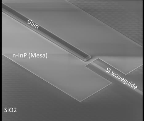
15 HETEROGENEOUS III-V INTEGRATION Components Laser Electro-absorption modulator Semiconductor optical amplifier To use the advantage of each material properties: Optical gain is provided by the III-V (InP/InGaAsP QWs or AlGaInAs) The high resolution laser cavity as well as the PIC is fabricated in a 200/300mm Silicon platform (CMOS planar technology) III-V wafer bonding To localize III-V by die-to-wafer bonding Highly flexible approach (multiple laser-l in the O+C+L bands / PD / EAM) Equivalent to multiple localized epitaxies Die bonding 15


 7,00 5,25 3,50 1,75 Si-waveguide")
 for T: 10 to 60 C Rs= 7.5 W Lasing turn-on voltage : 1.")


, 8489 (2015) T. Ferrotti et al.")
16 INTEGRATED HYBRID III-V/SI LASER PAST RESULTS Hybrid 1,55µm Hybrid 1,31µm 25Gb/s laser + MZM transmitter Fiber coupled optical power (mw) J(kA/cm²) 0,0 0,8 1,7 2,5 3,3 4,2 5,0 5,8 6,7 7,5 8,3 5,5 19,25 5,0 10 C 20 C 17,50 4,5 30 C 15,75 4,0 40 C 14,00 3,5 50 C 12,25 3,0 60 C 10,50 65 C 2,5 8,75 2,0 1,5 1,0 0,5 0, Current (ma) 7,00 5,25 3,50 1,75 Si-waveguide power (mw) 0,00 A. CW operation (>60 C) I th : 17-60mA ( ka.cm -2 ) for T: 10 to 60 C Rs= 7.5 W Lasing turn-on voltage : 1.0 V P -Si-waveguide > 14 mw (20 C) P -fiber > 4 mw (20 C) SMSR > 40 db A.Descos et al., ECOC 2013 CW operation (>55 C) Ith: 30-50mA Rs= 15 W Lasing turn-on voltage : 1.2 V P-Si-waveguide > 20 mw (20 C) P-fiber > 3 mw (20 C) SMSR > 40 db H. Duprez et al., Opt. Express 23(7), 8489 (2015) T. Ferrotti et al., SSDM, (2016) Co-integration hybrid IIIV/Silicon DBR laser + silicon Mach-Zehnder modulator. 25Gb/s transmission at 1.3µm up to 10km. 16


17 III-V INTEGRATION ON SI: TOWARD LSI CMOS COMPATIBLE PROCESS 1. Process & Materials Patterning Contact on III-V Multi level BEOL III-V Die Bonding 2. Laser Topography III-V stack thickness=4µm vs. PMD thickness=1µm 3. SOI Substrate SOI for laser: 500nm vs. SOI platform: 310nm 4. Laser integration impact on other devices 17


18 LARGE SCALE INTEGRATION CMOS FRIENDLY PROCESS Multilevel planar BEOL Ohmic contacts on III-V materials III-V patterning Collective III-V die bonding B. Szelag et al., IEDM 2017 Localized silicon thickning 18


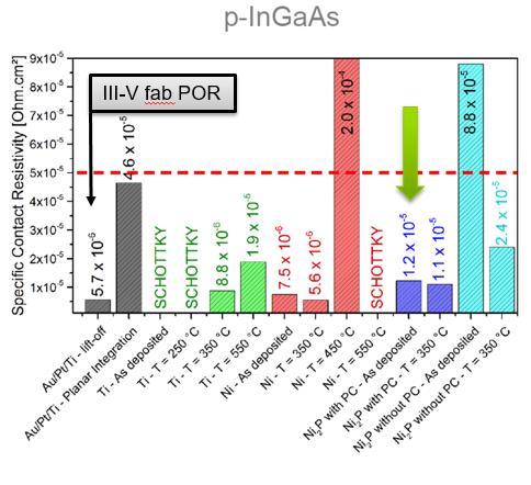
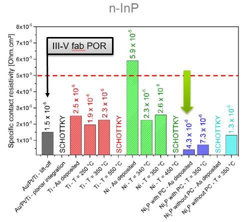

19 Ohmic contacts on III-V materials LARGE SCALE INTEGRATION CMOS FRIENDLY PROCESS Multilevel planar BEOL III-V patterning Silicon localized thickning 19

 @room")
20 FIRST DEMO ON 200MM SOI WAFER OPTICAL CHARACTERIZATION o Only 1 metal layer for this design o Ni-based N & P contacts Ith: 55-65mA Rs= 10 W Max P-Si-waveguide > 3 mw Max P-fiber 1 mw SMSR > 40 db (best temperature 20

21 COLLECTIVE DIE BONDING WITH SILICON HOLDERS +Efficient cleaning +Very high transfer rate >95% +Bonding Yield~100% +CAD2MASK Holder mask generation during PIC design - Additional cost for holder fabrication 21


22 COLLECTIVE DIE BONDING WITH SI HOLDER - EXAMPLE After die Bonding After InP grinding Acoustic characterization P01 P02 P03 P04 o Transferred die: 99 % 99% 99% 70% o Transferred die without defects: 75 % 73% 73% 52% o Transferred die & bonded on more than 99% of their surface: 87 % 84% 88% 62% o Transferred die & bonded on more than 95% of their surface : 91 % 85% 90% 64% 22


23 BACKSIDE INTEGRATION (BSI) CONCEPT Problems: 1. III-V based device integration with not change on the baseline photonic platform (BEOL) 2. III-V based device integration compatible with a co-integration of SiN devices Solution: III-V post processing on the backside of the full silicon photonic platform 23


24 HYBRID LASER BSI DEMONSTRATION o Integration scheme compatible with any photonic platform o No impact on the Silicon photonic platform o Modular integration o Si photonic platform and laser integration can be done in 2 different fabs o Only way to have 3D photonic (SiN or Si level on top of SOI) and laser on the same die o EIC and opposite sides of the PIC o Demo: Passive + BSI DBR laser done with 100mm process (J. Durel et Al, IEDM 2016) 24


25 CONCLUSION Silicon Photonics CORE process 3D Photonics (SiN/Si, Si/Si) III-V on Silicon (FSI or BSI) 3D packaging 200mm III-V CMOS compatible process Large scale die to wafer bonding 25


26 Acknowledgements to : IRT Photonics & H2020 COSMICC Thank you Leti, technology research institute Commissariat à l énergie atomique et aux énergies alternatives Minatec Campus 17 rue des Martyrs Grenoble Cedex France
Silicon Photonics : Towards Heterogeneous and Multi-layer Integration for High Density Circuits
 Silicon Photonics : Towards Heterogeneous and Multi-layer Integration for High Density Circuits Stéphane Bernabé, Ségolène Olivier, Bertrand Szelag, Daivid Fowler, Christophe Kopp OPTICS, Dresden, 23-03-16
Lecture: Integration of silicon photonics with electronics. Prepared by Jean-Marc FEDELI CEA-LETI
 Lecture: Integration of silicon photonics with electronics Prepared by Jean-Marc FEDELI CEA-LETI Context The goal is to give optical functionalities to electronics integrated circuit (EIC) The objectives
Si and InP Integration in the HELIOS project
 Si and InP Integration in the HELIOS project J.M. Fedeli CEA-LETI, Grenoble ( France) ECOC 2009 1 Basic information about HELIOS HELIOS photonics ELectronics functional Integration on CMOS www.helios-project.eu
NEXT GENERATION SILICON PHOTONICS FOR COMPUTING AND COMMUNICATION PHILIPPE ABSIL
 NEXT GENERATION SILICON PHOTONICS FOR COMPUTING AND COMMUNICATION PHILIPPE ABSIL OUTLINE Introduction Platform Overview Device Library Overview What s Next? Conclusion OUTLINE Introduction Platform Overview
Opportunities and challenges of silicon photonics based System-In-Package
 Opportunities and challenges of silicon photonics based System-In-Package ECTC 2014 Panel session : Emerging Technologies and Market Trends of Silicon Photonics Speaker : Stéphane Bernabé (Leti Photonics
Silicon Photonics: an Industrial Perspective
 Silicon Photonics: an Industrial Perspective Antonio Fincato Advanced Programs R&D, Cornaredo, Italy OUTLINE 2 Introduction Silicon Photonics Concept 300mm (12 ) Photonic Process Main Silicon Photonics
Photonic modules for data centers Leti SAMTEC FINAL p Photonic modules for data centers require cutting edge technologies
 Photonic modules for data centers Leti SAMTEC FINAL p. 1 072817 Photonic modules for data centers require cutting edge technologies by Stéphane Bernabé, Olivier Castany, Bertrand Szelag, Benoît Charbonnier
IEEE JOURNAL OF SELECTED TOPICS IN QUANTUM ELECTRONICS 2010 Silicon Photonic Circuits: On-CMOS Integration, Fiber Optical Coupling, and Packaging
 IEEE JOURNAL OF SELECTED TOPICS IN QUANTUM ELECTRONICS 2010 Silicon Photonic Circuits: On-CMOS Integration, Fiber Optical Coupling, and Packaging Christophe Kopp, St ephane Bernab e, Badhise Ben Bakir,
A 3.9 ns 8.9 mw 4 4 Silicon Photonic Switch Hybrid-Integrated with CMOS Driver
 A 3.9 ns 8.9 mw 4 4 Silicon Photonic Switch Hybrid-Integrated with CMOS Driver A. Rylyakov, C. Schow, B. Lee, W. Green, J. Van Campenhout, M. Yang, F. Doany, S. Assefa, C. Jahnes, J. Kash, Y. Vlasov IBM
Silicon photonics on 3 and 12 μm thick SOI for optical interconnects Timo Aalto VTT Technical Research Centre of Finland
 Silicon photonics on 3 and 12 μm thick SOI for optical interconnects Timo Aalto VTT Technical Research Centre of Finland 5th International Symposium for Optical Interconnect in Data Centres in ECOC, Gothenburg,
Silicon Photonics Photo-Detector Announcement. Mario Paniccia Intel Fellow Director, Photonics Technology Lab
 Silicon Photonics Photo-Detector Announcement Mario Paniccia Intel Fellow Director, Photonics Technology Lab Agenda Intel s Silicon Photonics Research 40G Modulator Recap 40G Photodetector Announcement
New advances in silicon photonics Delphine Marris-Morini
 New advances in silicon photonics Delphine Marris-Morini P. Brindel Alcatel-Lucent Bell Lab, Nozay, France New Advances in silicon photonics D. Marris-Morini, L. Virot*, D. Perez-Galacho, X. Le Roux, D.
Electronic-Photonic ICs for Low Cost and Scalable Datacenter Solutions
 Electronic-Photonic ICs for Low Cost and Scalable Datacenter Solutions Christoph Theiss, Director Packaging Christoph.Theiss@sicoya.com 1 SEMICON Europe 2016, October 27 2016 Sicoya Overview Spin-off from
Introduction and concepts Types of devices
 ECE 6323 Introduction and concepts Types of devices Passive splitters, combiners, couplers Wavelength-based devices for DWDM Modulator/demodulator (amplitude and phase), compensator (dispersion) Others:
An Example Design using the Analog Photonics Component Library. 3/21/2017 Benjamin Moss
 An Example Design using the Analog Photonics Component Library 3/21/2017 Benjamin Moss Component Library Elements Passive Library Elements: Component Current specs 1 Edge Couplers (Si)
Innovations in Photonic Integration Platforms
 Innovations in Photonic Integration Platforms September 20, 20 Burgeoning Growth Demand Disruptive Technology Video content is fast becoming a larger percentage of total internet traffic 50% Video services
Heinrich-Hertz-Institut Berlin
 NOVEMBER 24-26, ECOLE POLYTECHNIQUE, PALAISEAU OPTICAL COUPLING OF SOI WAVEGUIDES AND III-V PHOTODETECTORS Ludwig Moerl Heinrich-Hertz-Institut Berlin Photonic Components Dept. Institute for Telecommunications,,
New silicon photonics technology delivers faster data traffic in data centers
 Edition May 2017 Silicon Photonics, Photonics New silicon photonics technology delivers faster data traffic in data centers New transceiver with 10x higher bandwidth than current transceivers. Today, the
Convergence Challenges of Photonics with Electronics
 Convergence Challenges of Photonics with Electronics Edward Palen, Ph.D., P.E. PalenSolutions - Optoelectronic Packaging Consulting www.palensolutions.com palensolutions@earthlink.net 415-850-8166 October
SiGe BiCMOS and Photonic technologies for high frequency and communication applications Andreas Mai
 SiGe BiCMOS and Photonic technologies for high frequency and communication applications Andreas Mai Department Head Technology Outline Introduction & Motivation SiGe HBT device developments for high RF
Silicon Photonics Technology Platform To Advance The Development Of Optical Interconnects
 Silicon Photonics Technology Platform To Advance The Development Of Optical Interconnects By Mieke Van Bavel, science editor, imec, Belgium; Joris Van Campenhout, imec, Belgium; Wim Bogaerts, imec s associated
ECEN689: Special Topics in Optical Interconnects Circuits and Systems Spring 2016
 ECEN689: Special Topics in Optical Interconnects Circuits and Systems Spring 2016 Lecture 1: Introduction Sam Palermo Analog & Mixed-Signal Center Texas A&M University Class Topics System and design issues
Silicon photonics with low loss and small polarization dependency. Timo Aalto VTT Technical Research Centre of Finland
 Silicon photonics with low loss and small polarization dependency Timo Aalto VTT Technical Research Centre of Finland EPIC workshop in Tokyo, 9 th November 2017 VTT Technical Research Center of Finland
Silicon Photonics Transceivers for Hyper Scale Datacenters: Deployment and Roadmap
 Silicon Photonics Transceivers for Hyper Scale Datacenters: Deployment and Roadmap Peter De Dobbelaere Luxtera Inc. 09/19/2016 Luxtera Proprietary www.luxtera.com Luxtera Company Introduction $100B+ Shift
EE 232 Lightwave Devices Optical Interconnects
 EE 232 Lightwave Devices Optical Interconnects Sajjad Moazeni Department of Electrical Engineering & Computer Sciences University of California, Berkeley 1 Emergence of Optical Links US IT Map Hyper-Scale
Silicon Photonics in Optical Communications. Lars Zimmermann, IHP, Frankfurt (Oder), Germany
, Germany") Silicon Photonics in Optical Communications Lars Zimmermann, IHP, Frankfurt (Oder), Germany Outline IHP who we are Silicon photonics Photonic-electronic integration IHP photonic technology Conclusions
Silicon Photonics in Optical Communications Lars Zimmermann, IHP, Frankfurt (Oder), Germany Outline IHP who we are Silicon photonics Photonic-electronic integration IHP photonic technology Conclusions
High-speed Ge photodetector monolithically integrated with large cross silicon-on-insulator waveguide
 [ APPLIED PHYSICS LETTERS ] High-speed Ge photodetector monolithically integrated with large cross silicon-on-insulator waveguide Dazeng Feng, Shirong Liao, Roshanak Shafiiha. etc Contents 1. Introduction
Integrated Photonics using the POET Optical InterposerTM Platform
 Integrated Photonics using the POET Optical InterposerTM Platform Dr. Suresh Venkatesan CIOE Conference Shenzhen, China Sept. 5, 2018 POET Technologies Inc. TSXV: PUBLIC POET PTK.V Technologies Inc. PUBLIC
Index. Cambridge University Press Silicon Photonics Design Lukas Chrostowski and Michael Hochberg. Index.
 absorption, 69 active tuning, 234 alignment, 394 396 apodization, 164 applications, 7 automated optical probe station, 389 397 avalanche detector, 268 back reflection, 164 band structures, 30 bandwidth
Si CMOS Technical Working Group
 Si CMOS Technical Working Group CTR, Spring 2008 meeting Markets Interconnects TWG Breakouts Reception TWG reports Si CMOS: photonic integration E-P synergy - Integration - Standardization - Cross-market
APSUNY PDK: Overview and Future Trends
 APSUNY PDK: Overview and Future Trends Erman Timurdogan Analog Photonics, 1 Marina Park Drive, Suite 205, Boston, MA, 02210 erman@analogphotonics.com Silicon Photonics Integrated Circuit Process Design
POST CMOS PATHFINDING. Leti Innovation Days June 28-29, 2017
 POST CMOS PATHFINDING DEVELOPING THE BUILDING BLOCKS FOR DATA PROCESSING The challenges to continue the performance improvement of data processing systems are multiple Improve the energy efficiency to
A Fully Integrated 20 Gb/s Optoelectronic Transceiver Implemented in a Standard
 A Fully Integrated 20 Gb/s Optoelectronic Transceiver Implemented in a Standard 0.13 µm CMOS SOI Technology School of Electrical and Electronic Engineering Yonsei University 이슬아 1. Introduction 2. Architecture
Istituto Superiore Mario Boella, via P. C. Boggio 61, Torino - Italy
 ECOC 2015 Paper Mo.3.4.3 Demonstration of upstream WDM+FDMA PON and real time implementation on an FPGA platform S. Straullu (1), P. Savio (1), A. Nespola (1), J. Chang (2) V. Ferrero (2), R. Gaudino (2),
- no emitters/amplifiers available. - complex process - no CMOS-compatible
 Advantages of photonic integrated circuits (PICs) in Microwave Photonics (MWP): compactness low-power consumption, stability flexibility possibility of aggregating optics and electronics functionalities
Zukunftstechnologie Dünnglasbasierte elektrooptische. Research Center of Microperipheric Technologies
 Zukunftstechnologie Dünnglasbasierte elektrooptische Baugruppenträger Dr. Henning Schröder Fraunhofer IZM, Berlin, Germany Today/Overview Motivation: external roadmaps High Bandwidth and Channel Density
Near/Mid-Infrared Heterogeneous Si Photonics
 PHOTONICS RESEARCH GROUP Near/Mid-Infrared Heterogeneous Si Photonics Zhechao Wang, PhD Photonics Research Group Ghent University / imec, Belgium ICSI-9, Montreal PHOTONICS RESEARCH GROUP 1 Outline Ge-on-Si
OPTICAL I/O RESEARCH PROGRAM AT IMEC
 OPTICAL I/O RESEARCH PROGRAM AT IMEC IMEC CORE CMOS PHILIPPE ABSIL, PROGRAM DIRECTOR JORIS VAN CAMPENHOUT, PROGRAM MANAGER SCALING TRENDS IN CHIP-LEVEL I/O RECENT EXAMPLES OF HIGH-BANDWIDTH I/O Graphics
Photonic Integrated Circuits Made in Berlin
 Fraunhofer Heinrich Hertz Institute Photonic Integrated Circuits Made in Berlin Photonic integration Workshop, Columbia University, NYC October 2015 Moritz Baier, Francisco M. Soares, Norbert Grote Fraunhofer
Envisioning the Future of Optoelectronic Interconnects:
 Envisioning the Future of Optoelectronic Interconnects: The Production Economics of InP and Si Platforms for 100G Ethernet LAN Transceivers Shan Liu Dr. Erica Fuchs Prof. Randolph Kirchain MIT Microphotonics
EPIC: The Convergence of Electronics & Photonics
 EPIC: The Convergence of Electronics & Photonics K-Y Tu, Y.K. Chen, D.M. Gill, M. Rasras, S.S. Patel, A.E. White ell Laboratories, Lucent Technologies M. Grove, D.C. Carothers, A.T. Pomerene, T. Conway
Light source approach for silicon photonics transceivers September Fiber to the Chip
 Light source approach for silicon photonics transceivers September 2014 Fiber to the Chip Silicon Photonics Silicon Photonics Technology: Silicon material system & processing techniques to manufacture
IBM T. J. Watson Research Center IBM Corporation
 Broadband Silicon Photonic Switch Integrated with CMOS Drive Electronics B. G. Lee, J. Van Campenhout, A. V. Rylyakov, C. L. Schow, W. M. J. Green, S. Assefa, M. Yang, F. E. Doany, C. V. Jahnes, R. A.
Optical Transmission Fundamentals
 Optical Transmission Fundamentals F. Vasey, CERN-EP-ESE Context Technology HEP Specifics 12 Nov 2018 0 Context: Bandwidth Demand Internet traffic is growing at ~Moore s law Global interconnection bandwidth
Trends in Optical Transceivers:
 Trends in Optical Transceivers: Light sources for premises networks Peter Ronco Corning Optical Fiber Asst. Product Line Manager Premises Fibers January 24, 2006 Outline: Introduction: Transceivers and
Putting PICs in Products A Practical Guideline. Katarzyna Ławniczuk
 Putting PICs in Products A Practical Guideline Katarzyna Ławniczuk k.lawniczuk@brightphotonics.eu Outline Product development considerations Selecting PIC technology Design flow and design tooling considerations
Heterogeneously Integrated Microwave Signal Generators with Narrow- Linewidth Lasers
 Heterogeneously Integrated Microwave Signal Generators with Narrow- Linewidth Lasers John E. Bowers, Jared Hulme, Tin Komljenovic, Mike Davenport and Chong Zhang Department of Electrical and Computer Engineering
New Wave SiP solution for Power
 New Wave SiP solution for Power Vincent Lin Corporate R&D ASE Group APEC March 7 th, 2018 in San Antonio, Texas. 0 Outline Challenges Facing Human Society Energy, Environment and Traffic Autonomous Driving
Nanophotonics for low latency optical integrated circuits
 Nanophotonics for low latency optical integrated circuits Akihiko Shinya NTT Basic Research Labs., Nanophotonics Center, NTT Corporation MPSoC 17, Annecy, France Outline Low latency optical circuit BDD
May 21-23, 2012 Białystok, Poland
 6 th International Forum May 21-23, 2012 Białystok, Poland Photonic integrated circuits and generic integration concept. Photonic solutions for research institutes, SME's and large companies Katarzyna
PROJECT FINAL REPORT
 PROJECT FINAL REPORT Grant Agreement number: FP7-224312 Project acronym: HELIOS Project title: photonics ELectronics functional Integration on CMOS Funding Scheme: Large Scale Integrating Project Period
Contents Silicon Photonic Wire Waveguides: Fundamentals and Applications
 1 Silicon Photonic Wire Waveguides: Fundamentals and Applications.. 1 Koji Yamada 1.1 Introduction... 1 1.2 Fundamental Design of Silicon Photonic Wire Waveguides... 3 1.2.1 Guided Modes... 3 1.2.2 Effect
Si photonics for the Zettabyte Era. Marco Romagnoli. CNIT & TeCIP - Scuola Superiore Sant Anna
 Si photonics for the Zettabyte Era Marco Romagnoli CNIT & TeCIP - Scuola Superiore Sant Anna Semicon 2013 Dresden 8-10 October 2013 Zetabyte era Disaggregation at system level Integration at chip level
Si Photonics Technology Platform for High Speed Optical Interconnect. Peter De Dobbelaere 9/17/2012
 Si Photonics Technology Platform for High Speed Optical Interconnect Peter De Dobbelaere 9/17/2012 ECOC 2012 - Luxtera Proprietary www.luxtera.com Overview Luxtera: Introduction Silicon Photonics: Introduction
Figure 1 Basic waveguide structure
 Recent Progress in SOI Nanophotonic Waveguides D. Van Thourhout, P. Dumon, W. Bogaerts, G. Roelkens, D. Taillaert, G. Priem, R. Baets IMEC-Ghent University, Department of Information Technology, St. Pietersnieuwstraat
Integration of Optoelectronic and RF Devices for Applications in Optical Interconnect and Wireless Communication
 Integration of Optoelectronic and RF Devices for Applications in Optical Interconnect and Wireless Communication Zhaoran (Rena) Huang Assistant Professor Department of Electrical, Computer and System Engineering
Silicon-Organic hybrid Fabrication platform for Integrated circuits FP7-ICT GA No
 www.sofi-ict.eu FP7-ICT-2009.3.8 GA No. 248609 Participants: 2 Outline Today s High Speed Interconnects Vision : Convergence of Photonics & Electronics Silicon Photonics Technology Silicon-Organic Hybrid
Low Thermal Resistance Flip-Chip Bonding of 850nm 2-D VCSEL Arrays Capable of 10 Gbit/s/ch Operation
 Low Thermal Resistance Flip-Chip Bonding of 85nm -D VCSEL Arrays Capable of 1 Gbit/s/ch Operation Hendrik Roscher In 3, our well established technology of flip-chip mounted -D 85 nm backside-emitting VCSEL
Hetero Silicon Photonics: Components, systems, packaging and beyond
 Silicon Photonics Hetero Silicon Photonics: Components, systems, packaging and beyond Thursday, October 9, 2014 Tolga Tekin and Rifat Kisacik Photonic & Plasmonic Systems, Fraunhofer for Reliability and
High speed silicon-based optoelectronic devices Delphine Marris-Morini Institut d Electronique Fondamentale, Université Paris Sud
 High speed silicon-based optoelectronic devices Delphine Marris-Morini Institut d Electronique Fondamentale, Université Paris Sud Data centers Optical telecommunications Environment Interconnects Silicon
Silicon photonics integration roadmap for applications in computing systems
 Silicon photonics integration roadmap for applications in computing systems Bert Jan Offrein Neuromorphic Devices and Systems Group 2016 IBM Corporation Outline Photonics and computing? The interconnect
rd IEEE International Semiconductor Laser Conference (ISLC 2012) San Diego, California, USA 7 10 October IEEE Catalog Number: ISBN:
 San Diego, California, USA 7 10 October IEEE Catalog Number: ISBN:") 2012 23rd IEEE International Semiconductor Laser Conference (ISLC 2012) San Diego, California, USA 7 10 October 2012 IEEE Catalog Number: ISBN: CFP12SLC-PRT 978-1-4577-0828-2 Monday, October 8, 2012 PLE
2012 23rd IEEE International Semiconductor Laser Conference (ISLC 2012) San Diego, California, USA 7 10 October 2012 IEEE Catalog Number: ISBN: CFP12SLC-PRT 978-1-4577-0828-2 Monday, October 8, 2012 PLE
Silicon Photonics for Mid-Board Optical Modules Marc Epitaux
 Silicon Photonics for Mid-Board Optical Modules Marc Epitaux Chief Architect at Samtec, Inc Outline Interconnect Solutions Mid-Board Optical Modules Silicon Photonics o Benefits o Challenges DragonFly
MODELING AND EVALUATION OF CHIP-TO-CHIP SCALE SILICON PHOTONIC NETWORKS
 1 MODELING AND EVALUATION OF CHIP-TO-CHIP SCALE SILICON PHOTONIC NETWORKS Robert Hendry, Dessislava Nikolova, Sébastien Rumley, Keren Bergman Columbia University HOTI 2014 2 Chip-to-chip optical networks
FD-SOI FOR RF IC DESIGN. SITRI LETI Workshop Mercier Eric 08 september 2016
 FD-SOI FOR RF IC DESIGN SITRI LETI Workshop Mercier Eric 08 september 2016 UTBB 28 nm FD-SOI : RF DIRECT BENEFITS (1/2) 3 back-end options available Routing possible on the AluCap level no restriction
Robert G. Hunsperger. Integrated Optics. Theory and Technology. Sixth Edition. 4ü Spri rineer g<
 Robert G. Hunsperger Integrated Optics Theory and Technology Sixth Edition 4ü Spri rineer g< 1 Introduction 1 1.1 Advantages of Integrated Optics 2 1.1.1 Comparison of Optical Fibers with Other Interconnectors
ON THE WAY TO PHOTONIC INTERPOSERS, BUILDING BLOCKS FOR USR-OPTICAL COMMUNICATION. OPTICS Workshop DATE 2017 Yvain THONNART Mar.
 ON THE WAY TO PHOTONIC INTERPOSERS, BUILDING BLOCKS FOR USR-OPTICAL COMMUNICATION OUTLINE Motivations Interposer technologies for manycores Our goal An optically interconnected manycore on interposer Silicon
Hybrid vertical-cavity laser integration on silicon
 Invited Paper Hybrid vertical-cavity laser integration on Emanuel P. Haglund* a, Sulakshna Kumari b,c, Johan S. Gustavsson a, Erik Haglund a, Gunther Roelkens b,c, Roel G. Baets b,c, and Anders Larsson
Hybrid Integration Technology of Silicon Optical Waveguide and Electronic Circuit
 Hybrid Integration Technology of Silicon Optical Waveguide and Electronic Circuit Daisuke Shimura Kyoko Kotani Hiroyuki Takahashi Hideaki Okayama Hiroki Yaegashi Due to the proliferation of broadband services
Integration of Photonics Technology for Communication Systems
 Integration of Photonics Technology for Communication Systems Sudhakar Sekar Abstract Video is an important revenue generating platform for both cable and telecom service providers and will also impact
64 Channel Flip-Chip Mounted Selectively Oxidized GaAs VCSEL Array
 64 Channel Flip-Chip Mounted Selectively Oxidized GaAs VCSEL Array 69 64 Channel Flip-Chip Mounted Selectively Oxidized GaAs VCSEL Array Roland Jäger and Christian Jung We have designed and fabricated
Impact of High-Speed Modulation on the Scalability of Silicon Photonic Interconnects
 Impact of High-Speed Modulation on the Scalability of Silicon Photonic Interconnects OPTICS 201, March 18 th, Dresden, Germany Meisam Bahadori, Sébastien Rumley,and Keren Bergman Lightwave Research Lab,
Silicon Photonics: A Platform for Integration, Wafer Level Assembly and Packaging
 Silicon Photonics: A Platform for Integration, Wafer Level Assembly and Packaging M. Asghari Kotura Inc April 27 Contents: Who is Kotura Choice of waveguide technology Challenges and merits of Si photonics
IST IP NOBEL "Next generation Optical network for Broadband European Leadership"
 DBR Tunable Lasers A variation of the DFB laser is the distributed Bragg reflector (DBR) laser. It operates in a similar manner except that the grating, instead of being etched into the gain medium, is
D10.08 Project publishable summary PROJECT PUBLISHABLE SUMMARY D10.08
 PROJECT PUBLISHABLE SUMMARY D10.08 Grant Agreement number: FP7-318178 Project acronym: PLAT4M Project title: Photonic Libraries And Technology for Manufacturing Funding Scheme: Large Scale Integrating
SAMPLE SLIDES & COURSE OUTLINE. Core Competency In Semiconductor Technology: 2. FABRICATION. Dr. Theodore (Ted) Dellin
 Dellin") & Digging Deeper Devices, Fabrication & Reliability For More Info:.com or email Dellin@ieee.org SAMPLE SLIDES & COURSE OUTLINE In : 2. A Easy, Effective, of How Devices Are.. Recommended for everyone who
& Digging Deeper Devices, Fabrication & Reliability For More Info:.com or email Dellin@ieee.org SAMPLE SLIDES & COURSE OUTLINE In : 2. A Easy, Effective, of How Devices Are.. Recommended for everyone who
Thermal treatment method for tuning the lasing wavelength of a DFB fiber laser using coil heaters
 Thermal treatment method for tuning the lasing wavelength of a DFB fiber laser using coil heaters Ha Huy Thanh and Bui Trung Dzung National Center for Technology Progress (NACENTECH) C6-Thanh Xuan Bac-Hanoi-Vietnam
Overview of technology for RF and Digital Optical Communications
 Overview of technology for RF and Digital Optical Communications Structure of talk Day 1 Introduction What is EPIC, How has EPIC evolved Use to show how a research and development capability matched to
The Past, Present, and Future of Silicon Photonics
 The Past, Present, and Future of Silicon Photonics Myung-Jae Lee High-Speed Circuits & Systems Lab. Dept. of Electrical and Electronic Engineering Yonsei University Outline Introduction A glance at history
. I. Fig. 1: Communication scheme
 Applications of optical polymer waveguide devices on future optical communication and signal processing N.Keil, B.Strebel, H.Yao, J.Krauser* Heinrich-Hertz-Institut für Nachrichtentechnik Berlin GmbH Einsteinufer
Silicon Photonics Opportunity, applications & Recent Results
 Silicon Photonics Opportunity, applications & Recent Results Dr. Mario Paniccia Intel Fellow Director, Photonics Technology Lab Intel Corporation www.intel.com/go/sp Purdue University Oct 5 2007 Agenda
Microphotonics Readiness for Commercial CMOS Manufacturing. Marco Romagnoli
 Microphotonics Readiness for Commercial CMOS Manufacturing Marco Romagnoli MicroPhotonics Consortium meeting MIT, Cambridge October 15 th, 2012 Passive optical structures based on SOI technology Building
Fabricating 2.5D, 3D, 5.5D Devices
 Fabricating 2.5D, 3D, 5.5D Devices Bob Patti, CTO rpatti@tezzaron.com Tezzar on Semiconduct or 04/15/2013 1 Gen4 Dis-Integrated 3D Memory DRAM layers 42nm node 2 million vertical connections per lay per
Photonics and Optical Communication Spring 2005
 Photonics and Optical Communication Spring 2005 Final Exam Instructor: Dr. Dietmar Knipp, Assistant Professor of Electrical Engineering Name: Mat. -Nr.: Guidelines: Duration of the Final Exam: 2 hour You
nd IEEE International Semiconductor Laser Conference (ISLC 2010) Kyoto, Japan September IEEE Catalog Number: ISBN:
 Kyoto, Japan September IEEE Catalog Number: ISBN:") 2010 22nd IEEE International Semiconductor Laser Conference (ISLC 2010) Kyoto, Japan 26 30 September 2010 IEEE Catalog Number: ISBN: CFP10SLC-PRT 978-1-4244-5683-3 Monday, 27 September 2010 MA MA1 Plenary
2010 22nd IEEE International Semiconductor Laser Conference (ISLC 2010) Kyoto, Japan 26 30 September 2010 IEEE Catalog Number: ISBN: CFP10SLC-PRT 978-1-4244-5683-3 Monday, 27 September 2010 MA MA1 Plenary
Dries Van Thourhout IPRM 08, Paris
 III-V silicon heterogeneous integration ti Dries Van Thourhout IPRM 08, Paris InP/InGaAsP epitaxial layer stack Si WG DVS- BCB SiO 2 200nm III-V silicon heterogeneous integration ti Dries Van Thourhout
Laser Systems and Applications
 MSc in Photonics & Europhotonics Laser Systems and Applications Cristina Masoller Research group on Dynamics, Nonlinear Optics and Lasers (DONLL) Departament de Física i Enginyeria Nuclear Universitat
Long-wavelength VCSELs ready to benefit 40/100-GbE modules
 Long-wavelength VCSELs ready to benefit 40/100-GbE modules Process technology advances now enable long-wavelength VCSELs to demonstrate the reliability needed to fulfill their promise for high-speed module
 Pamidighantam V Ramana, Li Jing, Jayakrishnan Chandrappan, Lim Teck Guan, Zhang Jing, John Lau Hon Shing, Dim Lee Kwong, Optical design of a miniature semi-integrated tunable laser on a Silicon Optical
Scalable Electro-optical Assembly Techniques for Silicon Photonics
 Scalable Electro-optical Assembly Techniques for Silicon Photonics Bert Jan Offrein, Tymon Barwicz, Paul Fortier OIDA Workshop on Manufacturing Trends for Integrated Photonics Outline Broadband large channel
Advanced PDK and Technologies accessible through ASCENT
 Advanced PDK and Technologies accessible through ASCENT MOS-AK Dresden, Sept. 3, 2018 L. Perniola*, O. Rozeau*, O. Faynot*, T. Poiroux*, P. Roseingrave^ olivier.faynot@cea.fr *Cea-Leti, Grenoble France;
Lecture 4 INTEGRATED PHOTONICS
 Lecture 4 INTEGRATED PHOTONICS What is photonics? Photonic applications use the photon in the same way that electronic applications use the electron. Devices that run on light have a number of advantages
ECEN689: Special Topics in Optical Interconnects Circuits and Systems Spring 2016
 ECEN689: Special Topics in Optical Interconnects Circuits and Systems Spring 016 Lecture 7: Transmitter Analysis Sam Palermo Analog & Mixed-Signal Center Texas A&M University Optical Modulation Techniques
3D Integration developments & manufacturing CEA-LETI. D. Henry CEA-Leti-Minatec
 3D Integration developments & manufacturing offer @ CEA-LETI D. Henry CEA-Leti-Minatec Outline Introduction 3D Integration R&D activities overview 3D integration Manufacturing offer : Open 3D platform
Introduction of 25 Gb/s VCSELs
 Introduction of 25 Gb/s VCSELs IEEE P802.3.ba 40Gb/s and 100Gb/s Ethernet Task Force May 2008, Munich Kenichiro Yashiki - NEC Hikaru Kouta - NEC 1 Contributors and Supporters Jim Tatum - Finisar Akimasa
Merging parallel optics packaging and surface mount technologies
 Merging parallel optics packaging and surface mount technologies Christophe Kopp* a, Marion Volpert a, Julien Routin a Stéphane Bernabé b, Cyrille Rossat b, Myriam Tournaire b, Régis Hamelin b a CEA-LETI,
High Speed Detectors. Andreas Umbach ECOC 2009, Workshop 7 Monolithic and Hybrid Photonic Integrated Transceivers for Advanced Modulation Formats
 High Speed Detectors Andreas Umbach ECOC 2009, Workshop 7 Monolithic and Hybrid Photonic Integrated Transceivers for Advanced Modulation Formats 100 Gbit/s Long-Haul Transport Optical networks use "standardized"
A tunable Si CMOS photonic multiplexer/de-multiplexer
 A tunable Si CMOS photonic multiplexer/de-multiplexer OPTICS EXPRESS Published : 25 Feb 2010 MinJae Jung M.I.C.S Content 1. Introduction 2. CMOS photonic 1x4 Si ring multiplexer Principle of add/drop filter
TDM Photonic Network using Deposited Materials
 TDM Photonic Network using Deposited Materials ROBERT HENDRY, GILBERT HENDRY, KEREN BERGMAN LIGHTWAVE RESEARCH LAB COLUMBIA UNIVERSITY HPEC 2011 Motivation for Silicon Photonics Performance scaling becoming
Silicon Carrier-Depletion-Based Mach-Zehnder and Ring Modulators with Different Doping Patterns for Telecommunication and Optical Interconnect
 Silicon Carrier-Depletion-Based Mach-Zehnder and Ring Modulators with Different Doping Patterns for Telecommunication and Optical Interconnect Hui Yu, Marianna Pantouvaki*, Joris Van Campenhout*, Katarzyna