SiGe BiCMOS and Photonic technologies for high frequency and communication applications Andreas Mai
|
|
|
- Eric Ferguson
- 6 years ago
- Views:
Transcription


1 SiGe BiCMOS and Photonic technologies for high frequency and communication applications Andreas Mai Department Head Technology
2 Outline Introduction & Motivation SiGe HBT device developments for high RF performance Optimization towards 700 GHz f MAX Electronic-Photonic-Integrated-Circuit (EPIC) SiGe-BiCMOS Integrated components, transmitter & receiver circuits Summary 2
3 THz SiGe HBT and BiCMOS
4 Motivation High-speed SiGe HBTs used today for: Automotive 24 GHz, 77 GHz and 120 GHz for transportation High data rate optical and wireless links Cut-off frequencies (f T, f max ) typically 3-10X larger than operating frequency Larger design margins, lower noise, higher gain, better linearity Lower power consumption 4
5 Motivation (cont) Further enhanced RF performance needed for potential new applications: Back-haul for 5G mobile comm. (optical or wireless) Short-range wireless links for high data rates mm and sub-mm wave imaging and sensing in medicine, industry, and science High-resolution sensors for robotics SiGe BiCMOS targets frequencies and data rates which are out of reach for state-of-the-art CMOS 5
6 European Projects on SiGe HBTs Enhancement of HBT performance and exploration of new application areas addressed DOTFIVE ( ) Demonstration of HBTs with 500 GHz f MAX DOTSEVEN ( ) Demonstration of HBTs with 700 GHz f MAX TARANTO (started 2017) BiCMOS platforms with 600 GHz f MAX targeting: Advanced automotive radar systems Infrastructure for 5G wireless and 400 Gb/s optical links 6


7 HBT Optimization & Process Modifications Starting point: IHP s 130nm BiCMOS SG13G2 Highly-doped collector isolated by STI Elevated extrinsic base Exploration of HBT performance limits irrespective of CMOS process constraints Starting Point SG13G2 Narrower Silicide Blocking Spacers Ni Silicide Final Status (D7) External Base Formation Scaled Emitter-Poly Width & Collector Window Millisecond Flash Annealing & Low-Temperature Backend [Heinemann, IEDM 2016] Reduced Width of Emitter & Emitter- Base Spacer SiGe Base Profile & Adjacent Low-Doped Emitter & Collector Region 7
8 Enhancement of f T and f MAX IEDM 16 IEDM 12 BCTM 09 Results of the DOT5 and DOT7 projects compared to IHPs 1 st generation 130nm BiCMOS 8
9 SiGe-HBT & BiCMOS performance evolution pre- Dot within Dot post Dot today f max in GHz IBM STM NXP Tower/Jazz IMEC Infineon IHP IEDM 2016 BCTM 2015 BCTM f in (GHz) T Successfully finished Simultaneously f T > 400 GHz and f max 700 GHz for discrete HBTachieved Advanced HBT module (~0.5 THz) integrated into 0.13µm BiCMOS process of IFX Demonstrator: 240 GHz RF chip-set + package (EuMW 16) 240 GHz radar transceiver + package + circular polarization (EuMC 15) 550 GHz full Si CT scanner (IRMMW-THz 16) 9


10 122GHz Radar as SiP and SoC ( SG13G2 == 0.5 THz SiGe-BiCMOS) SiP SoC System Requirements Frequency: GHz ISM Pout: 0 dbm GT = GR: 10 dbi NF: 12 db BW: 1 GHz Modulation: CW/FMCW Distance: up to 5 meters On-chip integrated antenna by LBE process 10
11 Photonic-SiGe-BiCMOS (EPIC)

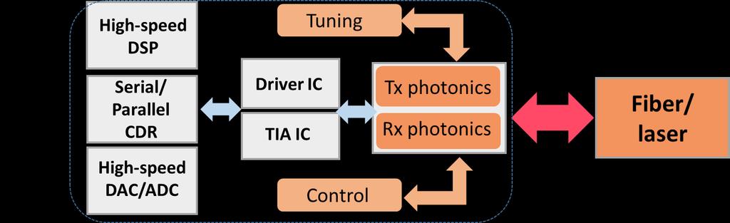
 TRANCEIVER LASER PD Transmitter MODULATOR DRIVER Receiver AMPLIFIER Fiber-uplink Fiber-downlink Major application")
12 Silicon photonic transceivers Different market segments of optical/photonic area (telecom, automotive ) Requirements for continuous growth in bandwidth and IP traffic in optical networks, Long Haul and Metro applications Goal: Join basic components of e/o Transceiver (modulator, driver, amplifier, photo-detector,..) TRANCEIVER LASER PD Transmitter MODULATOR DRIVER Receiver AMPLIFIER Fiber-uplink Fiber-downlink Major application areas for SiPh tranceivers Metro Data center 12
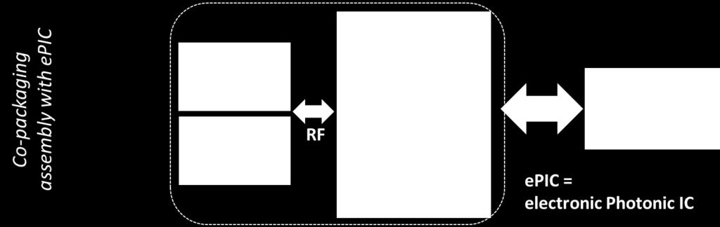
13 Transceiver is a multi-chip assembly 13


14 Major silicon epic approaches/technologies (select.) Hybrid / Co-packaging Monolithic FEOL / CMOS Photonics Monolithic FEOL / Photonic BiCMOS FEOL = Front End of Line JS Orcutt et al.; OFC 2016 Photonic SOI CMOS IHP work Zero-change Photonic CMOS. Joint: CMOS + SiGe HBT + PIC G. Denoyer et al.; JLT
 MZI modulator 130nm node passives State-of-the-art Si-photonics 40+Gb/s Strict modularity of photonic integration Re-use of parent BiCMOS devices (models) No BiCMOS yield degradation Re-use of")
15 Photonic BiCMOS 1st generation development goals 0.25µm RF-CMOS 5 ML / MIM SiGe HBTs 170GHz f T 200GHz f max 1.9V BV CEO SG25H4 BiCMOS baseline SG25H4_ePIC Ge-PDs (high bandwidth, resp.) MZI modulator 130nm node passives State-of-the-art Si-photonics 40+Gb/s Strict modularity of photonic integration Re-use of parent BiCMOS devices (models) No BiCMOS yield degradation Re-use of DigLib 15


16 Central for EPIC process integration Shared wafer Mixed Substrate: Localized SOI areas for optical structure Bulk like substrate for BiCMOS structures Common backend Modulized process flow Green: Active Red: Waveguide : STI Grey: local SOI 16
 2.")
 3.")
17 PIC- and EPIC-technology at IHP EPIC PIC 1. Mature 0.25µm-BiCMOS Technology available (SG25H4) 2. Development of PIC-process (Photonic Integrated Circuit) based on established 0.25µm-BiCMOS Technology (SG25_PIC) 3. Integration of PIC in BiCMOS EPIC (Electronic Photonic Integrated Circuit) (SG25H_EPIC) > 20 Layer > 10 Layer More than 30 Masks More than 700 process steps 17
18 EPIC Transmitters
19 Silicon cross section structuring 3 etching depths available: 220nm, 120nm, 70nm Vertical structuring is limited Freedom in horizontal structuring Dopings: p, n, p+, n+ wire waveguide Grating structures rib waveguide 19

20 Transmitters differ in phase shifter structure 4 Doped waveguide Depletion type MET3 MET2 MET1 TM1 BOX TM2 V-Pi*L [V*cm] alpha [db/cm] Voltage [V] Injection type Voltage [V] 20


21 integration Mach-Zehnder modulator segmentation Traveling wave electrode: Significant RF loss on the line Limited bandwidth and extinction ratio Velocity mismatch between optical and electrical waves Segmented MZM: Modulator divided into lumped segments Constant voltage along the phase shifter high ER Bandwidth expected to be less dependent on length longer phase shifters can be driven effectively with low driving voltage 21


22 1.3 mm Single MZM with linear driver 9.8 mm measurement ER=13.37 db 28 Gb /s simulation 1000 nm 500 nm 1640 nm 6 mm phase shifter divided into 16 segments ER=13.37 db Total fiber-to-fiber loss equal to 17 db (5 db from the phase shifter) Power dissipation equal to 2W or 71 pj/bit at 28 Gb/s EO bandwidth 18GHz D. Petousi et al, Monolithic Photonic BiCMOS Sub-System Comprising Broadband Linear Driver and Modulator Showing 13 db ER at 28 Gb/s, CLEO,


23 2 mm MZM + driver with integrated DAC Concept:. Utilizing the segmentation of the modulator Integrated DAC resolution is limited due to layout and area constraints. With digital inputs, the driver is implemented as switching amplifier reducing power dissipation light in bit 0 bit 1 bit N-1 driver w/dac + MZM light out limiting amplifiers NO EXTERNAL DAC. 9 mm D. Petousi et al. High-Speed Monolithically Integrated Silicon Photonic Transmitters in 0.25 μm BiCMOS Platform. ECOC
: ± 1s (lot): 42.34 42.34 ± 2.10 ± 2.")

24 Integrated Germanium photo diode Performance f 3dB >65GHz@-2V R>0.9A/W I dark <100nA@-1V VM2J_BW_0V M2J_BW_0V () _ () _ file: file: bias =0V, =1550nm EFA602_M2J_BW0V valid range: valid range: valid: valid: 100.0% 100.0% wafer: wafer: EFA602-[06] ± mean 1s (lot): ± 1s (lot): ± 2.10 ± 2.10 mean=42ghz ( =2GHz) dice: dice: mean ± mean 1s (wafer): ± 1s (wafer): ± 2.10 ± 2.10 Waveguide stub Metal1 contact invalid invalid > > < < Germanium photodiode building block invalid invalid class width class = width 1.00= 1.00 S. Lischke et al. Optics Express 23 (21), 2015 Jeong-Min Lee et al, Photodetection Frequency Response Characterization for High-Speed Ge-PD on Si with an Equivalent Circuit, WA2-78, OECC


25 GePD: Benchmark Responsivity, e/o BW and dark current Fully integrated Ge PD in BiCMOS exceed performance level of discrete PD Enabler for high efficient Rx EPIC designs -1 V -2 V >-2 V 25
26 EPIC Circuit Examples


27 Recent results linear SP receiver Reference PD Extended BW (36GHz) Up to 56Gbps NRZ OOK 32 Gbps 40 Gbps 28Gbd PAM4 IHP Rx 48 Gbps 56 Gbps M. Kroh et al, Monolithic Photonic-Electronic Linear Direct Detection Receiver for 56Gbps OOK, ECOC


![, OFC 2014] 2015 40 Gbps [Awny et al.](/docs-images/79/79815149/images/28-7.jpg ", MWCL 2015] 56 Gbps 2016 Grating")
28 Photonic BiCMOS evolution Demonstrators: monolithically integrated O/E RECEIVERS Gbps [Knoll et al., OFC 2014] Gbps [Awny et al., MWCL 2015] 56 Gbps 2016 Grating Coupler Ge PD TIA [ECOC2016 & ESSCIRC2016] 28


29 Photonic BiCMOS evolution Demonstrators: monolithically integrated E/O MODULATORS 10 Gbps 2013 [Zimmermann et al., ECOC 2013] HELIOS Gbps [Petousi et al., PTL 2016] 29
30 Summary Record values of f T =505 GHz, f MAX =720 GHz and t RO =1.34 ps demonstrated in an experimental SiGe HBT process Room for further improvements by lateral scaling EPIC technology developments show potential for beyond 100Gbit/s optical interfaces Ongoing challenging task of integrating these HBTs and Photonic modules in a BiCMOS platform 30
31 Acknowledgment IHP colleagues H. Rücker, B. Heinemann, D. Kissinger, H. Ng., L. Zimmermann, D. Knoll, S. Lischke, D. Petousi & M. Kroh IHP clean room staff Project partners and funding sources EU (H2020) & BMBF 31
32 Thank you for your attention! 32
Electronic-Photonic ICs for Low Cost and Scalable Datacenter Solutions
 Electronic-Photonic ICs for Low Cost and Scalable Datacenter Solutions Christoph Theiss, Director Packaging Christoph.Theiss@sicoya.com 1 SEMICON Europe 2016, October 27 2016 Sicoya Overview Spin-off from
Silicon Photonics in Optical Communications. Lars Zimmermann, IHP, Frankfurt (Oder), Germany
, Germany") Silicon Photonics in Optical Communications Lars Zimmermann, IHP, Frankfurt (Oder), Germany Outline IHP who we are Silicon photonics Photonic-electronic integration IHP photonic technology Conclusions
Silicon Photonics in Optical Communications Lars Zimmermann, IHP, Frankfurt (Oder), Germany Outline IHP who we are Silicon photonics Photonic-electronic integration IHP photonic technology Conclusions
A 3.9 ns 8.9 mw 4 4 Silicon Photonic Switch Hybrid-Integrated with CMOS Driver
 A 3.9 ns 8.9 mw 4 4 Silicon Photonic Switch Hybrid-Integrated with CMOS Driver A. Rylyakov, C. Schow, B. Lee, W. Green, J. Van Campenhout, M. Yang, F. Doany, S. Assefa, C. Jahnes, J. Kash, Y. Vlasov IBM
Silicon Photonics: an Industrial Perspective
 Silicon Photonics: an Industrial Perspective Antonio Fincato Advanced Programs R&D, Cornaredo, Italy OUTLINE 2 Introduction Silicon Photonics Concept 300mm (12 ) Photonic Process Main Silicon Photonics
Lecture: Integration of silicon photonics with electronics. Prepared by Jean-Marc FEDELI CEA-LETI
 Lecture: Integration of silicon photonics with electronics Prepared by Jean-Marc FEDELI CEA-LETI Context The goal is to give optical functionalities to electronics integrated circuit (EIC) The objectives
SiGe HBT Technology Development in the DOTSEVEN Project
 SiGe HBT Technology Development in the DOTSEVEN Project Alexander Fox 1, Bernd Heinemann 1, Josef Böck 2, Klaus Aufinger 2 1 IHP, 2 Infineon Technologies AG Open Bipolar Workshop 3 October 2013, Bordeaux
NEXT GENERATION SILICON PHOTONICS FOR COMPUTING AND COMMUNICATION PHILIPPE ABSIL
 NEXT GENERATION SILICON PHOTONICS FOR COMPUTING AND COMMUNICATION PHILIPPE ABSIL OUTLINE Introduction Platform Overview Device Library Overview What s Next? Conclusion OUTLINE Introduction Platform Overview
Silicon photonics with low loss and small polarization dependency. Timo Aalto VTT Technical Research Centre of Finland
 Silicon photonics with low loss and small polarization dependency Timo Aalto VTT Technical Research Centre of Finland EPIC workshop in Tokyo, 9 th November 2017 VTT Technical Research Center of Finland
An Example Design using the Analog Photonics Component Library. 3/21/2017 Benjamin Moss
 An Example Design using the Analog Photonics Component Library 3/21/2017 Benjamin Moss Component Library Elements Passive Library Elements: Component Current specs 1 Edge Couplers (Si)
Silicon photonics on 3 and 12 μm thick SOI for optical interconnects Timo Aalto VTT Technical Research Centre of Finland
 Silicon photonics on 3 and 12 μm thick SOI for optical interconnects Timo Aalto VTT Technical Research Centre of Finland 5th International Symposium for Optical Interconnect in Data Centres in ECOC, Gothenburg,
SiGe BiCMOS Technologies with RF and Photonic Modules
 INNOVATIONS FOR HIGH PERFORMANCE MICROELECTRONICS SiGe BiCMOS Technologies with RF and Photonic Modules Mul Project and Low Volume Wafer Produc on About Us IHP-GmbH is a German R & D institution, focused
Si Photonics Technology Platform for High Speed Optical Interconnect. Peter De Dobbelaere 9/17/2012
 Si Photonics Technology Platform for High Speed Optical Interconnect Peter De Dobbelaere 9/17/2012 ECOC 2012 - Luxtera Proprietary www.luxtera.com Overview Luxtera: Introduction Silicon Photonics: Introduction
New silicon photonics technology delivers faster data traffic in data centers
 Edition May 2017 Silicon Photonics, Photonics New silicon photonics technology delivers faster data traffic in data centers New transceiver with 10x higher bandwidth than current transceivers. Today, the
OPTICAL I/O RESEARCH PROGRAM AT IMEC
 OPTICAL I/O RESEARCH PROGRAM AT IMEC IMEC CORE CMOS PHILIPPE ABSIL, PROGRAM DIRECTOR JORIS VAN CAMPENHOUT, PROGRAM MANAGER SCALING TRENDS IN CHIP-LEVEL I/O RECENT EXAMPLES OF HIGH-BANDWIDTH I/O Graphics
Innovative ultra-broadband ubiquitous Wireless communications through terahertz transceivers ibrow
 Project Overview Innovative ultra-broadband ubiquitous Wireless communications through terahertz transceivers ibrow Mar-2017 Presentation outline Project key facts Motivation Project objectives Project
High speed silicon-based optoelectronic devices Delphine Marris-Morini Institut d Electronique Fondamentale, Université Paris Sud
 High speed silicon-based optoelectronic devices Delphine Marris-Morini Institut d Electronique Fondamentale, Université Paris Sud Data centers Optical telecommunications Environment Interconnects Silicon
New advances in silicon photonics Delphine Marris-Morini
 New advances in silicon photonics Delphine Marris-Morini P. Brindel Alcatel-Lucent Bell Lab, Nozay, France New Advances in silicon photonics D. Marris-Morini, L. Virot*, D. Perez-Galacho, X. Le Roux, D.
Millimeter-Wave Amplifiers for E- and V-band Wireless Backhaul Erik Öjefors Sivers IMA AB
 Millimeter-Wave Amplifiers for E- and V-band Wireless Backhaul Erik Öjefors Sivers IMA AB THz-Workshop: Millimeter- and Sub-Millimeter-Wave circuit design and characterization 26 September 2014, Venice
Heinrich-Hertz-Institut Berlin
 NOVEMBER 24-26, ECOLE POLYTECHNIQUE, PALAISEAU OPTICAL COUPLING OF SOI WAVEGUIDES AND III-V PHOTODETECTORS Ludwig Moerl Heinrich-Hertz-Institut Berlin Photonic Components Dept. Institute for Telecommunications,,
PLC-based integrated devices for advanced modulation formats
 ECOC 2009 workshop 7-5 Sep. 20, 2009 PLC-based integrated devices for advanced modulation formats Y. Inoue NTT Photonics Labs. NTT Corporation NTT Photonics Laboratories Hybrid integration of photonics
Nonlinear Optics in Silicon Photonics
 E-Mail: petermann@tu-berlin.de Acknowledgement TU Berlin J. Bruns, G. Dziallas, A.Gajda, M. Jazayerifar, C. Stamatiadis, K. Voigt, B. Wohlfeil IHP R. Barth, J. Drews, M. Fraschke, O. Fursenko, T. Grabolla,
Silicon-Organic hybrid Fabrication platform for Integrated circuits FP7-ICT GA No
 www.sofi-ict.eu FP7-ICT-2009.3.8 GA No. 248609 Participants: 2 Outline Today s High Speed Interconnects Vision : Convergence of Photonics & Electronics Silicon Photonics Technology Silicon-Organic Hybrid
Si and InP Integration in the HELIOS project
 Si and InP Integration in the HELIOS project J.M. Fedeli CEA-LETI, Grenoble ( France) ECOC 2009 1 Basic information about HELIOS HELIOS photonics ELectronics functional Integration on CMOS www.helios-project.eu
Silicon Photonics Technology Platform To Advance The Development Of Optical Interconnects
 Silicon Photonics Technology Platform To Advance The Development Of Optical Interconnects By Mieke Van Bavel, science editor, imec, Belgium; Joris Van Campenhout, imec, Belgium; Wim Bogaerts, imec s associated
Silicon Avalanche Photodetectors Fabricated With Standard CMOS/BiCMOS Technology Myung-Jae Lee
 Silicon Avalanche Photodetectors Fabricated With Standard CMOS/BiCMOS Technology Myung-Jae Lee The Graduate School Yonsei University Department of Electrical and Electronic Engineering Silicon Avalanche
Silicon Photonics Opportunity, applications & Recent Results
 Silicon Photonics Opportunity, applications & Recent Results Dr. Mario Paniccia Intel Fellow Director, Photonics Technology Lab Intel Corporation www.intel.com/go/sp Purdue University Oct 5 2007 Agenda
VERSATILE SILICON PHOTONIC PLATFORM FOR DATACOM AND COMPUTERCOM APPLICATIONS. B Szelag CEA-Leti
 VERSATILE SILICON PHOTONIC PLATFORM FOR DATACOM AND COMPUTERCOM APPLICATIONS B Szelag CEA-Leti OUTLINE Silicon photonic : 200mm CMOS core technology towards 300mm Emergent needs vs core process Technological
WWDM Transceiver Module for 10-Gb/s Ethernet
 WWDM Transceiver Module for 10-Gb/s Ethernet Brian E. Lemoff Hewlett-Packard Laboratories lemoff@hpl.hp.com IEEE 802.3 HSSG Interim Meeting Coeur d Alene, Idaho June 1-3, 1999 Why pursue WWDM for the LAN?
EE 232 Lightwave Devices Optical Interconnects
 EE 232 Lightwave Devices Optical Interconnects Sajjad Moazeni Department of Electrical Engineering & Computer Sciences University of California, Berkeley 1 Emergence of Optical Links US IT Map Hyper-Scale
Opportunities and challenges of silicon photonics based System-In-Package
 Opportunities and challenges of silicon photonics based System-In-Package ECTC 2014 Panel session : Emerging Technologies and Market Trends of Silicon Photonics Speaker : Stéphane Bernabé (Leti Photonics
Integration of Optoelectronic and RF Devices for Applications in Optical Interconnect and Wireless Communication
 Integration of Optoelectronic and RF Devices for Applications in Optical Interconnect and Wireless Communication Zhaoran (Rena) Huang Assistant Professor Department of Electrical, Computer and System Engineering
Silicon Photonics Transceivers for Hyper Scale Datacenters: Deployment and Roadmap
 Silicon Photonics Transceivers for Hyper Scale Datacenters: Deployment and Roadmap Peter De Dobbelaere Luxtera Inc. 09/19/2016 Luxtera Proprietary www.luxtera.com Luxtera Company Introduction $100B+ Shift
Silicon Photonics: A Platform for Integration, Wafer Level Assembly and Packaging
 Silicon Photonics: A Platform for Integration, Wafer Level Assembly and Packaging M. Asghari Kotura Inc April 27 Contents: Who is Kotura Choice of waveguide technology Challenges and merits of Si photonics
Innovations in Photonic Integration Platforms
 Innovations in Photonic Integration Platforms September 20, 20 Burgeoning Growth Demand Disruptive Technology Video content is fast becoming a larger percentage of total internet traffic 50% Video services
From 1 Tbs per Carrier to 1 THz
 From 1 Tbs per Carrier to 1 THz Sorin P. Voinigescu ECE Department, University of Toronto European Microwave Conference 1 Outline Introduction Examples of Tbs Wireless and Photonics Systems Segmented Power
A silicon avalanche photodetector fabricated with standard CMOS technology with over 1 THz gain-bandwidth product
 A silicon avalanche photodetector fabricated with standard CMOS technology with over 1 THz gain-bandwidth product Myung-Jae Lee and Woo-Young Choi* Department of Electrical and Electronic Engineering,
The Past, Present, and Future of Silicon Photonics
 The Past, Present, and Future of Silicon Photonics Myung-Jae Lee High-Speed Circuits & Systems Lab. Dept. of Electrical and Electronic Engineering Yonsei University Outline Introduction A glance at history
Overview of technology for RF and Digital Optical Communications
 Overview of technology for RF and Digital Optical Communications Structure of talk Day 1 Introduction What is EPIC, How has EPIC evolved Use to show how a research and development capability matched to
Si photonics for the Zettabyte Era. Marco Romagnoli. CNIT & TeCIP - Scuola Superiore Sant Anna
 Si photonics for the Zettabyte Era Marco Romagnoli CNIT & TeCIP - Scuola Superiore Sant Anna Semicon 2013 Dresden 8-10 October 2013 Zetabyte era Disaggregation at system level Integration at chip level
APSUNY PDK: Overview and Future Trends
 APSUNY PDK: Overview and Future Trends Erman Timurdogan Analog Photonics, 1 Marina Park Drive, Suite 205, Boston, MA, 02210 erman@analogphotonics.com Silicon Photonics Integrated Circuit Process Design
A Fully Integrated 20 Gb/s Optoelectronic Transceiver Implemented in a Standard
 A Fully Integrated 20 Gb/s Optoelectronic Transceiver Implemented in a Standard 0.13 µm CMOS SOI Technology School of Electrical and Electronic Engineering Yonsei University 이슬아 1. Introduction 2. Architecture
Emerging Highly Compact Amplification Solutions for Coherent Transmission
 Emerging Highly Compact Amplification Solutions for Coherent Transmission Market Focus ECOC 2017 Sep 20, 2017 Dr. Sanjai Parthasarathi Vice President, Product Marketing & Strategy II-VI Photonics Outline
PROJECT FINAL REPORT
 PROJECT FINAL REPORT Grant Agreement number: FP7-224312 Project acronym: HELIOS Project title: photonics ELectronics functional Integration on CMOS Funding Scheme: Large Scale Integrating Project Period
Si CMOS Technical Working Group
 Si CMOS Technical Working Group CTR, Spring 2008 meeting Markets Interconnects TWG Breakouts Reception TWG reports Si CMOS: photonic integration E-P synergy - Integration - Standardization - Cross-market
SNR characteristics of 850-nm OEIC receiver with a silicon avalanche photodetector
 SNR characteristics of 850-nm OEIC receiver with a silicon avalanche photodetector Jin-Sung Youn, 1 Myung-Jae Lee, 1 Kang-Yeob Park, 1 Holger Rücker, 2 and Woo-Young Choi 1,* 1 Department of Electrical
Silicon Photonics Photo-Detector Announcement. Mario Paniccia Intel Fellow Director, Photonics Technology Lab
 Silicon Photonics Photo-Detector Announcement Mario Paniccia Intel Fellow Director, Photonics Technology Lab Agenda Intel s Silicon Photonics Research 40G Modulator Recap 40G Photodetector Announcement
Project: IEEE P Working Group for Wireless Personal Area Networks (WPANs)
") Project: IEEE P802.15 Working Group for Wireless Personal Area Networks (WPANs) Title: Feasibility test of THz channel for high-speed wireless link Date Submitted: 12 Nov 2013 Source: Jae-Young Kim, Ho-Jin
Project: IEEE P802.15 Working Group for Wireless Personal Area Networks (WPANs) Title: Feasibility test of THz channel for high-speed wireless link Date Submitted: 12 Nov 2013 Source: Jae-Young Kim, Ho-Jin
An Inductor-Based 52-GHz 0.18 µm SiGe HBT Cascode LNA with 22 db Gain
 An Inductor-Based 52-GHz 0.18 µm SiGe HBT Cascode LNA with 22 db Gain Michael Gordon, Sorin P. Voinigescu University of Toronto Toronto, Ontario, Canada ESSCIRC 2004, Leuven, Belgium Outline Motivation
New Wave SiP solution for Power
 New Wave SiP solution for Power Vincent Lin Corporate R&D ASE Group APEC March 7 th, 2018 in San Antonio, Texas. 0 Outline Challenges Facing Human Society Energy, Environment and Traffic Autonomous Driving
What to do with THz? Ali M. Niknejad Berkeley Wireless Research Center University of California Berkeley. WCA Futures SIG
 What to do with THz? Ali M. Niknejad Berkeley Wireless Research Center University of California Berkeley WCA Futures SIG Outline THz Overview Potential THz Applications THz Transceivers in Silicon? Application
Envisioning the Future of Optoelectronic Interconnects:
 Envisioning the Future of Optoelectronic Interconnects: The Production Economics of InP and Si Platforms for 100G Ethernet LAN Transceivers Shan Liu Dr. Erica Fuchs Prof. Randolph Kirchain MIT Microphotonics
Silicon Carrier-Depletion-Based Mach-Zehnder and Ring Modulators with Different Doping Patterns for Telecommunication and Optical Interconnect
 Silicon Carrier-Depletion-Based Mach-Zehnder and Ring Modulators with Different Doping Patterns for Telecommunication and Optical Interconnect Hui Yu, Marianna Pantouvaki*, Joris Van Campenhout*, Katarzyna
Packaged mm-wave GaN, GaAs and Si ICs for 5G and automotive radar
 Packaged mm-wave GaN, GaAs and Si ICs for 5G and automotive radar Eric Leclerc UMS 1 st Nov 2018 Outline Why heterogenous integration? About UMS Technology portfolio Design tooling: Cadence / GoldenGate
Low Power DSP and Photonic Integration in Optical Networks. Atul Srivastava CTO, NTT Electronics - America. Market Focus ECOC 2014
 Low Power DSP and Photonic Integration in Optical Networks Atul Srivastava CTO, NTT Electronics - America Market Focus ECOC 2014 Outline 100G Deployment Rapid Growth in Long Haul Role of Modules New Low
High-speed Ge photodetector monolithically integrated with large cross silicon-on-insulator waveguide
 [ APPLIED PHYSICS LETTERS ] High-speed Ge photodetector monolithically integrated with large cross silicon-on-insulator waveguide Dazeng Feng, Shirong Liao, Roshanak Shafiiha. etc Contents 1. Introduction
High-Speed Optical Modulators and Photonic Sideband Management
 114 High-Speed Optical Modulators and Photonic Sideband Management Tetsuya Kawanishi National Institute of Information and Communications Technology 4-2-1 Nukui-Kita, Koganei, Tokyo, Japan Tel: 81-42-327-7490;
Optoelectronic Components Testing with a VNA(Vector Network Analyzer) VNA Roadshow Budapest 17/05/2016
 VNA Roadshow Budapest 17/05/2016") Optoelectronic Components Testing with a VNA(Vector Network Analyzer) VNA Roadshow Budapest 17/05/2016 Content Introduction Photonics & Optoelectronics components Optical Measurements VNA (Vector Network
Optoelectronic Components Testing with a VNA(Vector Network Analyzer) VNA Roadshow Budapest 17/05/2016 Content Introduction Photonics & Optoelectronics components Optical Measurements VNA (Vector Network
High Speed Detectors. Andreas Umbach ECOC 2009, Workshop 7 Monolithic and Hybrid Photonic Integrated Transceivers for Advanced Modulation Formats
 High Speed Detectors Andreas Umbach ECOC 2009, Workshop 7 Monolithic and Hybrid Photonic Integrated Transceivers for Advanced Modulation Formats 100 Gbit/s Long-Haul Transport Optical networks use "standardized"
Photonic Integrated Circuits Made in Berlin
 Fraunhofer Heinrich Hertz Institute Photonic Integrated Circuits Made in Berlin Photonic integration Workshop, Columbia University, NYC October 2015 Moritz Baier, Francisco M. Soares, Norbert Grote Fraunhofer
IBM T. J. Watson Research Center IBM Corporation
 Broadband Silicon Photonic Switch Integrated with CMOS Drive Electronics B. G. Lee, J. Van Campenhout, A. V. Rylyakov, C. L. Schow, W. M. J. Green, S. Assefa, M. Yang, F. E. Doany, C. V. Jahnes, R. A.
Silicon-On-Insulator based guided wave optical clock distribution
 Silicon-On-Insulator based guided wave optical clock distribution K. E. Moselund, P. Dainesi, and A. M. Ionescu Electronics Laboratory Swiss Federal Institute of Technology People and funding EPFL Project
Convergence Challenges of Photonics with Electronics
 Convergence Challenges of Photonics with Electronics Edward Palen, Ph.D., P.E. PalenSolutions - Optoelectronic Packaging Consulting www.palensolutions.com palensolutions@earthlink.net 415-850-8166 October
EPIC: The Convergence of Electronics & Photonics
 EPIC: The Convergence of Electronics & Photonics K-Y Tu, Y.K. Chen, D.M. Gill, M. Rasras, S.S. Patel, A.E. White ell Laboratories, Lucent Technologies M. Grove, D.C. Carothers, A.T. Pomerene, T. Conway
Index. Cambridge University Press Silicon Photonics Design Lukas Chrostowski and Michael Hochberg. Index.
 absorption, 69 active tuning, 234 alignment, 394 396 apodization, 164 applications, 7 automated optical probe station, 389 397 avalanche detector, 268 back reflection, 164 band structures, 30 bandwidth
High speed electronics (in optical communications)
") High speed electronics (in optical communications) SOK-2013 Conference January 30/31, February 1, 2013 Ljubljana Franz Dielacher Marc Tiebout, Rudolf Lachner, Klaus Aufinger, Herbert Knapp, Koen Mertens,
High speed electronics (in optical communications) SOK-2013 Conference January 30/31, February 1, 2013 Ljubljana Franz Dielacher Marc Tiebout, Rudolf Lachner, Klaus Aufinger, Herbert Knapp, Koen Mertens,
THz communications: general issues THz devices for coms (Tx and Rx) Some Reported com links Some conclusions
 Some Reported com links Some conclusions") THz communications for next generation HD rate wireless links TENXSYS Talk, 2015, June 17th G. Ducournau, M. Zaknoune, P. Szriftgiser, Jean-François Lampin (Tx and Rx) (Tx and Rx) 2 3 THz coms: general
THz communications for next generation HD rate wireless links TENXSYS Talk, 2015, June 17th G. Ducournau, M. Zaknoune, P. Szriftgiser, Jean-François Lampin (Tx and Rx) (Tx and Rx) 2 3 THz coms: general
IEEE JOURNAL OF SELECTED TOPICS IN QUANTUM ELECTRONICS 2010 Silicon Photonic Circuits: On-CMOS Integration, Fiber Optical Coupling, and Packaging
 IEEE JOURNAL OF SELECTED TOPICS IN QUANTUM ELECTRONICS 2010 Silicon Photonic Circuits: On-CMOS Integration, Fiber Optical Coupling, and Packaging Christophe Kopp, St ephane Bernab e, Badhise Ben Bakir,
Integrated Photonics using the POET Optical InterposerTM Platform
 Integrated Photonics using the POET Optical InterposerTM Platform Dr. Suresh Venkatesan CIOE Conference Shenzhen, China Sept. 5, 2018 POET Technologies Inc. TSXV: PUBLIC POET PTK.V Technologies Inc. PUBLIC
Indium Phosphide and Related Materials Selectively implanted subcollector DHBTs
 Indium Phosphide and Related Materials - 2006 Selectively implanted subcollector DHBTs Navin Parthasarathy, Z. Griffith, C. Kadow, U. Singisetti, and M.J.W. Rodwell Dept. of Electrical and Computer Engineering,
Optical Interconnection in Silicon LSI
 The Fifth Workshop on Nanoelectronics for Tera-bit Information Processing, 1 st Century COE, Hiroshima University Optical Interconnection in Silicon LSI Shin Yokoyama, Yuichiro Tanushi, and Masato Suzuki
Silicon Photonics : Towards Heterogeneous and Multi-layer Integration for High Density Circuits
 Silicon Photonics : Towards Heterogeneous and Multi-layer Integration for High Density Circuits Stéphane Bernabé, Ségolène Olivier, Bertrand Szelag, Daivid Fowler, Christophe Kopp OPTICS, Dresden, 23-03-16
Putting PICs in Products A Practical Guideline. Katarzyna Ławniczuk
 Putting PICs in Products A Practical Guideline Katarzyna Ławniczuk k.lawniczuk@brightphotonics.eu Outline Product development considerations Selecting PIC technology Design flow and design tooling considerations
Fiber-fed wireless systems based on remote up-conversion techniques
 2008 Radio and Wireless Symposium incorporating WAMICON 22 24 January 2008, Orlando, FL. Fiber-fed wireless systems based on remote up-conversion techniques Jae-Young Kim and Woo-Young Choi Dept. of Electrical
A Millimeter-Wave Power Amplifier Concept in SiGe BiCMOS Technology for Investigating HBT Physical Limitations
 A Millimeter-Wave Power Amplifier Concept in SiGe BiCMOS Technology for Investigating HBT Physical Limitations Jonas Wursthorn, Herbert Knapp, Bernhard Wicht Abstract A millimeter-wave power amplifier
SUPPLEMENTARY INFORMATION
 In the format provided by the authors and unedited. DOI: 10.1038/NPHOTON.2016.233 A monolithic integrated photonic microwave filter Javier S. Fandiño 1, Pascual Muñoz 1,2, David Doménech 2 & José Capmany
Updates on THz Amplifiers and Transceiver Architecture
 Updates on THz Amplifiers and Transceiver Architecture Sanggeun Jeon, Young-Chai Ko, Moonil Kim, Jae-Sung Rieh, Jun Heo, Sangheon Pack, and Chulhee Kang School of Electrical Engineering Korea University
50-Gb/s silicon optical modulator with travelingwave
 5-Gb/s silicon optical modulator with travelingwave electrodes Xiaoguang Tu, 1, * Tsung-Yang Liow, 1 Junfeng Song, 1,2 Xianshu Luo, 1 Qing Fang, 1 Mingbin Yu, 1 and Guo-Qiang Lo 1 1 Institute of Microelectronics,
A 24-Channel 300 Gb/s 8.2 pj/bit Full-Duplex Fiber-Coupled Optical Transceiver Module Based on a Single Holey CMOS IC
 A 24-Channel 300 Gb/s 8.2 pj/bit Full-Duplex Fiber-Coupled Optical Transceiver Module Based on a Single Holey CMOS IC A. Rylyakov, C. Schow, F. Doany, B. Lee, C. Jahnes, Y. Kwark, C.Baks, D. Kuchta, J.
UNIVERSITY OF TORONTO FACULTY OF APPLIED SCIENCE AND ENGINEERING. FINAL EXAMINATION, April 2017 DURATION: 2.5 hours
 UNIVERSITY OF TORONTO FACULTY OF APPLIED SCIENCE AND ENGINEERING ECE4691-111 S - FINAL EXAMINATION, April 2017 DURATION: 2.5 hours Optical Communication and Networks Calculator Type: 2 Exam Type: X Examiner:
- no emitters/amplifiers available. - complex process - no CMOS-compatible
 Advantages of photonic integrated circuits (PICs) in Microwave Photonics (MWP): compactness low-power consumption, stability flexibility possibility of aggregating optics and electronics functionalities
Light source approach for silicon photonics transceivers September Fiber to the Chip
 Light source approach for silicon photonics transceivers September 2014 Fiber to the Chip Silicon Photonics Silicon Photonics Technology: Silicon material system & processing techniques to manufacture
Monolithic Integra/on of O-band Photonic Transceivers in a Zero-change 32nm SOI CMOS
 Monolithic Integra/on of O-band Photonic Transceivers in a Zero-change 32nm SOI CMOS S. Moazeni 1, A. Atabaki 2, D. Cheian 2, S. Lin 1, R. J. Ram 2, and V. Stojanović 1 1 Department of EECS, University
A HIGH SPEED WDM PON FOR DOWNSTREAM DPSK ASK SIGNALS AND UPSTREAM OOK SIGNAL WITH BROADCAST CAPABILTY
 A HIGH SPEED WDM PON FOR DOWNSTREAM DPSK ASK SIGNALS AND UPSTREAM OOK SIGNAL WITH BROADCAST CAPABILTY 1 AAMIR KHAN, 2 ANITA CHOPRA 1 Department of Information Technology, Suresh Gyan Vihar University,
Introduction to ixblue RF drivers and amplifiers for optical modulators
 Introduction to ixblue RF drivers and amplifiers for optical modulators Introduction : ixblue designs, produces and commercializes optical modulators intended for a variety of applications including :
Heterogeneously Integrated Microwave Signal Generators with Narrow- Linewidth Lasers
 Heterogeneously Integrated Microwave Signal Generators with Narrow- Linewidth Lasers John E. Bowers, Jared Hulme, Tin Komljenovic, Mike Davenport and Chong Zhang Department of Electrical and Computer Engineering
A CMOS-compatible silicon photonic platform for high-speed integrated opto-electronics
 Invited Paper A CMOS-compatible silicon photonic platform for high-speed integrated opto-electronics Christophe Galland 1, Ari Novack 3,4, Yang Liu 1, Ran Ding 1, Michael Gould 2, Tom Baehr-Jones 1, Qi
Dual Parallel Mach-Zehnder (DPMZ) Modulator
 Modulator") AGILE OPTICAL COMPONENTS Dual Parallel Mach-Zehnder (DPMZ) Modulator Key Features Monolithically integrated, parallel, high-speed MZ modulators, with a phase modulator superstructure High-speed MZ modulators
AGILE OPTICAL COMPONENTS Dual Parallel Mach-Zehnder (DPMZ) Modulator Key Features Monolithically integrated, parallel, high-speed MZ modulators, with a phase modulator superstructure High-speed MZ modulators
ECEN689: Special Topics in Optical Interconnects Circuits and Systems Spring 2016
 ECEN689: Special Topics in Optical Interconnects Circuits and Systems Spring 2016 Lecture 1: Introduction Sam Palermo Analog & Mixed-Signal Center Texas A&M University Class Topics System and design issues
Photonics Integration and Evolution of the Optical Transceiver Presented by: Giacomo Losio ProLabs
 Photonics Integration and Evolution of the Optical Transceiver Presented by: Giacomo Losio ProLabs Optical Transceivers architecture is challenged Electrical Driver TIA Laser Photodiode Optical Optical
Project Overview. Innovative ultra-broadband ubiquitous Wireless communications through terahertz transceivers ibrow
 Project Overview Innovative ultra-broadband ubiquitous Wireless communications through terahertz transceivers ibrow Presentation outline Key facts Consortium Motivation Project objective Project description
Quantum-effect Resonant Tunneling Device Technology for Practical Ultra Low-power High-speed Applications
 Quantum-effect Resonant Tunneling Device Technology for Practical Ultra Low-power High-speed Applications SEMATECH Symposium October 23 rd, 2012 Prof. Kyounghoon Yang High Speed Nanoelectronics Laboratory
Photonic Integrated Circuit for Radio-Frequency Interference Cancellation
 Developing a Photonic Integrated Circuit for Radio-Frequency Interference Cancellation Matthew Chang, Monica Lu, Jenny Sun and Paul R. Prucnal Lightwave Communications Research Lab Princeton University
ECEN689: Special Topics in Optical Interconnects Circuits and Systems Spring 2016
 ECEN689: Special Topics in Optical Interconnects Circuits and Systems Spring 2016 Lecture 9: Mach-Zehnder Modulator Transmitters Sam Palermo Analog & Mixed-Signal Center Texas A&M University Mach-Zehnder
Senior Project Manager / Keysight Joe Lin 林昭彥
 Senior Project Manager / Keysight 2017.04.17 Joe Lin 林昭彥 How do you build a 400G optical link? Multimode fiber or single-mode fiber? IEEE 802.3bs 400G will use both multimode fiber for 100 meter spans
A 30-GS/sec Track and Hold Amplifier in 0.13-µm CMOS Technology Shahriar Shahramian Sorin P. Voinigescu Anthony Chan Carusone
 A 30-GS/sec Track and Hold Amplifier in 0.13-µm CMOS Technology Shahriar Shahramian Sorin P. Voinigescu Anthony Chan Carusone Department of Electrical & Computer Eng. University of Toronto Canada Introduction
ECEN689: Special Topics in Optical Interconnects Circuits and Systems Spring 2016
 ECEN689: Special Topics in Optical Interconnects Circuits and Systems Spring 2016 Lecture 10: Electroabsorption Modulator Transmitters Sam Palermo Analog & Mixed-Signal Center Texas A&M University Announcements
Trends in Optical Transceivers:
 Trends in Optical Transceivers: Light sources for premises networks Peter Ronco Corning Optical Fiber Asst. Product Line Manager Premises Fibers January 24, 2006 Outline: Introduction: Transceivers and
SEVENTH FRAMEWORK PROGRAMME THEME [ICT ] [Photonics]
![SEVENTH FRAMEWORK PROGRAMME THEME [ICT ] [Photonics]](/thumbs/91/106870333.jpg "SEVENTH FRAMEWORK PROGRAMME THEME [ICT ] [Photonics]") SEVENTH FRAMEWORK PROGRAMME THEME [ICT-2013.3.2] [Photonics] Software-defined energy-efficient Photonic transceivers IntRoducing Intelligence and dynamicity in Terabit superchannels for flexible optical
SEVENTH FRAMEWORK PROGRAMME THEME [ICT-2013.3.2] [Photonics] Software-defined energy-efficient Photonic transceivers IntRoducing Intelligence and dynamicity in Terabit superchannels for flexible optical
High-Frequency Transistors High-Frequency ICs. Technologies & Applications
 High-Frequency Transistors High-Frequency ICs Technologies & Applications Mark Rodwell University of California, Santa Barbara rodwell@ece.ucsb.edu 805-893-3244, 805-893-2362 fax Report Documentation Page
Silicon Optical Modulator
 Silicon Optical Modulator Silicon Optical Photonics Nature Photonics Published online: 30 July 2010 Byung-Min Yu 24 April 2014 High-Speed Circuits & Systems Lab. Dept. of Electrical and Electronic Engineering