Si photonics for the Zettabyte Era. Marco Romagnoli. CNIT & TeCIP - Scuola Superiore Sant Anna
|
|
|
- Jacob Sullivan
- 6 years ago
- Views:
Transcription


1 Si photonics for the Zettabyte Era Marco Romagnoli CNIT & TeCIP - Scuola Superiore Sant Anna Semicon 2013 Dresden 8-10 October 2013
2 Zetabyte era Disaggregation at system level Integration at chip level Optical interconnection at shorter reach Electronics-photonics convergence Cost, energy and bandwidth density Architecture, components, SW programming Make it happen or end the information age
3 Example of applications Active Optical Cable Wireless communications 100GE Optical Interfaces (CFP, CXP, CPAK, QFSP,..) Optical switching Inter Chip and Board Level Interconnection

4 Thunderbolt, new version based on optical cable up to 30m long Sumitomo Electric Industries have been certified by Intel for manufacturing AOC s 10, 20, and 30 mts long. This allows high speed and possibility of connection over distances greater than 1 mt Interestingly a blue ray download at 10 Gb/s occurs in 30 s, at 100Gb/s this would happen in 3 s! Si Photonics could be the technology that allows 100G interconnection at the cost of actual 10G AOC s. In principle 100G at same cost is feasible in the next future


.")

5 Silicon photonic use in products in near term Si photonics for optical interconnection Radio Base Station and Router: low cost, low power, high capacity, reduced footprint and cabling, very large volumes Key devices: Up to 10 km long links, 10 Gb/s parallel optics transceivers for high density intra-system interconnect (DU-RRU in RBS and inter-rack connection in Routers). CPRI (for RBS fronthaul) and Ethernet signals will be supported Next: 4x25 Gbps transceivers, parallel optics or WDM, for intra-system interconnect as evolution of the 10 Gbps to scale up the capacity.

6 Optical Interfaces for Different Network Platforms Datacom (CXP, CPAK) Telecom (CFP) Data center access Data center aggregation Edge routing Core routing The Optical challenges: Bandwidth Density Cost Consumption
 multiplies the number of 100 Gb/s optical module interfaces on a blade.")

7 The CFP (C Form-Factor Pluggable) optical module to enable Terabit blades or line-cards The next-generation CFP modules - the CFP2 and CFP4 (10/40 km) multiplies the number of 100 Gb/s optical module interfaces on a blade. Using the CFP4, up to 16, 100Gbps modules will fit on a blade, a total line rate of 1.6 Tb/s. With a goal of a 60W total module power budget per blade, that equates to 27Gb/s/W. In comparison, the power-efficient SFP+ achieves 10Gbps/W.

 Cost: low Footprint: miniaturized T T T Mini-")
8 T T T T T T Optical switching for Add Drop Multiplexing Field of application: lightpath reconfiguration in Metro-access and Access network (e.g. mobile backhaul) Cost: low Footprint: miniaturized T T T Mini- ROADM Mini- ROADM Mini- ROADM Mini- ROADM T T T


 of the")
9 Inter Chip and Board Level Interconnection Case study: «Optical PCIe3.0» working group within the Communication Technology Roadmap (CTR4) of the Microphotonics Center Consortium (MPhC) at MIT

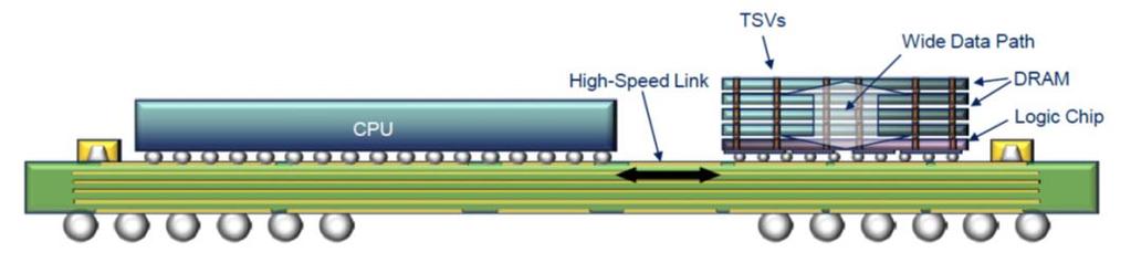
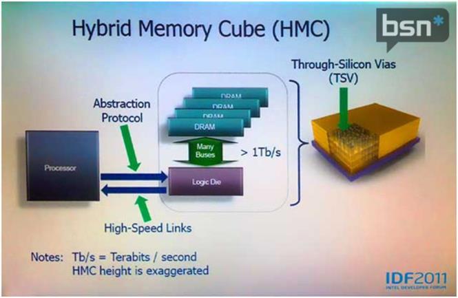

10 Chip to Memory Interconnection Interconnection through Si interposer
11 Technology
.")
12 Electrical Interconnect Limitations Bandwidth Limitations Wires are not scalable. Bandwidth is fundamentally limited by the available area Power Limitations - Total interconnect power is high ~50% of Total Chip Power Expected to rise to >80% (limit 200W). Signal Integrity and Latency Limitations RC Delay will increase considerably with scaling Al/Oxide + Gates Al/Oxide Sam Naftziger, AMD fellow 2011 VLSI Symposium Keynote Cu + Gate Cu Gate
13 Photonic Electronic Layer - 3D Integration 3D integration of SOI technology for the photonic layers with Si CMOS technology for the circuit layers. Integration in a 65nm node/12 fab based on wf/wf or wf/die bonding and low capacitance TSV technology. Bond Pads Si Logic Layer TSV Si TSV Thermal Compression Bonding SOI Photonics Layer PD Mod Si waveguide Substrate 13

14 Si Interposer Si Interposer Si Optical Interposer Coupler Micro Bumps Silica Waveguides Heat Sink 100nP m + Photonic Electronic Layer Metal Pad / via 480n 220n m P N m N + N + MZI Modulat or Oxide N Micro Bumps P Si Substrate P + BOX P G e N+ Silicon + Waveguide Ge Photodetect or Silicon Waveguides, resonators, detectors 1.5um Optical Fiber I/O HMC ASIC HMC Interposer Package Redistribution layer Flip Chip Bumps BGA Balls Interpose / Photonics Layer TSV Redistribution Layer
.")


15 Si Photonics - Advantage of full integration Cost: photonic-electronic chip (development, mask set, wafers, manufacturing). Save in packaging, wire bonding and traces/pin-out. Technology: low capacitance 3D integration. Node scalability, low consumption and improved yield. Performances: trade off between consumption, size, IL and link/system specs Maturity of individual components: to be improved but not conceptually limited. Photonic chip 15
16 Si Photonics Full integration: Integrated Laser Source Hybrid mounting III-V: conventional solution. It can be butt coupled or coupled through grating coupler. Coupling loss 1 3dB, TEC, Packaging, assembly. Cost and large consumption. Uncooled is preferred. VCSEL: conventional solution for <100m reach. Good for power consumption, temperature stability, packaging and cost. Drawback: MM interconnection Single mode VCSEL are now becoming available. Bonded III-V Laser: remarkable solution at initial stage of R&D. Industrialization to be demonstrated. Threshold current and reliability to be improved. Ge Laser: The only monolithic solution. Potential good performance (power and threshold). Large gain BW and wide tunability. Best operation at high T ( C). To be developed. 16


17 Aurrion Hybrid Silicon Platform bonds III/V wafer or die to silicon. 150-mm wafer bonding and processing possible; III/V processed in low-temperature backend process; Mode couples to III/V optical gain, detection or modulation from III-V Material. Fujitsu Hybrid III/V SOA mounted on Si Platforrm; Mode butt couples to III/V optical gain Fujitsu
18
19 Technological challenges Parameters to be improved Link loss budget Laser consumption Laser cooling Laser operating temperature Thermal impedance Cost Targets Medium/short reach 100G Ethernet 100GE LR4 & SR4: CFP4 and QFSP 400GE nr16 & SR16: CFP4x4 I/O: 16x 25G (CDAUI, NRZ) CFP2 I/O: 8x 50G (CDAUI-8, PAM-4 or NRZ) RBS-DU 10G up to 10km Others Short reach Multi Chip Module Bandwidth scalability Bandwidth density/area (e.g. 30Tbps/cm 2 )
20 Conclusions Assuming Maturity of Si Photonics low consumption, good performance, component availability Early stage of photonics electronics integration Needs Low consumption, uncooled operation laser integration evolution Photonic Electronic convergence through Si optical interposer (3D integration, TSV s interconnections) Result Huge energy saving Latency control Increase of BW density Miniaturization Lower costs Zetabyte Era


21 thank you!
Opportunities and challenges of silicon photonics based System-In-Package
 Opportunities and challenges of silicon photonics based System-In-Package ECTC 2014 Panel session : Emerging Technologies and Market Trends of Silicon Photonics Speaker : Stéphane Bernabé (Leti Photonics
Silicon Photonics Transceivers for Hyper Scale Datacenters: Deployment and Roadmap
 Silicon Photonics Transceivers for Hyper Scale Datacenters: Deployment and Roadmap Peter De Dobbelaere Luxtera Inc. 09/19/2016 Luxtera Proprietary www.luxtera.com Luxtera Company Introduction $100B+ Shift
NEXT GENERATION SILICON PHOTONICS FOR COMPUTING AND COMMUNICATION PHILIPPE ABSIL
 NEXT GENERATION SILICON PHOTONICS FOR COMPUTING AND COMMUNICATION PHILIPPE ABSIL OUTLINE Introduction Platform Overview Device Library Overview What s Next? Conclusion OUTLINE Introduction Platform Overview
Si Photonics Technology Platform for High Speed Optical Interconnect. Peter De Dobbelaere 9/17/2012
 Si Photonics Technology Platform for High Speed Optical Interconnect Peter De Dobbelaere 9/17/2012 ECOC 2012 - Luxtera Proprietary www.luxtera.com Overview Luxtera: Introduction Silicon Photonics: Introduction
Convergence Challenges of Photonics with Electronics
 Convergence Challenges of Photonics with Electronics Edward Palen, Ph.D., P.E. PalenSolutions - Optoelectronic Packaging Consulting www.palensolutions.com palensolutions@earthlink.net 415-850-8166 October
Integrated Photonics using the POET Optical InterposerTM Platform
 Integrated Photonics using the POET Optical InterposerTM Platform Dr. Suresh Venkatesan CIOE Conference Shenzhen, China Sept. 5, 2018 POET Technologies Inc. TSXV: PUBLIC POET PTK.V Technologies Inc. PUBLIC
Lecture: Integration of silicon photonics with electronics. Prepared by Jean-Marc FEDELI CEA-LETI
 Lecture: Integration of silicon photonics with electronics Prepared by Jean-Marc FEDELI CEA-LETI Context The goal is to give optical functionalities to electronics integrated circuit (EIC) The objectives
Silicon Photonics for Mid-Board Optical Modules Marc Epitaux
 Silicon Photonics for Mid-Board Optical Modules Marc Epitaux Chief Architect at Samtec, Inc Outline Interconnect Solutions Mid-Board Optical Modules Silicon Photonics o Benefits o Challenges DragonFly
Silicon Photonics Photo-Detector Announcement. Mario Paniccia Intel Fellow Director, Photonics Technology Lab
 Silicon Photonics Photo-Detector Announcement Mario Paniccia Intel Fellow Director, Photonics Technology Lab Agenda Intel s Silicon Photonics Research 40G Modulator Recap 40G Photodetector Announcement
Chip Scale Package Fiber Optic Transceiver Integration for Harsh Environments
 Chip Scale Package Fiber Optic Transceiver Integration for Harsh Environments Chuck Tabbert and Charlie Kuznia Ultra Communications, Inc. 990 Park Center Drive, Suite H Vista, CA, USA, 92081 ctabbert@
Si CMOS Technical Working Group
 Si CMOS Technical Working Group CTR, Spring 2008 meeting Markets Interconnects TWG Breakouts Reception TWG reports Si CMOS: photonic integration E-P synergy - Integration - Standardization - Cross-market
Emerging Highly Compact Amplification Solutions for Coherent Transmission
 Emerging Highly Compact Amplification Solutions for Coherent Transmission Market Focus ECOC 2017 Sep 20, 2017 Dr. Sanjai Parthasarathi Vice President, Product Marketing & Strategy II-VI Photonics Outline
OPTICAL I/O RESEARCH PROGRAM AT IMEC
 OPTICAL I/O RESEARCH PROGRAM AT IMEC IMEC CORE CMOS PHILIPPE ABSIL, PROGRAM DIRECTOR JORIS VAN CAMPENHOUT, PROGRAM MANAGER SCALING TRENDS IN CHIP-LEVEL I/O RECENT EXAMPLES OF HIGH-BANDWIDTH I/O Graphics
Silicon Photonics and Skorpios Technology Platform. Market Watch ECOC Cannes - September 22, 2014 A. Viglienzoni
 Silicon Photonics and Skorpios Technology Platform Market Watch ECOC Cannes - September 22, 2014 A. Viglienzoni Agenda Preamble Need for Photonics and Integrated Optics Why Current Models Cannot Deliver
Electronic-Photonic ICs for Low Cost and Scalable Datacenter Solutions
 Electronic-Photonic ICs for Low Cost and Scalable Datacenter Solutions Christoph Theiss, Director Packaging Christoph.Theiss@sicoya.com 1 SEMICON Europe 2016, October 27 2016 Sicoya Overview Spin-off from
100G Coherent Transceiver Technologies for DWDM Metro Applications: Key Requirements and Design Trends
 100G Coherent Transceiver Technologies for DWDM Metro Applications: Key Requirements and Design Trends Benny Mikkelsen benny.mikkelsen@acacia-inc.com ECOC, 2012 Market Focus Optical Networks Advances Outline
Integration of Photonics Technology for Communication Systems
 Integration of Photonics Technology for Communication Systems Sudhakar Sekar Abstract Video is an important revenue generating platform for both cable and telecom service providers and will also impact
Heinrich-Hertz-Institut Berlin
 NOVEMBER 24-26, ECOLE POLYTECHNIQUE, PALAISEAU OPTICAL COUPLING OF SOI WAVEGUIDES AND III-V PHOTODETECTORS Ludwig Moerl Heinrich-Hertz-Institut Berlin Photonic Components Dept. Institute for Telecommunications,,
Optical Networks emerging technologies and architectures
 Optical Networks emerging technologies and architectures Faculty of Computer Science, Electronics and Telecommunications Department of Telecommunications Artur Lasoń 100 Gb/s PM-QPSK (DP-QPSK) module Hot
Envisioning the Future of Optoelectronic Interconnects:
 Envisioning the Future of Optoelectronic Interconnects: The Production Economics of InP and Si Platforms for 100G Ethernet LAN Transceivers Shan Liu Dr. Erica Fuchs Prof. Randolph Kirchain MIT Microphotonics
Innovations in Photonic Integration Platforms
 Innovations in Photonic Integration Platforms September 20, 20 Burgeoning Growth Demand Disruptive Technology Video content is fast becoming a larger percentage of total internet traffic 50% Video services
Low Power DSP and Photonic Integration in Optical Networks. Atul Srivastava CTO, NTT Electronics - America. Market Focus ECOC 2014
 Low Power DSP and Photonic Integration in Optical Networks Atul Srivastava CTO, NTT Electronics - America Market Focus ECOC 2014 Outline 100G Deployment Rapid Growth in Long Haul Role of Modules New Low
EE 232 Lightwave Devices Optical Interconnects
 EE 232 Lightwave Devices Optical Interconnects Sajjad Moazeni Department of Electrical Engineering & Computer Sciences University of California, Berkeley 1 Emergence of Optical Links US IT Map Hyper-Scale
New silicon photonics technology delivers faster data traffic in data centers
 Edition May 2017 Silicon Photonics, Photonics New silicon photonics technology delivers faster data traffic in data centers New transceiver with 10x higher bandwidth than current transceivers. Today, the
Proposal for 4-channel WDM (WDM4) for intermediate reach 100GbE SMF PMD
 for intermediate reach 100GbE SMF PMD") Proposal for 4-channel WDM (WDM4) for intermediate reach 100GbE SMF PMD Contributors Yurii Vlasov Douglas Gill IBM IBM 802.3bm Plenary Meeting, November 13, San Antonio, TX 1 Supporters Stefan Rochus Mounir
Proposal for 4-channel WDM (WDM4) for intermediate reach 100GbE SMF PMD Contributors Yurii Vlasov Douglas Gill IBM IBM 802.3bm Plenary Meeting, November 13, San Antonio, TX 1 Supporters Stefan Rochus Mounir
Microphotonics Readiness for Commercial CMOS Manufacturing. Marco Romagnoli
 Microphotonics Readiness for Commercial CMOS Manufacturing Marco Romagnoli MicroPhotonics Consortium meeting MIT, Cambridge October 15 th, 2012 Passive optical structures based on SOI technology Building
Hetero Silicon Photonics: Components, systems, packaging and beyond
 Silicon Photonics Hetero Silicon Photonics: Components, systems, packaging and beyond Thursday, October 9, 2014 Tolga Tekin and Rifat Kisacik Photonic & Plasmonic Systems, Fraunhofer for Reliability and
New Wave SiP solution for Power
 New Wave SiP solution for Power Vincent Lin Corporate R&D ASE Group APEC March 7 th, 2018 in San Antonio, Texas. 0 Outline Challenges Facing Human Society Energy, Environment and Traffic Autonomous Driving
Enabling concepts: Packaging Technologies
 Enabling concepts: Packaging Technologies Ana Collado / Liam Murphy ESA / TEC-EDC 01/10/2018 ESA UNCLASSIFIED - For Official Use Enabling concepts: Packaging Technologies Drivers for the future: Higher
Photonics Integration and Evolution of the Optical Transceiver Presented by: Giacomo Losio ProLabs
 Photonics Integration and Evolution of the Optical Transceiver Presented by: Giacomo Losio ProLabs Optical Transceivers architecture is challenged Electrical Driver TIA Laser Photodiode Optical Optical
Overview and Roadmap for European projects in Optical Interconnects
 Overview and Roadmap for European projects in Optical Interconnects Dptm. of Informatics, Aristotle Univ. of Thessaloniki, Greece http://phos-net.csd.auth.gr/ Why is an overview needed? To identify possible
Optical Bus for Intra and Inter-chip Optical Interconnects
 Optical Bus for Intra and Inter-chip Optical Interconnects Xiaolong Wang Omega Optics Inc., Austin, TX Ray T. Chen University of Texas at Austin, Austin, TX Outline Perspective of Optical Backplane Bus
Contributors and Participants
 Roadmap for Board Level Optical Interconnects They re Coming Sooner Than You Think! MIT Microphotonics Center Communications Technology Roadmap Technical Working Group on On-Board Optical Interconnects
A 3.9 ns 8.9 mw 4 4 Silicon Photonic Switch Hybrid-Integrated with CMOS Driver
 A 3.9 ns 8.9 mw 4 4 Silicon Photonic Switch Hybrid-Integrated with CMOS Driver A. Rylyakov, C. Schow, B. Lee, W. Green, J. Van Campenhout, M. Yang, F. Doany, S. Assefa, C. Jahnes, J. Kash, Y. Vlasov IBM
Silicon Photonics Technology Platform To Advance The Development Of Optical Interconnects
 Silicon Photonics Technology Platform To Advance The Development Of Optical Interconnects By Mieke Van Bavel, science editor, imec, Belgium; Joris Van Campenhout, imec, Belgium; Wim Bogaerts, imec s associated
Presentation Overview
 Low-cost WDM Transceiver Technology for 10-Gigabit Ethernet and Beyond Brian E. Lemoff, Lisa A. Buckman, Andrew J. Schmit, and David W. Dolfi Agilent Laboratories Hot Interconnects 2000 Stanford, CA August
Packaging Roadmap: The impact of miniaturization. Bob Pfahl, inemi Celestica-iNEMI Technology Forum May 15, 2007
 Packaging Roadmap: The impact of miniaturization Bob Pfahl, inemi Celestica-iNEMI Technology Forum May 15, 2007 The Challenges for the Next Decade Addressing the consumer experience using the converged
Silicon Photonics: A Platform for Integration, Wafer Level Assembly and Packaging
 Silicon Photonics: A Platform for Integration, Wafer Level Assembly and Packaging M. Asghari Kotura Inc April 27 Contents: Who is Kotura Choice of waveguide technology Challenges and merits of Si photonics
3D ICs: Recent Advances in the Industry
 3D ICs: Recent Advances in the Industry Suresh Ramalingam Senior Director, Advanced Packaging Outline 3D IC Background 3D IC Technology Development Summary Acknowledgements Stacked Silicon Interconnect
Silicon photonics on 3 and 12 μm thick SOI for optical interconnects Timo Aalto VTT Technical Research Centre of Finland
 Silicon photonics on 3 and 12 μm thick SOI for optical interconnects Timo Aalto VTT Technical Research Centre of Finland 5th International Symposium for Optical Interconnect in Data Centres in ECOC, Gothenburg,
A Fully Integrated 20 Gb/s Optoelectronic Transceiver Implemented in a Standard
 A Fully Integrated 20 Gb/s Optoelectronic Transceiver Implemented in a Standard 0.13 µm CMOS SOI Technology School of Electrical and Electronic Engineering Yonsei University 이슬아 1. Introduction 2. Architecture
The Future of Packaging ~ Advanced System Integration
 The Future of Packaging ~ Advanced System Integration Enabling a Microelectronic World R. Huemoeller SVP, Adv. Product / Platform Develop June 2013 Product Segments End Market % Share Summary 2 New Product
IEEE JOURNAL OF SELECTED TOPICS IN QUANTUM ELECTRONICS 2010 Silicon Photonic Circuits: On-CMOS Integration, Fiber Optical Coupling, and Packaging
 IEEE JOURNAL OF SELECTED TOPICS IN QUANTUM ELECTRONICS 2010 Silicon Photonic Circuits: On-CMOS Integration, Fiber Optical Coupling, and Packaging Christophe Kopp, St ephane Bernab e, Badhise Ben Bakir,
An Example Design using the Analog Photonics Component Library. 3/21/2017 Benjamin Moss
 An Example Design using the Analog Photonics Component Library 3/21/2017 Benjamin Moss Component Library Elements Passive Library Elements: Component Current specs 1 Edge Couplers (Si)
The Intimate Integration of Photonics and Electronics for Computing and Switching Systems
 The Intimate Integration of Photonics and Electronics for Computing and Switching Systems A. V. Krishnamoorthy Acknowledgements: - My colleagues at: - Bell Laboratories - AraLight - Sun Microsytems 1 Outline
Trends in Optical Transceivers:
 Trends in Optical Transceivers: Light sources for premises networks Peter Ronco Corning Optical Fiber Asst. Product Line Manager Premises Fibers January 24, 2006 Outline: Introduction: Transceivers and
A tunable Si CMOS photonic multiplexer/de-multiplexer
 A tunable Si CMOS photonic multiplexer/de-multiplexer OPTICS EXPRESS Published : 25 Feb 2010 MinJae Jung M.I.C.S Content 1. Introduction 2. CMOS photonic 1x4 Si ring multiplexer Principle of add/drop filter
IBM T. J. Watson Research Center IBM Corporation
 Broadband Silicon Photonic Switch Integrated with CMOS Drive Electronics B. G. Lee, J. Van Campenhout, A. V. Rylyakov, C. L. Schow, W. M. J. Green, S. Assefa, M. Yang, F. E. Doany, C. V. Jahnes, R. A.
Light source approach for silicon photonics transceivers September Fiber to the Chip
 Light source approach for silicon photonics transceivers September 2014 Fiber to the Chip Silicon Photonics Silicon Photonics Technology: Silicon material system & processing techniques to manufacture
Si and InP Integration in the HELIOS project
 Si and InP Integration in the HELIOS project J.M. Fedeli CEA-LETI, Grenoble ( France) ECOC 2009 1 Basic information about HELIOS HELIOS photonics ELectronics functional Integration on CMOS www.helios-project.eu
SiGe BiCMOS and Photonic technologies for high frequency and communication applications Andreas Mai
 SiGe BiCMOS and Photonic technologies for high frequency and communication applications Andreas Mai Department Head Technology Outline Introduction & Motivation SiGe HBT device developments for high RF
Photonic modules for data centers Leti SAMTEC FINAL p Photonic modules for data centers require cutting edge technologies
 Photonic modules for data centers Leti SAMTEC FINAL p. 1 072817 Photonic modules for data centers require cutting edge technologies by Stéphane Bernabé, Olivier Castany, Bertrand Szelag, Benoît Charbonnier
Putting PICs in Products A Practical Guideline. Katarzyna Ławniczuk
 Putting PICs in Products A Practical Guideline Katarzyna Ławniczuk k.lawniczuk@brightphotonics.eu Outline Product development considerations Selecting PIC technology Design flow and design tooling considerations
Silicon Photonics: an Industrial Perspective
 Silicon Photonics: an Industrial Perspective Antonio Fincato Advanced Programs R&D, Cornaredo, Italy OUTLINE 2 Introduction Silicon Photonics Concept 300mm (12 ) Photonic Process Main Silicon Photonics
inemi OPTOELECTRONICS ROADMAP FOR 2004 Dr. Laura J. Turbini University of Toronto SMTA International September 26, 2005
 inemi OPTOELECTRONICS ROADMAP FOR 2004 0 Dr. Laura J. Turbini University of Toronto SMTA International September 26, 2005 Outline Business Overview Traditional vs Jisso Packaging Levels Optoelectronics
Lecture 4 INTEGRATED PHOTONICS
 Lecture 4 INTEGRATED PHOTONICS What is photonics? Photonic applications use the photon in the same way that electronic applications use the electron. Devices that run on light have a number of advantages
Cisco PONC Pavan Voruganti Senior Product Manager. March 2015
 Cisco PONC 2015 Pavan Voruganti Senior Product Manager March 2015 Bandwidth Explosion With a progressive uptake of video, IP, audio and cloud the compound annual growth rate (CAGR) of IP traffic is above
160-Gb/s Bidirectional Parallel Optical Transceiver Module for Board-Level Interconnects
 160-Gb/s Bidirectional Parallel Optical Transceiver Module for Board-Level Interconnects Fuad Doany, Clint Schow, Jeff Kash C. Baks, D. Kuchta, L. Schares, & R. John IBM T. J. Watson Research Center doany@us.ibm.com
ECEN689: Special Topics in Optical Interconnects Circuits and Systems Spring 2016
 ECEN689: Special Topics in Optical Interconnects Circuits and Systems Spring 2016 Lecture 1: Introduction Sam Palermo Analog & Mixed-Signal Center Texas A&M University Class Topics System and design issues
Silicon photonics platform for high volume manufacturing. Peter De Dobbelaere Luxtera Inc. 7/11/2018
 Silicon photonics platform for high volume manufacturing Peter De Dobbelaere Luxtera Inc. 7/11/2018 Luxtera Proprietary www.luxtera.com Outline Introduction Silicon Photonics Technology Wafer Process Modules
HOW TO CONTINUE COST SCALING. Hans Lebon
 HOW TO CONTINUE COST SCALING Hans Lebon OUTLINE Scaling & Scaling Challenges Imec Technology Roadmap Wafer size scaling : 450 mm 2 COST SCALING IMPROVED PERFORMANCE 3 GLOBAL TRAFFIC FORECAST Cloud Traffic
WG6: High Speed Links
 WG6: High Speed Links CERN EP Department R&D on experimental technologies 1 st Workshop F. Vasey and P. Moreira (Convenors) 2018 / 03 / 16 WG6: High Speed Links 1st Workshop: High Speed Links 1 WG6: High
PROBE: Prediction-based Optical Bandwidth Scaling for Energy-efficient NoCs
 PROBE: Prediction-based Optical Bandwidth Scaling for Energy-efficient NoCs Li Zhou and Avinash Kodi Technologies for Emerging Computer Architecture Laboratory (TEAL) School of Electrical Engineering and
Silicon Photonics Opportunity, applications & Recent Results
 Silicon Photonics Opportunity, applications & Recent Results Dr. Mario Paniccia Intel Fellow Director, Photonics Technology Lab Intel Corporation www.intel.com/go/sp Purdue University Oct 5 2007 Agenda
White Paper. 100G beyond 10km A global study coherent and PAM4 Technology. Date: By Ambroise Thirion
 White Paper Date: 100G beyond 10km A global study coherent and PAM4 Technology By Ambroise Thirion Contents I. II. III. IV. The challenge of going beyond 10km on 100G links...3 Long reach technologies
Photonic Integrated Circuits for 400 Gigabit and 1 Terabit Coherent Transport
 Photonic Integrated Circuits for 400 Gigabit and 1 Terabit Coherent Transport September 25, 2013 OUTLINE Overview of Optical Transport Market Evolution of Coherent Optical Module PICs for Line-Side 400G
EMERGING SUBSTRATE TECHNOLOGIES FOR PACKAGING
 EMERGING SUBSTRATE TECHNOLOGIES FOR PACKAGING Henry H. Utsunomiya Interconnection Technologies, Inc. Suwa City, Nagano Prefecture, Japan henryutsunomiya@mac.com ABSTRACT This presentation will outline
Markets for On-Chip and Chip-to-Chip Optical Interconnects 2015 to 2024 January 2015
 Markets for On-Chip and Chip-to-Chip Optical Interconnects 2015 to 2024 January 2015 Chapter One: Introduction Page 1 1.1 Background to this Report CIR s last report on the chip-level optical interconnect
Zukunftstechnologie Dünnglasbasierte elektrooptische. Research Center of Microperipheric Technologies
 Zukunftstechnologie Dünnglasbasierte elektrooptische Baugruppenträger Dr. Henning Schröder Fraunhofer IZM, Berlin, Germany Today/Overview Motivation: external roadmaps High Bandwidth and Channel Density
Silicon Interposers enable high performance capacitors
 Interposers between ICs and package substrates that contain thin film capacitors have been used previously in order to improve circuit performance. However, with the interconnect inductance due to wire
MEDIA RELEASE FOR IMMEDIATE RELEASE 26 JULY 2016
 MEDIA RELEASE FOR IMMEDIATE RELEASE 26 JULY 2016 A*STAR S IME KICKS OFF CONSORTIA TO DEVELOP ADVANCED PACKAGING SOLUTIONS FOR NEXT-GENERATION INTERNET OF THINGS APPLICATIONS AND HIGH-PERFORMANCE WIRELESS
The Past, Present, and Future of Silicon Photonics
 The Past, Present, and Future of Silicon Photonics Myung-Jae Lee High-Speed Circuits & Systems Lab. Dept. of Electrical and Electronic Engineering Yonsei University Outline Introduction A glance at history
Optical Transport Technologies and Trends
 Optical Transport Technologies and Trends A Network Planning Perspective Sept 1, 2014 Dion Leung, Director of Solutions and Sales Engineering dleung@btisystem.com About BTI Customers 380+ worldwide in
Integrated electro-optical waveguide based devices with liquid crystals on a silicon backplane
 Integrated electro-optical waveguide based devices with liquid crystals on a silicon backplane Florenta Costache Group manager Smart Micro-Optics SMO/AMS Fraunhofer Institute for Photonic Microsystems,
Silicon photonics and memories
 Silicon photonics and memories Vladimir Stojanović Integrated Systems Group, RLE/MTL MIT Acknowledgments Krste Asanović, Christopher Batten, Ajay Joshi Scott Beamer, Chen Sun, Yon-Jin Kwon, Imran Shamim
The Development of the 1060 nm 28 Gb/s VCSEL and the Characteristics of the Multi-mode Fiber Link
 Special Issue Optical Communication The Development of the 16 nm 28 Gb/s VCSEL and the Characteristics of the Multi-mode Fiber Link Tomofumi Kise* 1, Toshihito Suzuki* 2, Masaki Funabashi* 1, Kazuya Nagashima*
Silicon photonics with low loss and small polarization dependency. Timo Aalto VTT Technical Research Centre of Finland
 Silicon photonics with low loss and small polarization dependency Timo Aalto VTT Technical Research Centre of Finland EPIC workshop in Tokyo, 9 th November 2017 VTT Technical Research Center of Finland
Development of Optical Interconnect PCBs for High-Speed Electronic Systems Fabricator s View
 Development of Optical Interconnect PCBs for High-Speed Electronic Systems Fabricator s View 2011 IBM Printed Circuit Board Symposium Raleigh, NC, USA November 16 th 2011, Time: 10:00-10:30am Speaker:
Innovative ultra-broadband ubiquitous Wireless communications through terahertz transceivers ibrow
 Project Overview Innovative ultra-broadband ubiquitous Wireless communications through terahertz transceivers ibrow Mar-2017 Presentation outline Project key facts Motivation Project objectives Project
WWDM Transceiver Module for 10-Gb/s Ethernet
 WWDM Transceiver Module for 10-Gb/s Ethernet Brian E. Lemoff Hewlett-Packard Laboratories lemoff@hpl.hp.com IEEE 802.3 HSSG Interim Meeting Coeur d Alene, Idaho June 1-3, 1999 Why pursue WWDM for the LAN?
New advances in silicon photonics Delphine Marris-Morini
 New advances in silicon photonics Delphine Marris-Morini P. Brindel Alcatel-Lucent Bell Lab, Nozay, France New Advances in silicon photonics D. Marris-Morini, L. Virot*, D. Perez-Galacho, X. Le Roux, D.
Index. Cambridge University Press Silicon Photonics Design Lukas Chrostowski and Michael Hochberg. Index.
 absorption, 69 active tuning, 234 alignment, 394 396 apodization, 164 applications, 7 automated optical probe station, 389 397 avalanche detector, 268 back reflection, 164 band structures, 30 bandwidth
 Pamidighantam V Ramana, Li Jing, Jayakrishnan Chandrappan, Lim Teck Guan, Zhang Jing, John Lau Hon Shing, Dim Lee Kwong, Optical design of a miniature semi-integrated tunable laser on a Silicon Optical
Optical Local Area Networking
 Optical Local Area Networking Richard Penty and Ian White Cambridge University Engineering Department Trumpington Street, Cambridge, CB2 1PZ, UK Tel: +44 1223 767029, Fax: +44 1223 767032, e-mail:rvp11@eng.cam.ac.uk
Design Rules for Silicon Photonic Packaging at Tyndall Institute
 Design Rules for Silicon Photonic Packaging at Tyndall Institute January 2015 About Tyndall Institute Established with a mission to support industry and academia in driving research to market, Tyndall
Trends and Challenges in VLSI Technology Scaling Towards 100nm
 Trends and Challenges in VLSI Technology Scaling Towards 100nm Stefan Rusu Intel Corporation stefan.rusu@intel.com September 2001 Stefan Rusu 9/2001 2001 Intel Corp. Page 1 Agenda VLSI Technology Trends
Fan-Out Solutions: Today, Tomorrow the Future Ron Huemoeller
 Fan-Out Solutions: Today, Tomorrow the Future Ron Huemoeller Corporate Vice President, WW RnD & Technology Strategy 1 In the Beginning ewlb 2 Fan Out Packaging Emerges Introduction of Fan Out (ewlb) Marketed
APSUNY PDK: Overview and Future Trends
 APSUNY PDK: Overview and Future Trends Erman Timurdogan Analog Photonics, 1 Marina Park Drive, Suite 205, Boston, MA, 02210 erman@analogphotonics.com Silicon Photonics Integrated Circuit Process Design
POSSUM TM Die Design as a Low Cost 3D Packaging Alternative
 POSSUM TM Die Design as a Low Cost 3D Packaging Alternative The trend toward 3D system integration in a small form factor has accelerated even more with the introduction of smartphones and tablets. Integration
GYM Bilgi Teknolojileri
 SFP Transceiver Module GLC SX MM GLC SX MM is 1000Base-SX SFP fiber optic transceiver for multimode fiber and it works at 850nm wavelength, Cisco GLC SX MM SFP is compatible with IEEE 802.3z and could
WDM board-level optical communications
 MIT Microphotonics Center Spring Meeting, May 22 nd WDM board-level optical communications Jürgen Schrage Siemens AG,, Germany Outline Introduction to board-level optical communications, WDM motivation
Overview of technology for RF and Digital Optical Communications
 Overview of technology for RF and Digital Optical Communications Structure of talk Day 1 Introduction What is EPIC, How has EPIC evolved Use to show how a research and development capability matched to
BCD Smart Power Roadmap Trends and Challenges. Giuseppe Croce NEREID WORKSHOP Smart Energy Bertinoro, October 20 th
 BCD Smart Power Roadmap Trends and Challenges Giuseppe Croce NEREID WORKSHOP Smart Energy Bertinoro, October 20 th Outline 2 Introduction Major Trends in Smart Power ASICs An insight on (some) differentiating
The MIT Communications Technology Roadmap Program
 The MIT Communications Technology Roadmap Program Silicon Platform Technical Working Group John Yasaitis & Mike Morse MIT Microphotonics Industry Consortium Goal & Scope of the TWG The goal of this working
Modeling, Design, and Demonstration of 2.5D Glass Interposers for 16-Channel 28 Gbps Signaling Applications
 Modeling, Design, and Demonstration of 2.5D Glass Interposers for 16-Channel 28 Gbps Signaling Applications Brett Sawyer, Bruce C. Chou, Saumya Gandhi, Jack Mateosky, Venky Sundaram, and Rao Tummala 3D
Integration of Optoelectronic and RF Devices for Applications in Optical Interconnect and Wireless Communication
 Integration of Optoelectronic and RF Devices for Applications in Optical Interconnect and Wireless Communication Zhaoran (Rena) Huang Assistant Professor Department of Electrical, Computer and System Engineering
Laser Systems and Applications
 MSc in Photonics & Europhotonics Laser Systems and Applications Cristina Masoller Research group on Dynamics, Nonlinear Optics and Lasers (DONLL) Departament de Física i Enginyeria Nuclear Universitat
Optical Transceivers. May
 Optical Transceivers May 2018 carritech.com @Carritech Contents Carritech Optical Transceivers Our Products 100G QSFP28 40G QSFP+ 25G SFP28 10G SFP+ SFP XFP CFP Quality Assurance Ordering from Carritech
ECE 546 Introduction
 ECE 546 Introduction Spring 2018 Jose E. Schutt-Aine Electrical & Computer Engineering University of Illinois jesa@illinois.edu ECE 546 Jose Schutt Aine 1 Future System Needs and Functions Auto Digital
Multi-gigabit intra-satellite interconnects employing multi-core fibers and optical engines
 VTT TECHNICAL RESEARCH CENTRE OF FINLAND LTD at ICSO conference 19 Oct 2016 Multi-gigabit intra-satellite interconnects employing multi-core fibers and optical engines Mikko Karppinen et al. VTT P. Westbergh,