IH2655 Design and Characterisation of Nano- and Microdevices. Lecture 1 Introduction and technology roadmap
|
|
|
- Cornelius Harris
- 6 years ago
- Views:
Transcription

1 IH2655 Design and Characterisation of Nano- and Microdevices Lecture 1 Introduction and technology roadmap
2 IH2655 Design and Characterisation of Nano- and Microdevices Introduction to IH2655 Brief historic overview Moore s Law and the ITRS Roadmap MOS Transistor (re-cap) From Geometrical to Material-based scaling CMOS Process Flow
3 IH2655 SPRING 2013 Course PM Subject: Advanced course of the physical and technological concepts used in modern CMOS and bipolar/bicmos fabrication. Prerequisites: Semiconductor Devices (IH1611) or Semiconductor Theory and Device Physics (IH2651) or equivalent knowledge in semiconductor device physics. Course content: 26 h lectures week 3-10 (see Daisy schedule). Approximately 8 h laboratory exercises (2 labs), to be scheduled in groups of 4-5. Language: English
4 IH2655 SPRING 2013 Course PM cont d Lecturer and Course Director: Prof. Mikael Östling, Department of Integrated Devices & Circuits (EKT), School of ICT, KTH. ostling@kth.se, phone: Lectures will also be given by: Dr Christoph Henkel , chenkel@kth.se and Assoc. prof Gunnar Malm, gunta@kth.se, , same department Laboratory asisstants are Mr Eugenio Dentoni Litta, eudl@kth.se, and Mr Sam Vaziri, vaziri@kth.se, same department. Literature: Plummer, Deal and Griffin, Silicon VLSI Technology: Fundamentals, Practice and Modeling. Prentice-Hall 2000, ISBN (725 kr THS Bookstore in Kista) Examples from other VLSI books and journal articles Strong Suggestion: Read chapters before class Concept Tests will help you much more Examination: Two written lab reports on time and 1 h Oral examination. Signup sheets for labs and exam through Daisy.
5 Course PM cont d NOTE: LAB REPORTS ARE DUE ONE WEEK AFTER THE LAB! IF YOUR LAB REPORT IS LATE YOUR MAXIMUM GRADE IS E Individual laboratory reports are required and please observe that any signs of plagiarism will directly be reported to the Disciplinary board
6 IH2655 SPRING 2013 Schedule # Date Time Room Subject 1 14-Jan Ka439 Introduction. MOSFETs,Technology roadmap. Overview of fabrication flow (M Östling) 2 15-Jan Ka439 Wafer fabrication and silicon epitaxy (M Östling) 3 21-Jan Ka439 Wafer clean and wet processing, (C Henkel) 4 22-Jan Ka439 Electrical characterization. (G Malm) 5 28-Jan Ka439 Thermal oxidation of silicon (C Henkel) 6 29-Jan Ka439 Annealing (FA & RTA) Diffusion and ion implantation, (C Henkel) 7 4-Feb Ka439 Dry etching (M Östling) 8 5-Feb Ka439 Deposition of dielectrics and polysilicon (C Henkel) 9 11-Feb Ka439 Microlithography (M Östling) Feb Ka439 Metallization and contacts (M Östling) Feb Ka439 Back-end processing (M. Östling) Feb Ka439 Process integration: MOS and Bipolar Feb Ka439 Sustainable fabrication (G Malm) Mar Ka439 Nanostructures / nanophysics (M Östling) 15 4-Mar Ka439 Reserve time Mikael Östling KTH


7 IH2655 SPRING 2013 Microelectronic processing Clean room environment Wafer level Source: Infineon Source: Infineon SiO 2 source gate drain Transistor level Chip level so why should you care if you plan to work in Nanoscience, MEMS, PV or Photonics?

8 IH2655 SPRING 2013 Top down AND Bottom Up Source: website Univ. Wien


9 IH2655 SPRING 2013 IH2655: Lego for grown-ups wafer KTH KTH Baba, Nature Photonics 3, (2009)
10 IH2655 SPRING 2013 IH2655 Aim This course is about the process technology used to manufacture semiconductor devices. It aims to familiarize with the related technical vocabulary and to provide the students with a tool kit of fabrication methods for a range of devices. After the course the student should be able to describe the technological processes involved in the fabrication of nano- and microelectronic devices and circuits compare alternative fabrication methods apply the knowledge to specific device requirements through careful selection among a number of choices assess pros and cons of different fabrication methods combine fabrication methods to develop complex process flows for functional devices and circuits in a range of applications (e.g. transistors, solar cells, optoelectronics...)
11 IH2655 SPRING 2013 Introduction to IH2655 Brief historic overview Moore s Law and the ITRS Roadmap MOS Transistor (re-cap) From Geometrical to Material-based scaling CMOS Process Flow
12 IH2655 SPRING 2013 Brief retrospect:a great invention based on Sciences Bardeen, Brattain, Shockley, First Ge-based bipolar transistor invented 1947, Bell Labs. Nobel prize 1956 Atalla, First Si-based MOSFET invented 1958, Bell Labs. Kilby (TI) & Noyce (Fairchild), Invention of integrated circuits 1959, Nobel prize Planar technology, Jean Hoerni, Fairchild, 1960 First CMOS invented early 1960 s Moore s law coined 1965, Fairchild Dennard, scaling rule presented 1974, IBM First Si technology roadmap published 1994, USA

13 Bardeen, Brattain, Shockley, First Ge-based bipolar transistor invented 1947, Bell Labs. Nobel prize st point contact transistor -- by Bell Lab J. Bardeen W. Brattain W. Shockley Polycrystalline Ge 1956 Nobel Physics Prize Transistor=transfer + resistor --Transferring electrical signal across a resistor

14 Kilby (TI) & Noyce (Fairchild), Invention of integrated circuits 1959, Nobel prize

15 Kilby (TI) & Noyce (Fairchild), Invention of integrated circuits 1959, Nobel prize This marked the start of an amazing development -> Increasing integration of components
16 Planar process Planar technology, Jean Hoerni, Fairchild, 1960 Invented by Jean Hoerni at Fairchild Semiconductor (late 50's)

17 NMOS technology Dennard, scaling rule presented 1974, IBM
 1998, the SIA became closer to its European, Japanese, Korean and Taiwanese counterparts by creating the first global roadmap The International Technology Roadmap for")
18 First Si technology roadmap published 1994, USA Started by Semiconductor Industry Association (SIA) in USA 1994: creation of an American style roadmap The National Technology Roadmap for Semiconductors (NTRS) 1998, the SIA became closer to its European, Japanese, Korean and Taiwanese counterparts by creating the first global roadmap The International Technology Roadmap for Semiconductors (ITRS). Today: Over 1000 companies and research institutions
19 First Si technology roadmap published 1994, USA Started by Semiconductor Industry Association (SIA) in USA 1994: creation of an American style roadmap The National Technology Roadmap for Semiconductors (NTRS) 1998, the SIA became closer to its European, Japanese, Korean and Taiwanese counterparts by creating the first global roadmap The International Technology Roadmap for Semiconductors (ITRS). Today: Over 1000 companies and research institutions Teams for: System Drivers Design Test & Test Equipment Process Integration, Devices, & Structures RF and A/MS Technologies for Wireless Communications Emerging Research Devices Emerging Research Materials Front End Processes Lithography Interconnect Factory Integration Assembly & Packaging Environment, Safety, & Health Yield Enhancement Metrology Modeling & Simulation
20 Introduction to IH2655 Brief historic overview Moore s Law and the ITRS Roadmap From Geometrical to Material-based scaling CMOS Process Flow

21 Moore s law : coined 1965, Fairchild Gordon Moore s original Ideas in 1965 Source; Intel
22 Moore s law : coined 1965, Fairchild 1965: Components per integrated function Source: G.E. Moore, Cramming more components onto integrated circuits, Electronics, Volume 38, Number 8, April 19, 1965

23 Moore s law : rewritten in 1975, INtel 1975: Transistors per chip. Basis: Exponential behavior Source: G.E. Moore, No exponential is forever, ISSCC, February 2003

24 Moore s law : the real motivation... Driven by $$$... Source: G.E. Moore, No exponential is forever, ISSCC, February 2003
25 Moore s law : enabled by scaling Source: G.E. Moore, No exponential is forever, ISSCC, February 2003


26 IH2655 SPRING 2013 Moore s law : enabled by scaling Pentium 4 10 µm 1 µm 0.1 µm Human hair Red blood cell Bacteria Virus MOSFET
27 IH2655 SPRING 2013 Moore s law : enabled by scaling MOSFET metrics provide additional advantage A simple model for I Don is given by the MOSFET Square-Law Equation: I Don = (W/L) (µ ox /t ox ) (V GS -V T ) 2 Chips are faster if the gate length L is reduced

28 IH2655 SPRING 2013 Moore s law : enabled by scaling IEEE TRANSACTIONS ON NANOTECHNOLOGY, VOL. 4, NO. 2, MARCH 2005, p153 Benchmarking Nanotechnology for High-Performance and Low-Power Logic Transistor Applications Robert Chau et al
29 Moore s law : still going strong in 2010 Transistors are found in processors, memories etc. Number of transistors grows exponentially, approaching 1,000,000,000! Continuous down-scaling of transistor dimensions Source: Intel
30
 Costs are rising exponentially, too!!! Source: G.E.")
31 Moore s law : However! (or: The notorious e ) Costs are rising exponentially, too!!! Source: G.E. Moore, No exponential is forever, ISSCC, February 2003

32 Moore s law : and its consequences limited by power dissipation.??? Source: G.E. Moore, No exponential is forever, ISSCC, February 2003

33 Moore s law : and its consequences Yes, if P. continues exponentially! Quelle: Intel Source: G.E. Moore, No exponential is forever, ISSCC, February 2003

34 Moore s law : not Source: G.E. Moore, No exponential is forever, ISSCC, February 2003
35 ITRS Roadmap Moore s Heirs Started by Semiconductor Industry Association (SIA) in USA 1994: creation of an American style roadmap The National Technology Roadmap for Semiconductors (NTRS) 1998, the SIA became closer to its European, Japanese, Korean and Taiwanese counterparts by creating the first global roadmap The International Technology Roadmap for Semiconductors (ITRS). Today: Over 1000 companies and research institutions Teams for: System Drivers Design Test & Test Equipment Process Integration, Devices, & Structures RF and A/MS Technologies for Wireless Communications Emerging Research Devices Emerging Research Materials Front End Processes Lithography Interconnect Factory Integration Assembly & Packaging Environment, Safety, & Health Yield Enhancement Metrology Modeling & Simulation

36 ITRS Roadmap
37 Introduction to IH2655 Brief historic overview Moore s Law and the ITRS Roadmap MOS Transistor (re-cap) From Geometrical to Material-based scaling CMOS Process Flow
38 IH2655 SPRING 2013 Long-channel MOSFETs Mikael Östling KTH
39 IH2655 SPRING 2013 MOSFET I-V characteristics Linear region (small values of V ds ): Mikael Östling KTH
40 IH2655 SPRING 2013 MOSFET I-V characteristics Mikael Östling KTH
41 IH2655 SPRING 2013 MOSFET I-V characteristics Saturation region (V ds larger than V dsat ): Mikael Östling KTH
42 IH2655 SPRING 2013 MOSFET I-V characteristics Mikael Östling KTH
43 IH2655 SPRING 2013 MOSFET I-V characteristics Mikael Östling KTH
44 IH2655 SPRING 2013 MOSFET I-V characteristics Mikael Östling KTH
45 IH2655 SPRING 2013 MOSFET I-V characteristics Mikael Östling KTH
46 IH2655 SPRING 2013 Subthreshold characteristics Mikael Östling KTH
47 IH2655 SPRING 2013 Subthreshold characteristics Mikael Östling KTH
48 IH2655 SPRING 2013 Subthreshold characteristics Mikael Östling KTH

49 IH2655 SPRING 2013 Channel mobility Mikael Östling KTH
50 IH2655 SPRING 2013 Channel mobility Mikael Östling KTH
51 IH2655 SPRING 2013 Channel mobility Mikael Östling KTH
52 IH2655 SPRING 2013 Short-channel effect (SCE) Mikael Östling KTH
")
53 IH2655 SPRING 2013 Short-channel effect (SCE) Mikael Östling KTH
")
54 IH2655 SPRING 2013 Short-channel effect (SCE) Mikael Östling KTH
55 IH2655 SPRING 2013 Constant-field scaling Mikael Östling KTH
56 IH2655 SPRING 2013 Rules for constant-field scaling NOTE: C ox is F/cm 2 Mikael Östling KTH
57 IH2655 SPRING 2013 Rules for constant-field scaling Chapter 3 Mikael Östling KTH
58 IH2655 SPRING 2013 Generalized scaling Mikael Östling KTH
59 IH2655 SPRING 2013 Rules for generalized scaling Mikael Östling KTH
60 IH2655 SPRING 2013 Nonscaling effects Thermal voltage does not scale => subthreshold nonscaling Bandgap does not scale => depletion layer does not scale Voltage level not scaled (E increases) => mobility decreases Higher electric field => higher power and lower reliability Source/Drain doping can not be scaled => higher resistance
61 Introduction to IH2655 Brief historic overview Moore s Law and the ITRS Roadmap MOS Transistor (re-cap) From Geometrical to Material-based scaling CMOS Process Flow
62 Moore s law : scaling parameters MOSFET metrics provide additional leverage: Materials A simple model for I Don is given by the MOSFET Square-Law Equation: geometric I Don = (W/L) (µ ox /t ox ) (V GS -V T ) 2 Gate length Gate width Geometric scaling is determined by improvements in process technology
63 Geometric Scaling: Isolation modules 1/2 LOCOS (semirecessed) Recessed oxidation (ROX) (fully recessed) Pros: Con: Improved geometric scalability Higher device density Increased process complexity
64 Geometric Scaling: Isolation modules 2/2 Bird s head and beak in LOCOS and ROX exhibit m encroachment Further process technology improvements Shallow Trench Isolation (STI) High-density plasma fills etched and lineroxidixed trenches with SiO 2 Hard mask layers Thermally grown, high quality liner oxide Deep-trench isolation Trench isolation can be combined with silicon-on-insulator (SOI) wafers for nearly complete device isolation Deposited, low quality filler oxide Chemical Mechanical polishing planarization
65 Moore s law : still going strong in 2010 Why? Industry guy Researcher Happy Scaling Gilbert Declerck VLSI Symp Materials based scaling Source: G.E. Moore, No exponential is forever, ISSCC, February 2003 SOI High-k Metal Gates Strained Silicon Germanium Carbon Nanotubes Graphene(!)
66 Moore s law : old & new scaling parameters MOSFET metrics provide additional leverage: Materials A simple model for I Don is given by the MOSFET Square-Law Equation: I Don = (W/L) (µ ox /t ox ) (V GS -V T ) 2 old new geometric material Gate length Gate width Mobility Dielectric constant Oxide thickness All scaling parameters are determined by improvements in process technology

67 Moore s law : still going strong in 2010 Why? Source: fabtech.org / Sigma Aldrich Today: New materials in connection with improvements in process technology

68 IH2655 SPRING 2013 Strained silicon & SiGe A transistor built with strained silicon. The silicon is stretched out because of the natural tendency for atoms inside compounds to align with one another. When is silicon is deposited on top of a substrate with atoms spaced farther apart, the atoms in silicon stretch to line up with the atoms beneath, stretching straining the silicon. In the strained silicon, electrons experience less resistance and flow up to 70 percent faster, which can lead to chips that are up to 35 percent faster without having to shrink them. Image Reproduced with Permission of IBM Almaden Research Center, IBM.

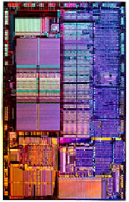
69 Intel 45nm dual-core processor die

70 Processors on an Intel 45nm Hafnium-based High-k Metal Gate ''Penryn'' Wafer photographed with an original Intel Pentium processor die. Using an entirely new transistor formula, the new processors incorporate 410 million transistors for each dual core chip, and 820 million for each quad core chip. The original Intel Pentium Processor only has 3.1 million transistors.
71
72 Introduction to IH2655 Brief historic overview Moore s Law and the ITRS Roadmap From Geometrical to Material-based scaling CMOS Process Flow
73 CMOS structures
 Silicon Nitride LPCVD deposition ( 80 nm) Photoresist spinning and")
74 CMOS Process Flow Substrate selection: moderately high resistivity, (100) orientation, P type. Wafer cleaning Thermal oxidation ( 40 nm) Silicon Nitride LPCVD deposition ( 80 nm) Photoresist spinning and baking ( μm)
75 CMOS Process Flow Mask #1 patterns the active areas Silicon Nitride is dry etched Photoresist is stripped
76 CMOS Process Flow Field oxide is grown using a LOCOS/ROX process Typically C in H 2 O grows 0.5 μm
77 CMOS Process Flow Mask #2 blocks a B + implant to form the wells for the NMOS devices Typically cm KeV
78 CMOS Process Flow Mask #3 blocks a P + implant to form the wells for the PMOS devices Typically cm KeV
79 CMOS Process Flow Annealing A high temperature drive-in produces the final well depths and repairs implant damage Typically C C
80 CMOS Process Flow Mask #4 is used to mask the PMOS devices An Implant is done on the NMOS devices Typically a 1-5 x cm -2 B KeV
81 CMOS Process Flow Mask #4 is used to mask the PMOS devices A V TH adjust implant is done on the NMOS devices Typically a 1-5 x cm -2 B KeV
82 CMOS Process Flow Mask #5 is used to mask the NMOS devices A V TH adjust implant is done on the PMOS devices, Typically 1-5 x cm -2 As KeV.
83 CMOS Process Flow The thin oxide over the active regions is stripped A high quality gate oxide grown Typically 3-5 nm, which could be grown in C in O 2 Note: Today this could be entirely different for high end technology (high-k)
84 CMOS Process Flow Polysilicon is deposited by LPCVD ( 0.5 μm) An unmasked P + or As + implant dopes the poly (typically 5 x cm -2 ) Note: Today this could be a metal gate
85 CMOS Process Flow Mask #6 is used to protect the MOS gates The poly is plasma etched using an anisotropic etch
86 CMOS Process Flow Mask #7 protects the PMOS devices A P + implant forms the LDD regions in the NMOS devices Typically 5 x cm 50 KeV
87 CMOS Process Flow Mask #8 protects the NMOS devices A B + implant forms the LDD regions in the PMOS devices Typically 5 x cm 50 KeV

88 CMOS Process Flow Conformal layer of SiO 2 is deposited (typically 0.5 μm)
89 CMOS Process Flow Anisotropic etching leaves sidewall spacers along the edges of the poly gates
90 CMOS Process Flow Mask #9 protects the PMOS devices An As + implant forms the NMOS source and drain regions Typically 2-4 x cm 75 KeV

91 CMOS Process Flow Intermetal dielectric and second level metal are deposited and defined in the same way as level #1. Mask #14 is used to define contact vias and Mask #15 is used to define metal 2 A final passivation layer of Si 3 N 4 is deposited by PECVD and patterned with Mask #16 This completes the CMOS structure

92 CMOS Process Flow Final result of the process flow: One NMOS and one PMOS device, BUT... They were made in parrallel and we can make 1 Billion other at the same time
Integrated Circuit Technology (Course Code: EE662) Lecture 1: Introduction
 Lecture 1: Introduction") Indian Institute of Technology Jodhpur, Year 2015 2016 Integrated Circuit Technology (Course Code: EE662) Lecture 1: Introduction Course Instructor: Shree Prakash Tiwari, Ph.D. Email: sptiwari@iitj.ac.in
Indian Institute of Technology Jodhpur, Year 2015 2016 Integrated Circuit Technology (Course Code: EE662) Lecture 1: Introduction Course Instructor: Shree Prakash Tiwari, Ph.D. Email: sptiwari@iitj.ac.in
EMT 251 Introduction to IC Design
 EMT 251 Introduction to IC Design (Pengantar Rekabentuk Litar Terkamir) Semester II 2011/2012 Introduction to IC design and Transistor Fundamental Some Keywords! Very-large-scale-integration (VLSI) is
Transistor was first invented by William.B.Shockley, Walter Brattain and John Bardeen of Bell Labratories. In 1961, first IC was introduced.
 Unit 1 Basic MOS Technology Transistor was first invented by William.B.Shockley, Walter Brattain and John Bardeen of Bell Labratories. In 1961, first IC was introduced. Levels of Integration:- i) SSI:-
VLSI Design. Introduction
 VLSI Design Introduction Outline Introduction Silicon, pn-junctions and transistors A Brief History Operation of MOS Transistors CMOS circuits Fabrication steps for CMOS circuits Introduction Integrated
ECE 5745 Complex Digital ASIC Design Topic 2: CMOS Devices
 ECE 5745 Complex Digital ASIC Design Topic 2: CMOS Devices Christopher Batten School of Electrical and Computer Engineering Cornell University http://www.csl.cornell.edu/courses/ece5950 Simple Transistor
Topic 3. CMOS Fabrication Process
 Topic 3 CMOS Fabrication Process Peter Cheung Department of Electrical & Electronic Engineering Imperial College London URL: www.ee.ic.ac.uk/pcheung/ E-mail: p.cheung@ic.ac.uk Lecture 3-1 Layout of a Inverter
Introduction to VLSI ASIC Design and Technology
 Introduction to VLSI ASIC Design and Technology Paulo Moreira CERN - Geneva, Switzerland Paulo Moreira Introduction 1 Outline Introduction Is there a limit? Transistors CMOS building blocks Parasitics
Progress due to: Feature size reduction - 0.7X/3 years (Moore s Law). Increasing chip size - 16% per year. Creativity in implementing functions.
. Increasing chip size - 16% per year. Creativity in implementing functions.") Introduction - Chapter 1 Evolution of IC Fabrication 1960 and 1990 integrated t circuits. it Progress due to: Feature size reduction - 0.7X/3 years (Moore s Law). Increasing chip size - 16% per year. Creativity
Introduction - Chapter 1 Evolution of IC Fabrication 1960 and 1990 integrated t circuits. it Progress due to: Feature size reduction - 0.7X/3 years (Moore s Law). Increasing chip size - 16% per year. Creativity
EE4800 CMOS Digital IC Design & Analysis. Lecture 1 Introduction Zhuo Feng
 EE4800 CMOS Digital IC Design & Analysis Lecture 1 Introduction Zhuo Feng 1.1 Prof. Zhuo Feng Office: EERC 730 Phone: 487-3116 Email: zhuofeng@mtu.edu Class Website http://www.ece.mtu.edu/~zhuofeng/ee4800fall2010.html
VLSI Design. Introduction
 Tassadaq Hussain VLSI Design Introduction Outcome of this course Problem Aims Objectives Outcomes Data Collection Theoretical Model Mathematical Model Validate Development Analysis and Observation Pseudo
MICROPROCESSOR TECHNOLOGY
 MICROPROCESSOR TECHNOLOGY Assis. Prof. Hossam El-Din Moustafa Lecture 3 Ch.1 The Evolution of The Microprocessor 17-Feb-15 1 Chapter Objectives Introduce the microprocessor evolution from transistors to
Layout of a Inverter. Topic 3. CMOS Fabrication Process. The CMOS Process - photolithography (2) The CMOS Process - photolithography (1) v o.
 The CMOS Process - photolithography (1) v o.") Layout of a Inverter Topic 3 CMOS Fabrication Process V DD Q p Peter Cheung Department of Electrical & Electronic Engineering Imperial College London v i v o Q n URL: www.ee.ic.ac.uk/pcheung/ E-mail: p.cheung@ic.ac.uk
Layout of a Inverter Topic 3 CMOS Fabrication Process V DD Q p Peter Cheung Department of Electrical & Electronic Engineering Imperial College London v i v o Q n URL: www.ee.ic.ac.uk/pcheung/ E-mail: p.cheung@ic.ac.uk
Introduction to Electronic Devices
 (Course Number 300331) Fall 2006 Instructor: Dr. Dietmar Knipp Assistant Professor of Electrical Engineering Information: http://www.faculty.iubremen.de/dknipp/ Source: Apple Ref.: Apple Ref.: IBM Critical
CMOS Digital Integrated Circuits Lec 2 Fabrication of MOSFETs
 CMOS Digital Integrated Circuits Lec 2 Fabrication of MOSFETs 1 CMOS Digital Integrated Circuits 3 rd Edition Categories of Materials Materials can be categorized into three main groups regarding their
Chapter 1, Introduction
 Introduction to Semiconductor Manufacturing Technology Chapter 1, Introduction hxiao89@hotmail.com 1 Objective After taking this course, you will able to Use common semiconductor terminology Describe a
420 Intro to VLSI Design
 Dept of Electrical and Computer Engineering 420 Intro to VLSI Design Lecture 0: Course Introduction and Overview Valencia M. Joyner Spring 2005 Getting Started Syllabus About the Instructor Labs, Problem
Lecture 0: Introduction
 Lecture 0: Introduction Introduction Integrated circuits: many transistors on one chip. Very Large Scale Integration (VLSI): bucketloads! Complementary Metal Oxide Semiconductor Fast, cheap, low power
Lecture 020 ECE4430 Review II (1/5/04) Page 020-1
 Page 020-1") Lecture 020 ECE4430 Review II (1/5/04) Page 020-1 LECTURE 020 ECE 4430 REVIEW II (READING: GHLM - Chap. 2) Objective The objective of this presentation is: 1.) Identify the prerequisite material as taught
Lecture 020 ECE4430 Review II (1/5/04) Page 020-1 LECTURE 020 ECE 4430 REVIEW II (READING: GHLM - Chap. 2) Objective The objective of this presentation is: 1.) Identify the prerequisite material as taught
+1 (479)
") Introduction to VLSI Design http://csce.uark.edu +1 (479) 575-6043 yrpeng@uark.edu Invention of the Transistor Vacuum tubes ruled in first half of 20th century Large, expensive, power-hungry, unreliable
Introduction to VLSI Design http://csce.uark.edu +1 (479) 575-6043 yrpeng@uark.edu Invention of the Transistor Vacuum tubes ruled in first half of 20th century Large, expensive, power-hungry, unreliable
VLSI Technology Dr. Nandita Dasgupta Department of Electrical Engineering Indian Institute of Technology, Madras
 VLSI Technology Dr. Nandita Dasgupta Department of Electrical Engineering Indian Institute of Technology, Madras Lecture - 40 BICMOS technology So, today we are going to have the last class on this VLSI
Silicon VLSI Technology. Fundamentals, Practice and Modeling. Class Notes For Instructors. J. D. Plummer, M. D. Deal and P. B.
 Silicon VLSI Technology Fundamentals, ractice, and Modeling Class otes For Instructors J. D. lummer, M. D. Deal and. B. Griffin These notes are intended to be used for lectures based on the above text.
Lecture 1 Introduction to Solid State Electronics
 EE 471: Transport Phenomena in Solid State Devices Spring 2018 Lecture 1 Introduction to Solid State Electronics Bryan Ackland Department of Electrical and Computer Engineering Stevens Institute of Technology
EE 5611 Introduction to Microelectronic Technologies Fall Thursday, September 04, 2014 Lecture 02
 EE 5611 Introduction to Microelectronic Technologies Fall 2014 Thursday, September 04, 2014 Lecture 02 1 Lecture Outline Review on semiconductor materials Review on microelectronic devices Example of microelectronic
Chapter 3: Basics Semiconductor Devices and Processing 2006/9/27 1. Topics
 Chapter 3: Basics Semiconductor Devices and Processing 2006/9/27 1 Topics What is semiconductor Basic semiconductor devices Basics of IC processing CMOS technologies 2006/9/27 2 1 What is Semiconductor
Lecture 27 ANNOUNCEMENTS. Regular office hours will end on Monday 12/10 Special office hours will be posted on the EE105 website
 Lecture 27 ANNOUNCEMENTS Regular office hours will end on Monday 12/10 Special office hours will be posted on the EE105 website Final Exam Review Session: Friday 12/14, 3PM, HP Auditorium Video will be
Design cycle for MEMS
 Design cycle for MEMS Design cycle for ICs IC Process Selection nmos CMOS BiCMOS ECL for logic for I/O and driver circuit for critical high speed parts of the system The Real Estate of a Wafer MOS Transistor
EE 410: Integrated Circuit Fabrication Laboratory
 EE 410: Integrated Circuit Fabrication Laboratory 1 EE 410: Integrated Circuit Fabrication Laboratory Web Site: Instructor: http://www.stanford.edu/class/ee410 https://ccnet.stanford.edu/ee410/ (on CCNET)
Lecture 33 - The Short Metal-Oxide-Semiconductor Field-Effect Transistor (cont.) April 30, 2007
 April 30, 2007") 6.720J/3.43J - Integrated Microelectronic Devices - Spring 2007 Lecture 33-1 Lecture 33 - The Short Metal-Oxide-Semiconductor Field-Effect Transistor (cont.) April 30, 2007 Contents: 1. MOSFET scaling
6.720J/3.43J - Integrated Microelectronic Devices - Spring 2007 Lecture 33-1 Lecture 33 - The Short Metal-Oxide-Semiconductor Field-Effect Transistor (cont.) April 30, 2007 Contents: 1. MOSFET scaling
ECE520 VLSI Design. Lecture 2: Basic MOS Physics. Payman Zarkesh-Ha
 ECE520 VLSI Design Lecture 2: Basic MOS Physics Payman Zarkesh-Ha Office: ECE Bldg. 230B Office hours: Wednesday 2:00-3:00PM or by appointment E-mail: pzarkesh@unm.edu Slide: 1 Review of Last Lecture Semiconductor
2.8 - CMOS TECHNOLOGY
 CMOS Technology (6/7/00) Page 1 2.8 - CMOS TECHNOLOGY INTRODUCTION Objective The objective of this presentation is: 1.) Illustrate the fabrication sequence for a typical MOS transistor 2.) Show the physical
Selected Topics in Nanoelectronics. Danny Porath 2002
 Selected Topics in Nanoelectronics Danny Porath 2002 Links to NST http://www.foresight.org/ http://itri.loyola.edu/nanobase/ http://www.zyvex.com/nano/ http://www.nano.gov/ http://www.aeiveos.com/nanotech/
EECS 151/251A Spring 2019 Digital Design and Integrated Circuits. Instructors: Wawrzynek. Lecture 8 EE141
 EECS 151/251A Spring 2019 Digital Design and Integrated Circuits Instructors: Wawrzynek Lecture 8 EE141 From the Bottom Up IC processing CMOS Circuits (next lecture) EE141 2 Overview of Physical Implementations
Chapter 3 Basics Semiconductor Devices and Processing
 Chapter 3 Basics Semiconductor Devices and Processing 1 Objectives Identify at least two semiconductor materials from the periodic table of elements List n-type and p-type dopants Describe a diode and
Advanced Digital Integrated Circuits. Lecture 2: Scaling Trends. Announcements. No office hour next Monday. Extra office hour Tuesday 2-3pm
 EE241 - Spring 20 Advanced Digital Integrated Circuits Lecture 2: Scaling Trends and Features of Modern Technologies Announcements No office hour next Monday Extra office hour Tuesday 2-3pm 2 1 Outline
EECS130 Integrated Circuit Devices
 EECS130 Integrated Circuit Devices Professor Ali Javey 11/6/2007 MOSFETs Lecture 6 BJTs- Lecture 1 Reading Assignment: Chapter 10 More Scalable Device Structures Vertical Scaling is important. For example,
MOSFET & IC Basics - GATE Problems (Part - I)
") MOSFET & IC Basics - GATE Problems (Part - I) 1. Channel current is reduced on application of a more positive voltage to the GATE of the depletion mode n channel MOSFET. (True/False) [GATE 1994: 1 Mark]
MOSFET & IC Basics - GATE Problems (Part - I) 1. Channel current is reduced on application of a more positive voltage to the GATE of the depletion mode n channel MOSFET. (True/False) [GATE 1994: 1 Mark]
EE669: VLSI TECHNOLOGY
 EE669: VLSI TECHNOLOGY Autumn Semester Graduate Course 2014-2015 Session by Arun N. Chandorkar Emeritus Fellow Professor Department of Electrical Engineering Indian Institute of Technology, Bombay Powai,
Semiconductor Devices
 Semiconductor Devices - 2014 Lecture Course Part of SS Module PY4P03 Dr. P. Stamenov School of Physics and CRANN, Trinity College, Dublin 2, Ireland Hilary Term, TCD 3 th of Feb 14 MOSFET Unmodified Channel
Lecture 8. MOS Transistors; Cheap Computers; Everycircuit
 Lecture 8 MOS Transistors; Cheap Computers; Everycircuit Copyright 2017 by Mark Horowitz 1 Reading The rest of Chapter 4 in the reader For more details look at A&L 5.1 Digital Signals (goes in much more
CMOS Technology. 1. Why CMOS 2. Qualitative MOSFET model 3. Building a MOSFET 4. CMOS logic gates. Handouts: Lecture Slides. metal ndiff.
 CMOS Technology 1. Why CMOS 2. Qualitative MOSFET model 3. Building a MOSFET 4. CMOS logic gates poly pdiff metal ndiff Handouts: Lecture Slides L03 - CMOS Technology 1 Building Bits from Atoms V in V
Sub-micron technology IC fabrication process trends SOI technology. Development of CMOS technology. Technology problems due to scaling
 Goodbye Microelectronics Welcome Nanoelectronics Sub-micron technology IC fabrication process trends SOI technology SiGe Tranzistor in 50nm process Virus The thickness of gate oxide= 1.2 nm!!! Today we
FABRICATION OF CMOS INTEGRATED CIRCUITS. Dr. Mohammed M. Farag
 FABRICATION OF CMOS INTEGRATED CIRCUITS Dr. Mohammed M. Farag Outline Overview of CMOS Fabrication Processes The CMOS Fabrication Process Flow Design Rules Reference: Uyemura, John P. "Introduction to
problem grade total
 Fall 2005 6.012 Microelectronic Devices and Circuits Prof. J. A. del Alamo Name: Recitation: November 16, 2005 Quiz #2 problem grade 1 2 3 4 total General guidelines (please read carefully before starting):
Newer process technology (since 1999) includes :
 includes :") Newer process technology (since 1999) includes : copper metalization hi-k dielectrics for gate insulators si on insulator strained silicon lo-k dielectrics for interconnects Immersion lithography for masks
Newer process technology (since 1999) includes : copper metalization hi-k dielectrics for gate insulators si on insulator strained silicon lo-k dielectrics for interconnects Immersion lithography for masks
ISSCC 2003 / SESSION 1 / PLENARY / 1.1
 ISSCC 2003 / SESSION 1 / PLENARY / 1.1 1.1 No Exponential is Forever: But Forever Can Be Delayed! Gordon E. Moore Intel Corporation Over the last fifty years, the solid-state-circuits industry has grown
Characterization of SOI MOSFETs by means of charge-pumping
 Paper Characterization of SOI MOSFETs by means of charge-pumping Grzegorz Głuszko, Sławomir Szostak, Heinrich Gottlob, Max Lemme, and Lidia Łukasiak Abstract This paper presents the results of charge-pumping
ECE-606: Spring Course Introduction
 ECE-606: Spring 2013 Course Introduction Professor Mark Lundstrom Electrical and Computer Engineering Purdue University, West Lafayette, IN USA lundstro@purdue.edu 1/8/13 1 course objectives To introduce
State-of-the-art device fabrication techniques
 State-of-the-art device fabrication techniques! Standard Photo-lithography and e-beam lithography! Advanced lithography techniques used in semiconductor industry Deposition: Thermal evaporation, e-gun
ADVANCED MATERIALS AND PROCESSES FOR NANOMETER-SCALE FINFETS
 ADVANCED MATERIALS AND PROCESSES FOR NANOMETER-SCALE FINFETS Tsu-Jae King, Yang-Kyu Choi, Pushkar Ranade^ and Leland Chang Electrical Engineering and Computer Sciences Dept., ^Materials Science and Engineering
Assoc. Prof. Dr. MONTREE SIRIPRUCHYANUN
 1 Assoc. Prof. Dr. MONTREE SIRIPRUCHYANUN Dept. of Teacher Training in Electrical Engineering 1 King Mongkut s Institute of Technology North Bangkok 1929 Bulky, expensive and required high supply voltages.
New Process Technologies Will silicon CMOS carry us to the end of the Roadmap?
 HPEC Workshop 2006 New Process Technologies Will silicon CMOS carry us to the end of the Roadmap? Craig L. Keast, Chenson Chen, Mike Fritze, Jakub Kedzierski, Dave Shaver HPEC 2006-1 Outline A brief history
ITRS MOSFET Scaling Trends, Challenges, and Key Technology Innovations
 Workshop on Frontiers of Extreme Computing Santa Cruz, CA October 24, 2005 ITRS MOSFET Scaling Trends, Challenges, and Key Technology Innovations Peter M. Zeitzoff Outline Introduction MOSFET scaling and
Session 3: Solid State Devices. Silicon on Insulator
 Session 3: Solid State Devices Silicon on Insulator 1 Outline A B C D E F G H I J 2 Outline Ref: Taurand Ning 3 SOI Technology SOl materials: SIMOX, BESOl, and Smart Cut SIMOX : Synthesis by IMplanted
ECSE-6300 IC Fabrication Laboratory Lecture 9 MOSFETs. Lecture Outline
 ECSE-6300 IC Fabrication Laboratory Lecture 9 MOSFETs Prof. Rensselaer Polytechnic Institute Troy, NY 12180 Office: CII-6229 Tel.: (518) 276-2909 e-mails: luj@rpi.edu http://www.ecse.rpi.edu/courses/s18/ecse
Photolithography I ( Part 1 )
") 1 Photolithography I ( Part 1 ) Chapter 13 : Semiconductor Manufacturing Technology by M. Quirk & J. Serda Bjørn-Ove Fimland, Department of Electronics and Telecommunication, Norwegian University of Science
1 Photolithography I ( Part 1 ) Chapter 13 : Semiconductor Manufacturing Technology by M. Quirk & J. Serda Bjørn-Ove Fimland, Department of Electronics and Telecommunication, Norwegian University of Science
Introduction to Materials Engineering: Materials Driving the Electronics Revolution Robert Hull, MSE
 Introduction to Materials Engineering: Materials Driving the Electronics Revolution Robert Hull, MSE Outline Microelectronics Miniaturization Historical Development: Electronics before Semiconductors The
Semiconductor Physics and Devices
 Metal-Semiconductor and Semiconductor Heterojunctions The Metal-Oxide-Semiconductor Field-Effect Transistor (MOSFET) is one of two major types of transistors. The MOSFET is used in digital circuit, because
FinFET vs. FD-SOI Key Advantages & Disadvantages
 FinFET vs. FD-SOI Key Advantages & Disadvantages Amiad Conley Technical Marketing Manager Process Diagnostics & Control, Applied Materials ChipEx-2014, Apr 2014 1 Moore s Law The number of transistors
Lecture #29. Moore s Law
 Lecture #29 ANNOUNCEMENTS HW#15 will be for extra credit Quiz #6 (Thursday 5/8) will include MOSFET C-V No late Projects will be accepted after Thursday 5/8 The last Coffee Hour will be held this Thursday
Challenges and Innovations in Nano CMOS Transistor Scaling
 Challenges and Innovations in Nano CMOS Transistor Scaling Tahir Ghani Intel Fellow Logic Technology Development October, 2009 Nikkei Presentation 1 Outline Traditional Scaling Traditional Scaling Limiters,
EECS130 Integrated Circuit Devices
 EECS130 Integrated Circuit Devices Professor Ali Javey 11/01/2007 MOSFETs Lecture 5 Announcements HW7 set is due now HW8 is assigned, but will not be collected/graded. MOSFET Technology Scaling Technology
6.012 Microelectronic Devices and Circuits
 MIT, Spring 2009 6.012 Microelectronic Devices and Circuits Charles G. Sodini Jing Kong Shaya Famini, Stephanie Hsu, Ming Tang Lecture 1 6.012 Overview Contents: Overview of 6.012 Reading Assignment: Howe
Alternatives to standard MOSFETs. What problems are we really trying to solve?
 Alternatives to standard MOSFETs A number of alternative FET schemes have been proposed, with an eye toward scaling up to the 10 nm node. Modifications to the standard MOSFET include: Silicon-in-insulator
ECEN474/704: (Analog) VLSI Circuit Design Fall 2016
 VLSI Circuit Design Fall 2016") ECEN474/704: (Analog) VLSI Circuit Design Fall 2016 Lecture 1: Introduction Sam Palermo Analog & Mixed-Signal Center Texas A&M University Announcements Turn in your 0.18um NDA form by Thursday Sep 1 No
ECEN474/704: (Analog) VLSI Circuit Design Fall 2016 Lecture 1: Introduction Sam Palermo Analog & Mixed-Signal Center Texas A&M University Announcements Turn in your 0.18um NDA form by Thursday Sep 1 No
Design Simulation and Analysis of NMOS Characteristics for Varying Oxide Thickness
 MIT International Journal of Electronics and Communication Engineering, Vol. 4, No. 2, August 2014, pp. 81 85 81 Design Simulation and Analysis of NMOS Characteristics for Varying Oxide Thickness Alpana
Chapter 15 Summary and Future Trends
 Chapter 15 Summary and Future Trends Hong Xiao, Ph. D. hxiao89@hotmail.com www2.austin.cc.tx.us/hongxiao/book.htm Hong Xiao, Ph. D. www2.austin.cc.tx.us/hongxiao/book.htm 1 The 1960s First IC product Bipolar
EE241 - Spring 2013 Advanced Digital Integrated Circuits. Announcements. Sign up for Piazza if you haven t already
 EE241 - Spring 2013 Advanced Digital Integrated Circuits Lecture 2: Scaling Trends and Features of Modern Technologies Announcements Sign up for Piazza if you haven t already 2 1 Assigned Reading R.H.
Integrated diodes. The forward voltage drop only slightly depends on the forward current. ELEKTRONIKOS ĮTAISAI
 1 Integrated diodes pn junctions of transistor structures can be used as integrated diodes. The choice of the junction is limited by the considerations of switching speed and breakdown voltage. The forward
Future MOSFET Devices using high-k (TiO 2 ) dielectric
 dielectric") Future MOSFET Devices using high-k (TiO 2 ) dielectric Prerna Guru Jambheshwar University, G.J.U.S. & T., Hisar, Haryana, India, prernaa.29@gmail.com Abstract: In this paper, an 80nm NMOS with high-k (TiO
Future MOSFET Devices using high-k (TiO 2 ) dielectric Prerna Guru Jambheshwar University, G.J.U.S. & T., Hisar, Haryana, India, prernaa.29@gmail.com Abstract: In this paper, an 80nm NMOS with high-k (TiO
Performance investigations of novel dual-material gate (DMG) MOSFET with dielectric pockets (DP)
 MOSFET with dielectric pockets (DP)") Science in China Series E: Technological Sciences 2009 SCIENCE IN CHINA PRESS www.scichina.com tech.scichina.com Performance investigations of novel dual-material gate (DMG) MOSFET with dielectric pockets
Science in China Series E: Technological Sciences 2009 SCIENCE IN CHINA PRESS www.scichina.com tech.scichina.com Performance investigations of novel dual-material gate (DMG) MOSFET with dielectric pockets
Intel s High-k/Metal Gate Announcement. November 4th, 2003
 Intel s High-k/Metal Gate Announcement November 4th, 2003 1 What are we announcing? Intel has made significant progress in future transistor materials Two key parts of this new transistor are: The gate
PROCESS AND DEVICE SIMULATION OF 80NM CMOS INVERTER USING SENTAURUS SYNOPSYS TCAD
 052 PROCESS AND DEVICE SIMULATION OF 80NM CMOS INVERTER USING SENTAURUS SYNOPSYS TCAD Muhammad Suhaimi Sulong, Asyiatul Asyikin Jamry, Siti Maryaton Shuadah Shuib, Rahmat Sanudin, Marlia Morsin, Mohd Zainizan
EE 330 Lecture 7. Design Rules. IC Fabrication Technology Part 1
 EE 330 Lecture 7 Design Rules IC Fabrication Technology Part 1 Review from Last Time Technology Files Provide Information About Process Process Flow (Fabrication Technology) Model Parameters Design Rules
SPECIAL REPORT SOI Wafer Technology for CMOS ICs
 SPECIAL REPORT SOI Wafer Technology for CMOS ICs Robert Simonton President, Simonton Associates Introduction: SOI (Silicon On Insulator) wafers have been used commercially as starting substrates for several
Semiconductor Physics and Devices
 Nonideal Effect The experimental characteristics of MOSFETs deviate to some degree from the ideal relations that have been theoretically derived. Semiconductor Physics and Devices Chapter 11. MOSFET: Additional
EE C245 / ME C218 INTRODUCTION TO MEMS DESIGN FALL 2011 PROBLEM SET #2. Due (at 7 p.m.): Tuesday, Sept. 27, 2011, in the EE C245 HW box in 240 Cory.
: Tuesday, Sept. 27, 2011, in the EE C245 HW box in 240 Cory.") Issued: Tuesday, Sept. 13, 2011 PROBLEM SET #2 Due (at 7 p.m.): Tuesday, Sept. 27, 2011, in the EE C245 HW box in 240 Cory. 1. Below in Figure 1.1 is a description of a DRIE silicon etch using the Marvell
Issued: Tuesday, Sept. 13, 2011 PROBLEM SET #2 Due (at 7 p.m.): Tuesday, Sept. 27, 2011, in the EE C245 HW box in 240 Cory. 1. Below in Figure 1.1 is a description of a DRIE silicon etch using the Marvell
ATV 2011: Computer Engineering
 ATV 2011: Technology Trends in Computer Engineering Professor Per Larsson-Edefors ATV 2011, L1, Per Larsson-Edefors Page 1 Solid-State Devices www.cse.chalmers.se/~perla/ugrad/ SemTech/Lectures_2000.pdf
Notes. (Subject Code: 7EC5)
") COMPUCOM INSTITUTE OF TECHNOLOGY & MANAGEMENT, JAIPUR (DEPARTMENT OF ELECTRONICS & COMMUNICATION) Notes VLSI DESIGN NOTES (Subject Code: 7EC5) Prepared By: MANVENDRA SINGH Class: B. Tech. IV Year, VII
COMPUCOM INSTITUTE OF TECHNOLOGY & MANAGEMENT, JAIPUR (DEPARTMENT OF ELECTRONICS & COMMUNICATION) Notes VLSI DESIGN NOTES (Subject Code: 7EC5) Prepared By: MANVENDRA SINGH Class: B. Tech. IV Year, VII
Lecture: Integration of silicon photonics with electronics. Prepared by Jean-Marc FEDELI CEA-LETI
 Lecture: Integration of silicon photonics with electronics Prepared by Jean-Marc FEDELI CEA-LETI Context The goal is to give optical functionalities to electronics integrated circuit (EIC) The objectives
Low-Frequency Noise in High-k LaLuO 3 /TiN MOSFETs
 Low-Frequency Noise in High-k LaLuO 3 /TiN MOSFETs Maryam Olyaei, B. Gunnar Malm, Per-Erik Hellström, and Mikael Östling KTH Royal Institute of Technology, Integrated Devices and Circuits, School of Information
6.012 Microelectronic Devices and Circuits
 MIT, Spring 2003 6.012 Microelectronic Devices and Circuits Jesús del Alamo Dimitri Antoniadis, Judy Hoyt, Charles Sodini Pablo Acosta, Susan Luschas, Jorg Scholvin, Niamh Waldron Lecture 1 6.012 overview
Semiconductor TCAD Tools
 Device Design Consideration for Nanoscale MOSFET Using Semiconductor TCAD Tools Teoh Chin Hong and Razali Ismail Department of Microelectronics and Computer Engineering, Universiti Teknologi Malaysia,
Practical Information
 EE241 - Spring 2013 Advanced Digital Integrated Circuits MW 2-3:30pm 540A/B Cory Practical Information Instructor: Borivoje Nikolić 509 Cory Hall, 3-9297, bora@eecs Office hours: M 11-12, W 3:30pm-4:30pm
Basic Fabrication Steps
 Basic Fabrication Steps and Layout Somayyeh Koohi Department of Computer Engineering Adapted with modifications from lecture notes prepared by author Outline Fabrication steps Transistor structures Transistor
Student Lecture by: Giangiacomo Groppi Joel Cassell Pierre Berthelot September 28 th 2004
 Student Lecture by: Giangiacomo Groppi Joel Cassell Pierre Berthelot September 28 th 2004 Lecture outline Historical introduction Semiconductor devices overview Bipolar Junction Transistor (BJT) Field
Intel Demonstrates High-k + Metal Gate Transistor Breakthrough on 45 nm Microprocessors
 Intel Demonstrates High-k + Metal Gate Transistor Breakthrough on 45 nm Microprocessors Mark Bohr Intel Senior Fellow Logic Technology Development Kaizad Mistry 45 nm Program Manager Logic Technology Development
INTRODUCTION TO MOS TECHNOLOGY
 INTRODUCTION TO MOS TECHNOLOGY 1. The MOS transistor The most basic element in the design of a large scale integrated circuit is the transistor. For the processes we will discuss, the type of transistor
ECE 2300 Digital Logic & Computer Organization
 ECE 2300 Digital Logic & Computer Organization Spring 2018 CMOS Logic Lecture 4: 1 NAND Logic Gate X Y (X Y) = NAND Using De Morgan s Law: (X Y) = X +Y X X X +Y = Y Y Also a NAND We can build circuits
Lecture Integrated circuits era
 Lecture 1 1.1 Integrated circuits era Transistor was first invented by William.B.Shockley, Walter Brattain and John Bardeen of Bell laboratories. In 1961, first IC was introduced. Levels of Integration:-
Final Exam Topics. IC Technology Advancement. Microelectronics Technology in the 21 st Century. Intel s 90 nm CMOS Technology. 14 nm CMOS Transistors
 ANNOUNCEMENTS Final Exam: When: Wednesday 12/10 12:30-3:30PM Where: 10 Evans (last names beginning A-R) 60 Evans (last names beginning S-Z) Comprehensive coverage of course material Closed book; 3 sheets
ECSE-6300 IC Fabrication Laboratory Lecture 7 MOSFETs. Lecture Outline
 ECSE-6300 IC Fabrication Laboratory Lecture 7 MOSFETs Prof. Rensselaer Polytechnic Institute Troy, NY 12180 Office: CII-6229 Tel.: (518) 276-2909 e-mails: luj@rpi.edu http://www.ecse.rpi.edu/courses/s16/ecse
Drain. Drain. [Intel: bulk-si MOSFETs]
![Drain. Drain. [Intel: bulk-si MOSFETs]](/thumbs/89/97695223.jpg "Drain. Drain. [Intel: bulk-si MOSFETs]") 1 Introduction For more than 40 years, the evolution and growth of very-large-scale integration (VLSI) silicon-based integrated circuits (ICs) have followed from the continual shrinking, or scaling, of
1 Introduction For more than 40 years, the evolution and growth of very-large-scale integration (VLSI) silicon-based integrated circuits (ICs) have followed from the continual shrinking, or scaling, of
EE301 Electronics I , Fall
 EE301 Electronics I 2018-2019, Fall 1. Introduction to Microelectronics (1 Week/3 Hrs.) Introduction, Historical Background, Basic Consepts 2. Rewiev of Semiconductors (1 Week/3 Hrs.) Semiconductor materials
UNIT III VLSI CIRCUIT DESIGN PROCESSES. In this chapter we will be studying how to get the schematic into stick diagrams or layouts.
 UNIT III VLSI CIRCUIT DESIGN PROCESSES In this chapter we will be studying how to get the schematic into stick diagrams or layouts. MOS circuits are formed on four basic layers: N-diffusion P-diffusion
The Design and Realization of Basic nmos Digital Devices
 Proceedings of The National Conference On Undergraduate Research (NCUR) 2004 Indiana University Purdue University Indianapolis, Indiana April 15-17, 2004 The Design and Realization of Basic nmos Digital
In this lecture we will begin a new topic namely the Metal-Oxide-Semiconductor Field Effect Transistor.
 Solid State Devices Dr. S. Karmalkar Department of Electronics and Communication Engineering Indian Institute of Technology, Madras Lecture - 38 MOS Field Effect Transistor In this lecture we will begin
SAMPLE SLIDES & COURSE OUTLINE. Core Competency In Semiconductor Technology: 2. FABRICATION. Dr. Theodore (Ted) Dellin
 Dellin") & Digging Deeper Devices, Fabrication & Reliability For More Info:.com or email Dellin@ieee.org SAMPLE SLIDES & COURSE OUTLINE In : 2. A Easy, Effective, of How Devices Are.. Recommended for everyone who
& Digging Deeper Devices, Fabrication & Reliability For More Info:.com or email Dellin@ieee.org SAMPLE SLIDES & COURSE OUTLINE In : 2. A Easy, Effective, of How Devices Are.. Recommended for everyone who
FET. Field Effect Transistors ELEKTRONIKA KONTROL. Eka Maulana, ST, MT, M.Eng. Universitas Brawijaya. p + S n n-channel. Gate. Basic structure.
 FET Field Effect Transistors ELEKTRONIKA KONTROL Basic structure Gate G Source S n n-channel Cross section p + p + p + G Depletion region Drain D Eka Maulana, ST, MT, M.Eng. Universitas Brawijaya S Channel
Practical Information
 EE241 - Spring 2010 Advanced Digital Integrated Circuits TuTh 3:30-5pm 293 Cory Practical Information Instructor: Borivoje Nikolić 550B Cory Hall, 3-9297, bora@eecs Office hours: M 10:30am-12pm Reader: