Assoc. Prof. Dr. MONTREE SIRIPRUCHYANUN
|
|
|
- May Pope
- 5 years ago
- Views:
Transcription

1 1 Assoc. Prof. Dr. MONTREE SIRIPRUCHYANUN Dept. of Teacher Training in Electrical Engineering 1 King Mongkut s Institute of Technology North Bangkok 1929 Bulky, expensive and required high supply voltages. 2


2 2 IEEE J. Solid-State Circuits, Vol. 32, 12, pp ,

3 3 5 6
, 1947 John Bardeen and Walter Brattain")
, 1958 Jack S.")

4 Audion (Triode), 1906 Lee De Forest First point contact transistor (germanium), 1947 John Bardeen and Walter Brattain Bell Laboratories First integrated circuit (germanium), 1958 Jack S. Kilby, Texas Instruments Contained five components, three types: transistors resistors and capacitors Intel Pentium II, 1997 Clock: 233MHz Number of transistors: 7.5 M Gate Length:

5 5 Number of transistors doubles every 2.3 years (acceleration over the last 4 years: 1.5 years) 42 M transistors Increase: ~20K 2.25 K transistors (From: GHz Intel Labs Sub-ps switching transistor μp clock > 20 GHz Gate length: 20nm Gate oxide: 3 atomic layers In production: 2007! 10
 Road Map, 1998 Update 1999 2002 2014 Technology (nm) 180 130 35 Minimum mask count 22/24 24 29/30 Wafer diameter (mm) 300 300 450")
6 6 Intel Labs Sub-ps switching transistor μp clock > 20 GHz Gate length: 20nm Gate oxide: 3 atomic layers In production: 2007! 0.13 μm in production 11 Semiconductor Industry Association (SIA) Road Map, 1998 Update Technology (nm) Minimum mask count 22/ /30 Wafer diameter (mm) Memory-samples (bits) 1G 4G 1T Transistors/cm 2 (μp) 6.2M 18M 390M Wiring levels (maximum) Clock, local (MHz) Chip size: DRAM (mm 2 ) Chip size: μp (mm 2 ) Power supply (V) Maximum Power (W) Number of pins (μp) IEEE Spectrum, July 1999 Special report: The 100-million transistor IC These scaling trends will allow the electronics market to growth at 15% / year 12
7 7 1% GaAs and others % 19% 22% ECL TTL and OTHER BIPOLAR ANALOG 4% 12% 20% 10% 70% 8% BIPOLAR % 41% PMOS NMOS 24% CMOS 86 % MOS 20 39% BiCMOS 10 12% 16% 4% Year Gate Length (nm) DD Trend of supply voltage and 1/f noise from 2003 ITRS Roadmap 14

8 Gate Length (nm) Peak f max Peak f T min Trend of supply voltage and 1/f noise from 2003 ITRS Roadmap 15 Si CMOS displacement of other technologies continues Boundary between GaAs & InP shifting to lower frequencies Cost is a key factor in determining boundaries ITRS 2003 Roadmap, RF and AMS Technologies for Wireless Communications 16

 reduces the threshold voltage V T low voltage applications Forward substrate")
9 9 kabuki.eecs.berkeley.edu/~jrudell/ IEEE Spectrum, March 2002 Using standard, mature CMOS processes to design RFIC building blocks With CMOS, DSP blocks can be integrated with RF frontend on the same chip good IP 17 integration Drain Current (A) G V GS 0.5V 0V -0.5V D S V DS B V BS NMOS, 10x0.2μm V DS =25mV V BS improves the MOSFET performance Forward substrate biasing (V BS >0) reduces the threshold voltage V T low voltage applications Forward substrate biasing (V BS >0) speeds - up the MOSFET RF applications Reverse substrate biasing (V BS <0) reduces the drain current I D low power applications Gate Voltage (V) 18
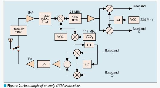
10 10 Operate transistor in weak inversion Very low V DS required to operate transistor low-voltage applications Drain current I D also very low low-power applications I D (A) Calculation Measured V DS (V) V V GS =-0.01V Proc. ISCAS, pp. I697-I700 and I701-I704, Bangkok, Thailand (May 25-28, 2003) 19 Duplexer LNA PA Band-pass filter Band-pass filter LO ADC Channel select DAC Low frequency signal processing Small Signal RF Power Management Analog Baseband Power RF Digital Baseband (DSP + MCU) bwrc.eecs.berkeley.edu Proc. IEEE EDSSC, Hong Kong, December


11 11 m V DD Buffer IF+ (to buffer) LO+ R L R L LO- IF- (to buffer) LO+ RF- RF+ I BIAS Supply voltage/power 1.2V/3.95mW SSB Noise Figure/IIP3 17dB/8dBm RF Input/Conversion Gain 1.9GHz/-2dB FoM/Technology 199dB/0.18μm Proc. IEEE EDSSC, Hong Kong, December V DD IF+ R L R L Buffer RF+ RF+ LO+ IF- RF- LO- V BIAS Supply voltage/power 0.8V/0.4mW RF Input/Conversion Gain 1.9GHz/3dB Proc. IEEE EDSSC, Hong Kong, December 2003 SSB Noise Figure/IIP3 FoM/Technology 10dB/-11dBm 202dB/0.18μm 22


12 12 V DD R L R L RF+ IF+ LO+ RF- IF- LO+ Buffer LO- V bias Supply voltage/power RF Input/Conv. Gain Noise Figure/IIP3 FoM/Technology 1V/1mW 2.4GHz/-4dB 10dB/-2dB 202dB/0.18μm Proc. IEEE EDSSC, Hong Kong, December Reduce number of off-chip passives Increase amount of integration Reduce number of off-chip passives Small product: Cell phone Cost effective 24


13 13 Inductor Quality factor PN Diode and MOS Varactor Tuning range Quality factor over tuning range N+ N+ N+ N Well P- Substrate Vias May become a concern as frequencies of RFIC reach the 10s of GHz range IMEC 2003, Microsystems 25 IEEE Spectrum, July


14 14 RF Design, Nov Issues Substrate noise isolation between noisy digital and low noise analog circuits Cross-talk between sensitive analog circuits Possible Solutions Careful attention to layout Multiple voltage sources Guard rings around noisy digital circuitry Double well and triple well (deep Nwell isolation) 28
15 15 Noise low frequency and SNR Matching of input stages fluctuation/dispersion effects Technology - t ox, N sub, x j V T, g m, g DS, f T, f MAX Design - L G, W G R G, g m, g DS, f T, f MAX Low-voltage design Voltage distribution across elements between V DD and V SS Modeling in subthreshold Novel circuits required Modeling of passives and improved passives Isolation techniques between digital and analog Design techniques microwave and mm-wave Vacuum tube by Fleming 1906 Solid state Diode by Pickard 1907 Radio Circuits 1920 Super Heterodyne Receiver by Armstrong 1925 Field Effect Device by Lilienfield 1933 FM by Armstrong 1940 Radar 1947 Silicon Transistor by Bardeen, Bratain and Shockley 1950 Color Television 1952 Unipolar Filed Effect Transistor by Shockley 30
16 16 History of Electronics (Continued) 1956 Silicon Controlled Rectifier by Bell Laboratories 1958 Commercial Thyristor by General Electric 1958 Integrated Circuits by Texas and Fairchild 1968 Op-Amp by Fairchild Semiconductor Microprocessor by Intel bit Microprocessor by Intel 1995 Gigabit Memory Chip by Intel 31 Transistor Bardeen (Bell Labs) in 1947 Bipolar transistor Schockley in 1949 First bipolar digital logic gate Harris in 1956 First monolithic IC Jack Kilby in 1959 First commercial IC logic gates Fairchild 1960 TTL 1962 into the 1990 s ECL 1974 into the 1980 s 32
17 17 MOSFET transistor - Lilienfeld (Canada) in 1925 and Heil (England) in 1935 CMOS 1960 s, but plagued with manufacturing problems PMOS in 1960 s (calculators) NMOS in 1970 s (4004, 8080) for speed CMOS in 1980 s preferred MOSFET technology because of power benefits BiCMOS, Gallium-Arsenide, Silicon- Germanium SOI, Copper-Low K, 33 Computer Telecommunication Control Military Industrial Etc. 34
 NPN PNP Junction FET (JFET) Metal Oxide Semiconductor FET (MOSFET) Depletion MOSFET (D-MOSFET) Enhancement MOSFET")
18 18 Classification of Transistors Transistors Bipolar Junction Transistor (BJT) Field Effect Transistor (FET) Insulated Gate Bipolar Transistor (IGBT) NPN PNP Junction FET (JFET) Metal Oxide Semiconductor FET (MOSFET) Depletion MOSFET (D-MOSFET) Enhancement MOSFET (E-MOSFET) MOS 35 36
19 19 37 Transistors on lead microprocessors double every 2 years X growth in 1.96 years! Transistors (MT) P6 Pentium proc Courtesy, Year Intel 38
20 20 human memory human DNA Kbit capacity/chip X growth every 3 years! 1,000 book 4, μm 16, μm page μm 64,000, μm 16,000, μm 4,000, μm 1,000, μm 256, μm 64, μm encyclopedia 2 hrs CD audio 30 sec HDTV Year 39 Die size grows by 14% to satisfy Moore s Law 100 Die size (mm) P6 Pentium proc ~7% growth per year ~2X growth in 10 years Year Courtesy, Intel 40
21 21 Lead microprocessors frequency doubles every 2 years X every 2 years Frequency (Mhz) P6 Pentium proc Year Courtesy, Intel 41 Year Feature size (nm) Mtrans/cm Chip size (mm 2 ) Signal pins/chip Clock rate (MHz) Wiring levels Power supply (V) High-perf power (W) Battery power (W) For Cost-Performance MPU (L1 on-chip SRAM cache; 32KB/1999 doubling every two years) 42

22 22 SYSTEM + MODULE GATE CIRCUIT V in V out S n+ G DEVICE D n
23
24 24 47 Source: Richard Newton 48
25 25 49 Novel circuits will be needed - deep submicron Higher frequencies, reduced power, improved linearity Lower noise, matching issues, High quality passives at very high frequencies Modeling, design, technology Packaging technology and modeling - integration Several promising new applications are arising Imaging systems and transceiver circuits discussed Intelligent transceiver architectures e.g. radio with a brain RFICs in new technologies RFID tags in polymers/organics Several research issues identified Future applications of RFICs - limited by our imagination and economics--- Nanotechnology 50
Introduction to VLSI ASIC Design and Technology
 Introduction to VLSI ASIC Design and Technology Paulo Moreira CERN - Geneva, Switzerland Paulo Moreira Introduction 1 Outline Introduction Is there a limit? Transistors CMOS building blocks Parasitics
EMT 251 Introduction to IC Design
 EMT 251 Introduction to IC Design (Pengantar Rekabentuk Litar Terkamir) Semester II 2011/2012 Introduction to IC design and Transistor Fundamental Some Keywords! Very-large-scale-integration (VLSI) is
Lecture 1 Introduction to Solid State Electronics
 EE 471: Transport Phenomena in Solid State Devices Spring 2018 Lecture 1 Introduction to Solid State Electronics Bryan Ackland Department of Electrical and Computer Engineering Stevens Institute of Technology
Chapter 1, Introduction
 Introduction to Semiconductor Manufacturing Technology Chapter 1, Introduction hxiao89@hotmail.com 1 Objective After taking this course, you will able to Use common semiconductor terminology Describe a
Device Technologies. Yau - 1
 Device Technologies Yau - 1 Objectives After studying the material in this chapter, you will be able to: 1. Identify differences between analog and digital devices and passive and active components. Explain
22. VLSI in Communications
 22. VLSI in Communications State-of-the-art RF Design, Communications and DSP Algorithms Design VLSI Design Isolated goals results in: - higher implementation costs - long transition time between system
Progress due to: Feature size reduction - 0.7X/3 years (Moore s Law). Increasing chip size - 16% per year. Creativity in implementing functions.
. Increasing chip size - 16% per year. Creativity in implementing functions.") Introduction - Chapter 1 Evolution of IC Fabrication 1960 and 1990 integrated t circuits. it Progress due to: Feature size reduction - 0.7X/3 years (Moore s Law). Increasing chip size - 16% per year. Creativity
Introduction - Chapter 1 Evolution of IC Fabrication 1960 and 1990 integrated t circuits. it Progress due to: Feature size reduction - 0.7X/3 years (Moore s Law). Increasing chip size - 16% per year. Creativity
Introduction to Electronic Devices
 (Course Number 300331) Fall 2006 Instructor: Dr. Dietmar Knipp Assistant Professor of Electrical Engineering Information: http://www.faculty.iubremen.de/dknipp/ Source: Apple Ref.: Apple Ref.: IBM Critical
Student Lecture by: Giangiacomo Groppi Joel Cassell Pierre Berthelot September 28 th 2004
 Student Lecture by: Giangiacomo Groppi Joel Cassell Pierre Berthelot September 28 th 2004 Lecture outline Historical introduction Semiconductor devices overview Bipolar Junction Transistor (BJT) Field
ITRS: RF and Analog/Mixed- Signal Technologies for Wireless Communications. Nick Krajewski CMPE /16/2005
 ITRS: RF and Analog/Mixed- Signal Technologies for Wireless Communications Nick Krajewski CMPE 640 11/16/2005 Introduction 4 Working Groups within Wireless Analog and Mixed Signal (0.8 10 GHz) (Covered
Introduction. Introduction. Digital Integrated Circuits A Design Perspective. Introduction. The First Computer
 Digital Integrated Circuits A Design Perspective Prentice Hall Electronics and VLSI Series ISBN 0-3-20764-4 [Adapted from Rabaey s Digital Integrated Circuits, Second Edition, 2003 J. Rabaey, A. Chandrakasan,
ME 4447 / 6405 Student Lecture. Transistors. Abiodun Otolorin Michael Abraham Waqas Majeed
 ME 4447 / 6405 Student Lecture Transistors Abiodun Otolorin Michael Abraham Waqas Majeed Lecture Overview Transistor? History Underlying Science Properties Types of transistors Bipolar Junction Transistors
Design cycle for MEMS
 Design cycle for MEMS Design cycle for ICs IC Process Selection nmos CMOS BiCMOS ECL for logic for I/O and driver circuit for critical high speed parts of the system The Real Estate of a Wafer MOS Transistor
EE301 Electronics I , Fall
 EE301 Electronics I 2018-2019, Fall 1. Introduction to Microelectronics (1 Week/3 Hrs.) Introduction, Historical Background, Basic Consepts 2. Rewiev of Semiconductors (1 Week/3 Hrs.) Semiconductor materials
Field-Effect Transistor (FET) is one of the two major transistors; FET derives its name from its working mechanism;
 is one of the two major transistors; FET derives its name from its working mechanism;") Chapter 3 Field-Effect Transistors (FETs) 3.1 Introduction Field-Effect Transistor (FET) is one of the two major transistors; FET derives its name from its working mechanism; The concept has been known
Chapter 3 Field-Effect Transistors (FETs) 3.1 Introduction Field-Effect Transistor (FET) is one of the two major transistors; FET derives its name from its working mechanism; The concept has been known
Lecture Wrap up. December 13, 2005
 6.012 Microelectronic Devices and Circuits Fall 2005 Lecture 26 1 Lecture 26 6.012 Wrap up December 13, 2005 Contents: 1. 6.012 wrap up Announcements: Final exam TA review session: December 16, 7:30 9:30
Device Technology( Part 2 ): CMOS IC Technologies
: CMOS IC Technologies") 1 Device Technology( Part 2 ): CMOS IC Technologies Chapter 3 : Semiconductor Manufacturing Technology by M. Quirk & J. Serda Saroj Kumar Patra, Department of Electronics and Telecommunication, Norwegian
1 Device Technology( Part 2 ): CMOS IC Technologies Chapter 3 : Semiconductor Manufacturing Technology by M. Quirk & J. Serda Saroj Kumar Patra, Department of Electronics and Telecommunication, Norwegian
MICROPROCESSOR TECHNOLOGY
 MICROPROCESSOR TECHNOLOGY Assis. Prof. Hossam El-Din Moustafa Lecture 3 Ch.1 The Evolution of The Microprocessor 17-Feb-15 1 Chapter Objectives Introduce the microprocessor evolution from transistors to
Introduction. Digital Integrated Circuits A Design Perspective. Jan M. Rabaey Anantha Chandrakasan Borivoje Nikolic. July 30, 2002
 Digital Integrated Circuits A Design Perspective Jan M. Rabaey Anantha Chandrakasan Borivoje Nikolic Introduction July 30, 2002 1 What is this book all about? Introduction to digital integrated circuits.
Integrated Circuit Technology (Course Code: EE662) Lecture 1: Introduction
 Lecture 1: Introduction") Indian Institute of Technology Jodhpur, Year 2015 2016 Integrated Circuit Technology (Course Code: EE662) Lecture 1: Introduction Course Instructor: Shree Prakash Tiwari, Ph.D. Email: sptiwari@iitj.ac.in
Indian Institute of Technology Jodhpur, Year 2015 2016 Integrated Circuit Technology (Course Code: EE662) Lecture 1: Introduction Course Instructor: Shree Prakash Tiwari, Ph.D. Email: sptiwari@iitj.ac.in
VLSI Design. Introduction
 VLSI Design Introduction Outline Introduction Silicon, pn-junctions and transistors A Brief History Operation of MOS Transistors CMOS circuits Fabrication steps for CMOS circuits Introduction Integrated
An introduction to Depletion-mode MOSFETs By Linden Harrison
 An introduction to Depletion-mode MOSFETs By Linden Harrison Since the mid-nineteen seventies the enhancement-mode MOSFET has been the subject of almost continuous global research, development, and refinement
Semiconductor Devices
 Semiconductor Devices - 2014 Lecture Course Part of SS Module PY4P03 Dr. P. Stamenov School of Physics and CRANN, Trinity College, Dublin 2, Ireland Hilary Term, TCD 3 th of Feb 14 MOSFET Unmodified Channel
Analog Circuits and Systems
 Analog Circuits and Systems Prof. K Radhakrishna Rao Lecture 10: Electronic Devices for Analog Circuits 1 Multipliers Multipliers provide multiplication of two input voltages or currents Multipliers can
FET. Field Effect Transistors ELEKTRONIKA KONTROL. Eka Maulana, ST, MT, M.Eng. Universitas Brawijaya. p + S n n-channel. Gate. Basic structure.
 FET Field Effect Transistors ELEKTRONIKA KONTROL Basic structure Gate G Source S n n-channel Cross section p + p + p + G Depletion region Drain D Eka Maulana, ST, MT, M.Eng. Universitas Brawijaya S Channel
DESIGN ANALYSIS AND COMPARATIVE STUDY OF RF RECEIVER FRONT-ENDS IN 0.18-µM CMOS
 International Journal of Electrical and Electronics Engineering Research Vol.1, Issue 1 (2011) 41-56 TJPRC Pvt. Ltd., DESIGN ANALYSIS AND COMPARATIVE STUDY OF RF RECEIVER FRONT-ENDS IN 0.18-µM CMOS M.
6. Field-Effect Transistor
 6. Outline: Introduction to three types of FET: JFET MOSFET & CMOS MESFET Constructions, Characteristics & Transfer curves of: JFET & MOSFET Introduction The field-effect transistor (FET) is a threeterminal
BJT Amplifier. Superposition principle (linear amplifier)
") BJT Amplifier Two types analysis DC analysis Applied DC voltage source AC analysis Time varying signal source Superposition principle (linear amplifier) The response of a linear amplifier circuit excited
BJT Amplifier Two types analysis DC analysis Applied DC voltage source AC analysis Time varying signal source Superposition principle (linear amplifier) The response of a linear amplifier circuit excited
SP 22.3: A 12mW Wide Dynamic Range CMOS Front-End for a Portable GPS Receiver
 SP 22.3: A 12mW Wide Dynamic Range CMOS Front-End for a Portable GPS Receiver Arvin R. Shahani, Derek K. Shaeffer, Thomas H. Lee Stanford University, Stanford, CA At submicron channel lengths, CMOS is
Active Technology for Communication Circuits
 EECS 242: Active Technology for Communication Circuits UC Berkeley EECS 242 Copyright Prof. Ali M Niknejad Outline Comparison of technology choices for communication circuits Si npn, Si NMOS, SiGe HBT,
Digital Integrated Circuits
 Digital Integrated Circuits Yaping Dan ( 但亚平 ), PhD Office: Law School North 301 Tel: 34206045-3011 Email: yapingd@gmail.com Digital Integrated Circuits Introduction p-n junctions and MOSFETs The CMOS
Lecture Integrated circuits era
 Lecture 1 1.1 Integrated circuits era Transistor was first invented by William.B.Shockley, Walter Brattain and John Bardeen of Bell laboratories. In 1961, first IC was introduced. Levels of Integration:-
INTRODUCTION: Basic operating principle of a MOSFET:
 INTRODUCTION: Along with the Junction Field Effect Transistor (JFET), there is another type of Field Effect Transistor available whose Gate input is electrically insulated from the main current carrying
Chapter 3: Basics Semiconductor Devices and Processing 2006/9/27 1. Topics
 Chapter 3: Basics Semiconductor Devices and Processing 2006/9/27 1 Topics What is semiconductor Basic semiconductor devices Basics of IC processing CMOS technologies 2006/9/27 2 1 What is Semiconductor
ECE 340 Lecture 37 : Metal- Insulator-Semiconductor FET Class Outline:
 ECE 340 Lecture 37 : Metal- Insulator-Semiconductor FET Class Outline: Metal-Semiconductor Junctions MOSFET Basic Operation MOS Capacitor Things you should know when you leave Key Questions What is the
EDC UNIT IV- Transistor and FET Characteristics EDC Lesson 9- ", Raj Kamal, 1
 EDC UNIT IV- Transistor and FET Characteristics Lesson-9: JFET and Construction of JFET 2008 EDC Lesson 9- ", Raj Kamal, 1 1. Transistor 2008 EDC Lesson 9- ", Raj Kamal, 2 Transistor Definition The transferred-resistance
4.2.2 Metal Oxide Semiconductor Field Effect Transistor (MOSFET)
") 4.2.2 Metal Oxide Semiconductor Field Effect Transistor (MOSFET) The Metal Oxide Semitonductor Field Effect Transistor (MOSFET) has two modes of operation, the depletion mode, and the enhancement mode.
4.2.2 Metal Oxide Semiconductor Field Effect Transistor (MOSFET) The Metal Oxide Semitonductor Field Effect Transistor (MOSFET) has two modes of operation, the depletion mode, and the enhancement mode.
ENG2410 Digital Design CMOS Technology. Fall 2017 S. Areibi School of Engineering University of Guelph
 ENG2410 Digital Design CMOS Technology Fall 2017 S. reibi School of Engineering University of Guelph The Transistor Revolution First transistor Bell Labs, 1948 Bipolar logic 1960 s Intel 4004 processor
L MOSFETS, IDENTIFICATION, CURVES. PAGE 1. I. Review of JFET (DRAW symbol for n-channel type, with grounded source)
") L.107.4 MOSFETS, IDENTIFICATION, CURVES. PAGE 1 I. Review of JFET (DRAW symbol for n-channel type, with grounded source) 1. "normally on" device A. current from source to drain when V G = 0 no need to
L.107.4 MOSFETS, IDENTIFICATION, CURVES. PAGE 1 I. Review of JFET (DRAW symbol for n-channel type, with grounded source) 1. "normally on" device A. current from source to drain when V G = 0 no need to
EE70 - Intro. Electronics
 EE70 - Intro. Electronics Course website: ~/classes/ee70/fall05 Today s class agenda (November 28, 2005) review Serial/parallel resonant circuits Diode Field Effect Transistor (FET) f 0 = Qs = Qs = 1 2π
Intro to Electricity. Introduction to Transistors. Example Circuit Diagrams. Water Analogy
 Introduction to Transistors Transistors form the basic building blocks of all computer hardware. Invented by William Shockley, John Bardeen and Walter Brattain in 1947, replacing previous vaccuumtube technology
INTRODUCTION A. VACUUM TUBES
 ITRODUCTIO The words, integrated circuits, semiconductor, microprocessor, and memory, are a part of the world we live in today. What is it all about and why is it important to you and me? It's about the
Lecture #29. Moore s Law
 Lecture #29 ANNOUNCEMENTS HW#15 will be for extra credit Quiz #6 (Thursday 5/8) will include MOSFET C-V No late Projects will be accepted after Thursday 5/8 The last Coffee Hour will be held this Thursday
Questions on JFET: 1) Which of the following component is a unipolar device?
 Which of the following component is a unipolar device?") Questions on JFET: 1) Which of the following component is a unipolar device? a) BJT b) FET c) DJT d) EFT 2) Current Conduction in FET takes place due e) Majority charge carriers only f) Minority charge
Questions on JFET: 1) Which of the following component is a unipolar device? a) BJT b) FET c) DJT d) EFT 2) Current Conduction in FET takes place due e) Majority charge carriers only f) Minority charge
Lecture 020 ECE4430 Review II (1/5/04) Page 020-1
 Page 020-1") Lecture 020 ECE4430 Review II (1/5/04) Page 020-1 LECTURE 020 ECE 4430 REVIEW II (READING: GHLM - Chap. 2) Objective The objective of this presentation is: 1.) Identify the prerequisite material as taught
Lecture 020 ECE4430 Review II (1/5/04) Page 020-1 LECTURE 020 ECE 4430 REVIEW II (READING: GHLM - Chap. 2) Objective The objective of this presentation is: 1.) Identify the prerequisite material as taught
EE 5611 Introduction to Microelectronic Technologies Fall Thursday, September 04, 2014 Lecture 02
 EE 5611 Introduction to Microelectronic Technologies Fall 2014 Thursday, September 04, 2014 Lecture 02 1 Lecture Outline Review on semiconductor materials Review on microelectronic devices Example of microelectronic
VLSI Design. Introduction
 Tassadaq Hussain VLSI Design Introduction Outcome of this course Problem Aims Objectives Outcomes Data Collection Theoretical Model Mathematical Model Validate Development Analysis and Observation Pseudo
EE4800 CMOS Digital IC Design & Analysis. Lecture 1 Introduction Zhuo Feng
 EE4800 CMOS Digital IC Design & Analysis Lecture 1 Introduction Zhuo Feng 1.1 Prof. Zhuo Feng Office: EERC 730 Phone: 487-3116 Email: zhuofeng@mtu.edu Class Website http://www.ece.mtu.edu/~zhuofeng/ee4800fall2010.html
ECE520 VLSI Design. Lecture 2: Basic MOS Physics. Payman Zarkesh-Ha
 ECE520 VLSI Design Lecture 2: Basic MOS Physics Payman Zarkesh-Ha Office: ECE Bldg. 230B Office hours: Wednesday 2:00-3:00PM or by appointment E-mail: pzarkesh@unm.edu Slide: 1 Review of Last Lecture Semiconductor
1 FUNDAMENTAL CONCEPTS What is Noise Coupling 1
 Contents 1 FUNDAMENTAL CONCEPTS 1 1.1 What is Noise Coupling 1 1.2 Resistance 3 1.2.1 Resistivity and Resistance 3 1.2.2 Wire Resistance 4 1.2.3 Sheet Resistance 5 1.2.4 Skin Effect 6 1.2.5 Resistance
UNIT 3 Transistors JFET
 UNIT 3 Transistors JFET Mosfet Definition of BJT A bipolar junction transistor is a three terminal semiconductor device consisting of two p-n junctions which is able to amplify or magnify a signal. It
Basic Fabrication Steps
 Basic Fabrication Steps and Layout Somayyeh Koohi Department of Computer Engineering Adapted with modifications from lecture notes prepared by author Outline Fabrication steps Transistor structures Transistor
Power Semiconductor Devices
 TRADEMARK OF INNOVATION Power Semiconductor Devices Introduction This technical article is dedicated to the review of the following power electronics devices which act as solid-state switches in the circuits.
SRM INSTITUTE OF SCIENCE AND TECHNOLOGY (DEEMED UNIVERSITY)
") SRM INSTITUTE OF SCIENCE AND TECHNOLOGY (DEEMED UNIVERSITY) QUESTION BANK I YEAR B.Tech (II Semester) ELECTRONIC DEVICES (COMMON FOR EC102, EE104, IC108, BM106) UNIT-I PART-A 1. What are intrinsic and
SRM INSTITUTE OF SCIENCE AND TECHNOLOGY (DEEMED UNIVERSITY) QUESTION BANK I YEAR B.Tech (II Semester) ELECTRONIC DEVICES (COMMON FOR EC102, EE104, IC108, BM106) UNIT-I PART-A 1. What are intrinsic and
420 Intro to VLSI Design
 Dept of Electrical and Computer Engineering 420 Intro to VLSI Design Lecture 0: Course Introduction and Overview Valencia M. Joyner Spring 2005 Getting Started Syllabus About the Instructor Labs, Problem
Session 3. CMOS RF IC Design Principles
 Session 3 CMOS RF IC Design Principles Session Delivered by: D. Varun 1 Session Topics Standards RF wireless communications Multi standard RF transceivers RF front end architectures Frequency down conversion
Chapter 3 Basics Semiconductor Devices and Processing
 Chapter 3 Basics Semiconductor Devices and Processing 1 Objectives Identify at least two semiconductor materials from the periodic table of elements List n-type and p-type dopants Describe a diode and
+1 (479)
") Introduction to VLSI Design http://csce.uark.edu +1 (479) 575-6043 yrpeng@uark.edu Invention of the Transistor Vacuum tubes ruled in first half of 20th century Large, expensive, power-hungry, unreliable
Introduction to VLSI Design http://csce.uark.edu +1 (479) 575-6043 yrpeng@uark.edu Invention of the Transistor Vacuum tubes ruled in first half of 20th century Large, expensive, power-hungry, unreliable
INTRODUCTION. Transistors are basic building blocks in analog circuit. applications like variable-gain amplifiers, data converters,
 INTRODUCTION Transistors are basic building blocks in analog circuit applications like variable-gain amplifiers, data converters, interface circuits, and continuous-time oscillators and filters. The design
Unit III FET and its Applications. 2 Marks Questions and Answers
 Unit III FET and its Applications 2 Marks Questions and Answers 1. Why do you call FET as field effect transistor? The name field effect is derived from the fact that the current is controlled by an electric
Lecture 8. MOS Transistors; Cheap Computers; Everycircuit
 Lecture 8 MOS Transistors; Cheap Computers; Everycircuit Copyright 2017 by Mark Horowitz 1 Reading The rest of Chapter 4 in the reader For more details look at A&L 5.1 Digital Signals (goes in much more
Introduction. Reading: Chapter 1. Courtesy of Dr. Dansereau, Dr. Brown, Dr. Vranesic, Dr. Harris, and Dr. Choi.
 Introduction Reading: Chapter 1 Courtesy of Dr. Dansereau, Dr. Brown, Dr. Vranesic, Dr. Harris, and Dr. Choi http://csce.uark.edu +1 (479) 575-6043 yrpeng@uark.edu Why study logic design? Obvious reasons
Introduction to Power Electronics BACKGROUND
 Department of Electrical Drives and Power Electronics Introduction to Power Electronics BACKGROUND Valery Vodovozov and Zoja Raud Tallinn 2010 Contents Preface... 3 Historical background... 4 Power electronic
Sub-micron technology IC fabrication process trends SOI technology. Development of CMOS technology. Technology problems due to scaling
 Goodbye Microelectronics Welcome Nanoelectronics Sub-micron technology IC fabrication process trends SOI technology SiGe Tranzistor in 50nm process Virus The thickness of gate oxide= 1.2 nm!!! Today we
An Asymmetrical Bulk CMOS Switch for 2.4 GHz Application
 Progress In Electromagnetics Research Letters, Vol. 66, 99 104, 2017 An Asymmetrical Bulk CMOS Switch for 2.4 GHz Application Lang Chen 1, * and Ye-Bing Gan 1, 2 Abstract A novel asymmetrical single-pole
Difference between BJTs and FETs. Junction Field Effect Transistors (JFET)
") Difference between BJTs and FETs Transistors can be categorized according to their structure, and two of the more commonly known transistor structures, are the BJT and FET. The comparison between BJTs
Difference between BJTs and FETs Transistors can be categorized according to their structure, and two of the more commonly known transistor structures, are the BJT and FET. The comparison between BJTs
Lecture 1, Introduction and Background
 EE 338L CMOS Analog Integrated Circuit Design Lecture 1, Introduction and Background With the advances of VLSI (very large scale integration) technology, digital signal processing is proliferating and
Field Effect Transistors
 Field Effect Transistors LECTURE NO. - 41 Field Effect Transistors www.mycsvtunotes.in JFET MOSFET CMOS Field Effect transistors - FETs First, why are we using still another transistor? BJTs had a small
MOS Capacitance and Introduction to MOSFETs
 ECE-305: Fall 2016 MOS Capacitance and Introduction to MOSFETs Professor Peter Bermel Electrical and Computer Engineering Purdue University, West Lafayette, IN USA pbermel@purdue.edu 11/4/2016 Pierret,
Analog IC Design. Lecture 1,2: Introduction & MOS transistors. Henrik Sjöland. Dept. of Electrical and Information Technology
 Analog IC Design Lecture 1,2: Introduction & MOS transistors Henrik.Sjoland@eit.lth.se Part 1: Introduction Analogue IC Design (7.5hp, lp2) CMOS Technology Analog building blocks in CMOS Single- and multiple
Three Terminal Devices
 Three Terminal Devices - field effect transistor (FET) - bipolar junction transistor (BJT) - foundation on which modern electronics is built - active devices - devices described completely by considering
EEC 216 Lecture #10: Ultra Low Voltage and Subthreshold Circuit Design. Rajeevan Amirtharajah University of California, Davis
 EEC 216 Lecture #1: Ultra Low Voltage and Subthreshold Circuit Design Rajeevan Amirtharajah University of California, Davis Opportunities for Ultra Low Voltage Battery Operated and Mobile Systems Wireless
Digital Electronics Part II - Circuits
 Digital Electronics Part II - Circuits Dr. I. J. Wassell Gates from Transistors 1 Introduction Logic circuits are non-linear, consequently we will introduce a graphical technique for analysing such circuits
Low-Power RF Integrated Circuit Design Techniques for Short-Range Wireless Connectivity
 Low-Power RF Integrated Circuit Design Techniques for Short-Range Wireless Connectivity Marvin Onabajo Assistant Professor Analog and Mixed-Signal Integrated Circuits (AMSIC) Research Laboratory Dept.
Digital Electronics. By: FARHAD FARADJI, Ph.D. Assistant Professor, Electrical and Computer Engineering, K. N. Toosi University of Technology
 K. N. Toosi University of Technology Chapter 7. Field-Effect Transistors By: FARHAD FARADJI, Ph.D. Assistant Professor, Electrical and Computer Engineering, K. N. Toosi University of Technology http://wp.kntu.ac.ir/faradji/digitalelectronics.htm
Behzad Razavi, RF Microelectronics, Prentice Hall PTR, 1998
 2008/Sep/17 1 Text Book: Behzad Razavi, RF Microelectronics, Prentice Hall PTR, 1998 References: (MSR) Thomas H. Lee, The Design of CMOS Radio-Frequency Integrated Circuits, 2/e, Cambridge University Press,
Low-Power VLSI. Seong-Ook Jung VLSI SYSTEM LAB, YONSEI University School of Electrical & Electronic Engineering
 Low-Power VLSI Seong-Ook Jung 2013. 5. 27. sjung@yonsei.ac.kr VLSI SYSTEM LAB, YONSEI University School of Electrical & Electronic Engineering Contents 1. Introduction 2. Power classification & Power performance
ECE-606: Spring Course Introduction
 ECE-606: Spring 2013 Course Introduction Professor Mark Lundstrom Electrical and Computer Engineering Purdue University, West Lafayette, IN USA lundstro@purdue.edu 1/8/13 1 course objectives To introduce
EE105 Fall 2015 Microelectronic Devices and Circuits. Invention of Transistors
 EE105 Fall 2015 Microelectronic Devices and Circuits Prof. Ming C. Wu wu@eecs.berkeley.edu 511 Sutardja Dai Hall (SDH) 1-1 Invention of Transistors - 1947 Bardeen, Shockley, and Brattain at Bell Labs Invented
Fully integrated CMOS transmitter design considerations
 Semiconductor Technology Fully integrated CMOS transmitter design considerations Traditionally, multiple IC chips are needed to build transmitters (Tx) used in wireless communications. The difficulty with
Module-3: Metal Oxide Semiconductor (MOS) & Emitter coupled logic (ECL) families
 & Emitter coupled logic (ECL) families") 1 Module-3: Metal Oxide Semiconductor (MOS) & Emitter coupled logic (ECL) families 1. Introduction 2. Metal Oxide Semiconductor (MOS) logic 2.1. Enhancement and depletion mode 2.2. NMOS and PMOS inverter
1 Module-3: Metal Oxide Semiconductor (MOS) & Emitter coupled logic (ECL) families 1. Introduction 2. Metal Oxide Semiconductor (MOS) logic 2.1. Enhancement and depletion mode 2.2. NMOS and PMOS inverter
Transistor was first invented by William.B.Shockley, Walter Brattain and John Bardeen of Bell Labratories. In 1961, first IC was introduced.
 Unit 1 Basic MOS Technology Transistor was first invented by William.B.Shockley, Walter Brattain and John Bardeen of Bell Labratories. In 1961, first IC was introduced. Levels of Integration:- i) SSI:-
Chapter 2 : Semiconductor Materials & Devices (II) Feb
 Feb") Chapter 2 : Semiconductor Materials & Devices (II) 1 Reference 1. SemiconductorManufacturing Technology: Michael Quirk and Julian Serda (2001) 3. Microelectronic Circuits (5/e): Sedra & Smith (2004) 4.
Chapter 2 : Semiconductor Materials & Devices (II) 1 Reference 1. SemiconductorManufacturing Technology: Michael Quirk and Julian Serda (2001) 3. Microelectronic Circuits (5/e): Sedra & Smith (2004) 4.
Lecture 1 Introduction to Electronic
 Lecture 1 Introduction to Electronic Present by : Thawatchai Thongleam Faculty of Science and Technology Nakhon Pathom Rajabhat Uniersity Electronic Engineering Lecture 1 Introduction to Electronic Lecture
ITT Technical Institute. ET215 Devices 1. Unit 8 Chapter 4, Sections
 ITT Technical Institute ET215 Devices 1 Unit 8 Chapter 4, Sections 4.4 4.5 Chapter 4 Section 4.4 MOSFET Characteristics A Metal-Oxide semiconductor field-effect transistor is the other major category of
Pushing Ultra-Low-Power Digital Circuits
 Pushing Ultra-Low-Power Digital Circuits into the Nanometer Era David Bol Microelectronics Laboratory Ph.D public defense December 16, 2008 Pushing Ultra-Low-Power Digital Circuits into the Nanometer Era
MOS Field-Effect Transistors (MOSFETs)
") 6 MOS Field-Effect Transistors (MOSFETs) A three-terminal device that uses the voltages of the two terminals to control the current flowing in the third terminal. The basis for amplifier design. The basis
6 MOS Field-Effect Transistors (MOSFETs) A three-terminal device that uses the voltages of the two terminals to control the current flowing in the third terminal. The basis for amplifier design. The basis
An Integrated, Dynamically Adaptive Energy-Management Framework for Linear RF Power Amplifiers
 An Integrated, Dynamically Adaptive Energy-Management Framework for Linear RF Power Amplifiers Georgia Tech Analog Consortium Biranchinath Sahu Advisor: Prof. Gabriel A. Rincón-Mora Georgia Tech Analog
High-Linearity CMOS. RF Front-End Circuits
 High-Linearity CMOS RF Front-End Circuits Yongwang Ding Ramesh Harjani iigh-linearity CMOS tf Front-End Circuits - Springer Library of Congress Cataloging-in-Publication Data A C.I.P. Catalogue record
THE ART OF ANALOG INTEGRATED CIRCUITS
 THE ART OF ANALOG INTEGRATED CIRCUITS Univ.-Prof. DI Dr. Harald Pretl Institute for Integrated Circuits Department for Energy-Efficient Analog Circuits and Systems harald.pretl@jku.at Electrical Engineering
INTERNATIONAL JOURNAL OF APPLIED ENGINEERING RESEARCH, DINDIGUL Volume 1, No 3, 2010
 Low Power CMOS Inverter design at different Technologies Vijay Kumar Sharma 1, Surender Soni 2 1 Department of Electronics & Communication, College of Engineering, Teerthanker Mahaveer University, Moradabad
Homework 10 posted just for practice. Office hours next week, schedule TBD. HKN review today. Your feedback is important!
 EE141 Fall 2005 Lecture 26 Memory (Cont.) Perspectives Administrative Stuff Homework 10 posted just for practice No need to turn in Office hours next week, schedule TBD. HKN review today. Your feedback
Lecture Introduction
 Lecture 1 6.012 Introduction 1. Overview of 6.012 Outline 2. Key conclusions of 6.012 Reading Assignment: Howe and Sodini, Chapter 1 6.012 Electronic Devices and Circuits-Fall 200 Lecture 1 1 Overview
COLLECTOR DRAIN BASE GATE EMITTER. Applying a voltage to the Gate connection allows current to flow between the Drain and Source connections.
 MOSFETS Although the base current in a transistor is usually small (< 0.1 ma), some input devices (e.g. a crystal microphone) may be limited in their output. In order to overcome this, a Field Effect Transistor
1 Digital EE141 Integrated Circuits 2nd Introduction
 Digital Integrated Circuits Introduction 1 What is this lecture about? Introduction to digital integrated circuits + low power circuits Issues in digital design The CMOS inverter Combinational logic structures
Department of Electrical Engineering IIT Madras
 Department of Electrical Engineering IIT Madras Sample Questions on Semiconductor Devices EE3 applicants who are interested to pursue their research in microelectronics devices area (fabrication and/or
Analog and Telecommunication Electronics
 Politecnico di Torino - ICT School Analog and Telecommunication Electronics F2 Active power devices»mos»bjt» IGBT, TRIAC» Safe Operating Area» Thermal analysis 30/05/2012-1 ATLCE - F2-2011 DDC Lesson F2:
UNIVERSITY OF CALIFORNIA AT BERKELEY College of Engineering Department of Electrical Engineering and Computer Sciences.
 UNIVERSITY OF CALIFORNIA AT BERKELEY College of Engineering Department of Electrical Engineering and Computer Sciences Discussion #9 EE 05 Spring 2008 Prof. u MOSFETs The standard MOSFET structure is shown
Overview: Trends and Implementation Challenges for Multi-Band/Wideband Communication
 Overview: Trends and Implementation Challenges for Multi-Band/Wideband Communication Mona Mostafa Hella Assistant Professor, ESCE Department Rensselaer Polytechnic Institute What is RFIC? Any integrated