EE669: VLSI TECHNOLOGY
|
|
|
- Shona Mathews
- 5 years ago
- Views:
Transcription
1 EE669: VLSI TECHNOLOGY Autumn Semester Graduate Course Session by Arun N. Chandorkar Emeritus Fellow Professor Department of Electrical Engineering Indian Institute of Technology, Bombay Powai, Mumbai ,India
2 Course Syllabus Crystal Growth. Clean rooms. Solid State diffusion modelling and technology. Ion Implantation modelling, technology and damage annealing, characterization of Impurity profiles. Oxidation: Kinetics of Silicon dioxide growth both for thick, thin and ultrathin films. Oxidation technologies in VLSI and ULSI, Characterization of oxide films, High k and low k dielectrics for ULSI. Lithography: Photolithography, E-beam lithography and newer lithography techniques for VLSI/ULSI; Mask generation. Chemical Vapour Deposition techniques: CVD techniques for deposition of polysilicon, silicon dioxide, silicon nitride and metal films, Epitaxial growth of silicon, modelling and technology. Metal film deposition: Evaporation and sputtering techniques. Failure mechanisms in metal interconnects, Multilevel metallisation schemes. Plasma and Rapid Thermal Processing: PECVD, Plasma etching and RIE techniques, RTP techniques for annealing, growth and deposition of various films for use in ULSI. Process integration for NMOS, CMOS ICs. Introduction to Silicon Solar Cell technologies.
3 Examination Schedules Autumn Semester Exam Dates: Quiz/Cum Test : 4th Week in August 2014 Test -1 : 2nd Week in October 2014 Mid-Semester Exam: September 2014( Institute Time table or as decided by us) End-Semester Exam: Mid- November 2014 All Examinations except Mid-semester and End semester ones will be from 8.45 to PM slot in GG 001 and GG 002 Home assignments/project submission as per announced dates, time to time.
4 Grading Policy : Total of 4 Exams: Quiz, Test, Mid-Semester and End-Semester Weightage in % : = 86 AND some Design Project/Problem Assignments Weightage: = 15% PLUS 7 % Total bonus on Attendance ( 80 % Min), Sincerity, Project preparation and excellence in Exams. TOTAL : 100 % ( 108 in actual number)
5 Micro to Nano A Journey into Integrated Circuit Technology Lecture No 1 EE669: VLSI TECHNOLOGY by Arun N. Chandorkar Emeritus Fellow Professor Department of Electrical Engineering Indian Institute of Technology, Bombay Powai, Mumbai ,India E Mail: anc@ee.iitb.ac.in
6 History of Electronic Devices 2000 Low Power High speed High integration ULSI VLSI LSI LSI Si-MOSFET IC IC bipolar 1st Transistor MOSFET MISFET CMOS 10 years 30 years Low Power High speed High integration Silicon Technology High Integration Solid-State Circuits High reliability Transistor Concept Low Power 20 years Triode Diode Vacuum tube 1st Electronic circuits Iwai Hiroshi

7 1906: Vacuum Tube : Triode Lee De Forest Iwai Hiroshi

8 J. E. LILIENFELD DEVICES FOR CONTROLLED ELECTRIC CURRENT Filed March 28, 1928 J.E.LILIENFELD Iwai Hiroshi


9 1947: 1st transistor J. Bardeen, W. Bratten, W. Shockley Iwai Hiroshi

10 First Bipolar Ge Transistor


11 1958: 1st Integrated Circuit Jack S. Kilby Iwai Hiroshi
 In 2000 the importance of the IC was recognized when Kilby shared the Nobel prize in physics with two others.")
12 Integrated circuit invented September 12th 1958 Jack Kilby at Texas instrument had built a simple oscillator IC with five integrated components (resistors, capacitors, distributed capacitors and transistors) In 2000 the importance of the IC was recognized when Kilby shared the Nobel prize in physics with two others. Kilby was sited by the Nobel committee "for his part in the invention of the integrated circuit a simple oscillator IC University of southern Alabama

13 1959: 1st Planar Integrated Circuit Robert N. Noyce Iwai Hiroshi


14 1960: First MOSFET by D. Kahng and M. Atalla Top View Si e c r u So A e t a G l Al n i a Dr Si SiO2 Si Si/SiO2 Interface is extraordinarily good


15 First Computer Eniac: made of huge number of vacuum tubes 1946 Big size, huge power, short life time filament dreamed of replacing vacuum tube with solid-state device Today's pocket PC made of semiconductor has much higher performance with extremely low power consumption Iwai Hiroshi
16 1970,71: 1st generation of LSIs DRAM Intel 1103 MPU Intel 4004
17 In 2012 Most Recent SD Card 128GB (Byte) = 128G X 8bit = 1T(Tera)bit 1T = 1012 = 1 Trillion World Population 7 Billion Brain Cell Billion Stars in Galaxy 100 Billion Iwai Hiroshi
18 128 GB = 1Tbit 2.4cm X 3.2cm Volume 1. 6cm³ X 0.21cm Weight 2g Voltage V Old Vacuum Tube 5cm X 5cm X 10cm, 100g, 50W What are volume, weight, power consumption for 1Tbit Iwai Hiroshi

 X (10cm X 10,000) = 0.")


19 Old Vacuum Tube 5cm X 5cm X 10cm Pingan Intenational Finance Center Shanghai, China (Year 2016) Volume = (5cm X 10,000) X (5cm X 10,000) X (10cm X 10,000) = 0.5km X 0.5km X 1km Indian Tower Mumbai, India (Year 2016) Burji Khalifa Dubai, UAE (Year 2010) 500 m 1,000 m 828 m 700 m 700 m Iwai Hiroshi 1Tbit = 10,000 X 10,000 X 10,000 bit 1Tbit


20 Old Vacuum Tube 50W Nuclear Power Generator 1MkW=1BW 1Tbit = 1012bit Power = 0.05kWX1012=50 TW We need 50,000 Nuclear Power Plant for just one 128 GB memory In Japan we have only 54 Nuclear Power Generator Last summer Tokyo Electric Power Company (TEPCO) can supply only 55BW. We need 1000 TEPCO just one 128 GB memory Imagine how many memories are used in Iwai the world! Hiros
21 So progress of integrated circuits is extremely important for power saving.
22 Brain: Integrated Circuits Ear, Eye Sensor Mouth RF/Opto device Stomach PV device Hands, Legs Power device Iwai Hiroshi


23 Near future smart society has to treat huge data. Demand to high performance and low power CMOS becom much more stronger. Iwai Hiroshi
24 Semiconductor Device Market will grow 5 times in 12 years, even though, it is very matured market!! B USD ,500B USD Gartner: By K. Kim, CSTIC 2012


25 1970,71: 1st generation of LSIs DRAM Intel 1103 MPU Intel 4004 INTEL
26
27 Today, silicon device is the indispensable and most important devices for our human society. Everything has to be controlled by Si device. Si realized extremely high-frequency (speed) operation with extremely low cost, low power, small size, high reliability. Today s IT -- such as internet, i-mode, cellular phone, GPS navigation, game machine, Entertainment robot could not be realized Without Si integrated circuit development.
28 INTEL
29 INTEL
30 1900 Electronics started. Device: Vacuum tube Device feature size: Several cm Major Appl.: Amplifier (Radio, TV, Wireless etc.) Technology Revolution 1970 Micro Electronics started. Device: Si MOS integrated circuits Device feature size: 10 µm Major Appl.: Digital (Computer, PC, etc.) Technology Revolution
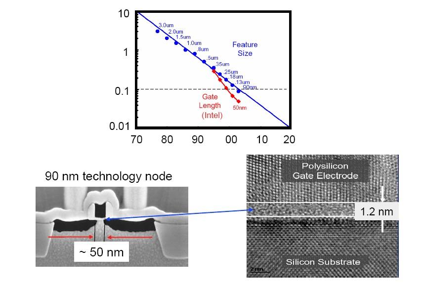
31 2000 Nano Electronics started. Device: Still, Si CMOS integrated circuits Device feature size: 100 nm Major Appl.: Digital (µ processor, cell phone, etc.) Technology Revolution?? Maybe, just evolution and innovation! But great evolution or innovations! and so many innovations!
32 Now, 2014 Nano Electronics continued. Device: Still, Si CMOS integrated circuits Device feature size: around 10 nm Major Appl.: Still Digital (µ processor, cell phone, etc.) Still evolution and innovation.
33
34 Goal: 1TIPS by Pentium 4 Architecture Pentium Pro Architecture MIPS 1000 Pentium Architecture How do you get there? INTEL
35 Technology Scaling SOURCE Xj GATE DRAIN SOURCE GATE BODY DRAIN D Tox BODY Leff Dimensions scale down by Doubles transistor density 30% Oxide thickness scales down Faster transistor, higher performance Vdd & Vt scaling Lower active power Technology has scaled well, will it in the future?

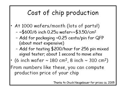
36 Scaling Evolution Iwai Hiroshi

37 MICRO to NANO Journey Milestones J.L.Hoyt MIT
38 Scaling: Importance of Downsizing Downsizing: Capacitance reduction High integration Power reduction Speed increase Function increase Parallel processing Speed increase Iwai Hiroshi
39 Demand for future VLSI: Much higher performance Much lower power consumption Thus, downsizing of Si devices is the most important and critical issue. Iwai Hiroshi
40 Prediction of Scaling limit Vacuum tube era even µm size could not be imagined Since Si IC started Period Expected Cause limit(size) Late 1970 s Early 1980 s Early 1980 s Late 1980 s Today Today 1µm: 0.5µm: 0.25µm: 0.1µm: SCE S/D resistance Direct-tunneling of gate SiO2 0.1µm brick wall (various) 50nm: Red brick wall (various) 10nm: Fundamental?
41 Transistor Integration Capacity Transistors (Million) Billion Technology (µ ) On track for 1B transistor integration capacity INTEL

42 J.L.Hoyt MIT
43 Limits of Moore s Law? Growth expected until 30 nm gate length (currently: 180 nm) size halved every 18 mos. - reached in log2((180/30)2) = 2009 what then? Paradigm shift needed in fabrication process
44 Technological Background of the Moore s Law To accommodate this change, the size of the silicon wafers on which the integrated circuits are fabricated have also increased by a very significant factor from the 2 and 3 in diameter wafers to the 8 in (200 mm) and 12 in (300 mm) diameter wafers The latest catch phrase in semiconductor technology (as well as in other material science) is nanotechnology usually referring to GaAs devices based on quantum mechanical phenomena These devices have feature size (such as film thickness, line width etc) measured in nanometres or 10-9 metres
45 Recurring Costs Variable Cost = {Cost of (Die + Die test + packaging)}/ Final Test Yield Cost of Die = {Cost of wafer}/[ Dies per wafer x Die Yield] x [wafer diameter/2] 2 x wafer diameter Die per wafer = Die area x Die area Die yield= [1 + (defects per unit area x Die area)/α ] α
46 Yield Example Example wafer size of 12 inches, die size of 2.5 cm2, 1 defects/cm2, α = 3 (measure of manufacturing process complexity) 252 dies/wafer (remember, wafers round & dies square) die yield of 16% 252 x 16% = only 40 dies/wafer die yield! Die cost is strong function of die area proportional to the third or fourth power of the die area
47
48
49 PROCESS STEPS
50 Is Transistor a Good Switch? I=0 I 0 On I = 1ma/u I= I=0 I 0 Off I=0 I 0 Sub-threshold Leakage
Transistor was first invented by William.B.Shockley, Walter Brattain and John Bardeen of Bell Labratories. In 1961, first IC was introduced.
 Unit 1 Basic MOS Technology Transistor was first invented by William.B.Shockley, Walter Brattain and John Bardeen of Bell Labratories. In 1961, first IC was introduced. Levels of Integration:- i) SSI:-
VLSI Design. Introduction
 VLSI Design Introduction Outline Introduction Silicon, pn-junctions and transistors A Brief History Operation of MOS Transistors CMOS circuits Fabrication steps for CMOS circuits Introduction Integrated
VLSI Design. Introduction
 Tassadaq Hussain VLSI Design Introduction Outcome of this course Problem Aims Objectives Outcomes Data Collection Theoretical Model Mathematical Model Validate Development Analysis and Observation Pseudo
Progress due to: Feature size reduction - 0.7X/3 years (Moore s Law). Increasing chip size - 16% per year. Creativity in implementing functions.
. Increasing chip size - 16% per year. Creativity in implementing functions.") Introduction - Chapter 1 Evolution of IC Fabrication 1960 and 1990 integrated t circuits. it Progress due to: Feature size reduction - 0.7X/3 years (Moore s Law). Increasing chip size - 16% per year. Creativity
Introduction - Chapter 1 Evolution of IC Fabrication 1960 and 1990 integrated t circuits. it Progress due to: Feature size reduction - 0.7X/3 years (Moore s Law). Increasing chip size - 16% per year. Creativity
420 Intro to VLSI Design
 Dept of Electrical and Computer Engineering 420 Intro to VLSI Design Lecture 0: Course Introduction and Overview Valencia M. Joyner Spring 2005 Getting Started Syllabus About the Instructor Labs, Problem
Integrated Circuit Technology (Course Code: EE662) Lecture 1: Introduction
 Lecture 1: Introduction") Indian Institute of Technology Jodhpur, Year 2015 2016 Integrated Circuit Technology (Course Code: EE662) Lecture 1: Introduction Course Instructor: Shree Prakash Tiwari, Ph.D. Email: sptiwari@iitj.ac.in
Indian Institute of Technology Jodhpur, Year 2015 2016 Integrated Circuit Technology (Course Code: EE662) Lecture 1: Introduction Course Instructor: Shree Prakash Tiwari, Ph.D. Email: sptiwari@iitj.ac.in
EMT 251 Introduction to IC Design
 EMT 251 Introduction to IC Design (Pengantar Rekabentuk Litar Terkamir) Semester II 2011/2012 Introduction to IC design and Transistor Fundamental Some Keywords! Very-large-scale-integration (VLSI) is
EE4800 CMOS Digital IC Design & Analysis. Lecture 1 Introduction Zhuo Feng
 EE4800 CMOS Digital IC Design & Analysis Lecture 1 Introduction Zhuo Feng 1.1 Prof. Zhuo Feng Office: EERC 730 Phone: 487-3116 Email: zhuofeng@mtu.edu Class Website http://www.ece.mtu.edu/~zhuofeng/ee4800fall2010.html
Digital Integrated Circuits
 Digital Integrated Circuits Yaping Dan ( 但亚平 ), PhD Office: Law School North 301 Tel: 34206045-3011 Email: yapingd@gmail.com Digital Integrated Circuits Introduction p-n junctions and MOSFETs The CMOS
Lecture Integrated circuits era
 Lecture 1 1.1 Integrated circuits era Transistor was first invented by William.B.Shockley, Walter Brattain and John Bardeen of Bell laboratories. In 1961, first IC was introduced. Levels of Integration:-
Semiconductor Devices
 Semiconductor Devices - 2014 Lecture Course Part of SS Module PY4P03 Dr. P. Stamenov School of Physics and CRANN, Trinity College, Dublin 2, Ireland Hilary Term, TCD 3 th of Feb 14 MOSFET Unmodified Channel
Lecture 0: Introduction
 Lecture 0: Introduction Introduction Integrated circuits: many transistors on one chip. Very Large Scale Integration (VLSI): bucketloads! Complementary Metal Oxide Semiconductor Fast, cheap, low power
VLSI: An Introduction
 Chapter 1 UEEA2223/UEEG4223 Integrated Circuit Design VLSI: An Introduction Prepared by Dr. Lim Soo King 02 Jan 2011. Chapter 1 VLSI Design: An Introduction... 1 1.0 Introduction... 1 1.0.1 Early Computing
Introduction to VLSI ASIC Design and Technology
 Introduction to VLSI ASIC Design and Technology Paulo Moreira CERN - Geneva, Switzerland Paulo Moreira Introduction 1 Outline Introduction Is there a limit? Transistors CMOS building blocks Parasitics
Chapter 1, Introduction
 Introduction to Semiconductor Manufacturing Technology Chapter 1, Introduction hxiao89@hotmail.com 1 Objective After taking this course, you will able to Use common semiconductor terminology Describe a
MICROPROCESSOR TECHNOLOGY
 MICROPROCESSOR TECHNOLOGY Assis. Prof. Hossam El-Din Moustafa Lecture 3 Ch.1 The Evolution of The Microprocessor 17-Feb-15 1 Chapter Objectives Introduce the microprocessor evolution from transistors to
Intel s High-k/Metal Gate Announcement. November 4th, 2003
 Intel s High-k/Metal Gate Announcement November 4th, 2003 1 What are we announcing? Intel has made significant progress in future transistor materials Two key parts of this new transistor are: The gate
CMOS Digital Integrated Circuits Lec 2 Fabrication of MOSFETs
 CMOS Digital Integrated Circuits Lec 2 Fabrication of MOSFETs 1 CMOS Digital Integrated Circuits 3 rd Edition Categories of Materials Materials can be categorized into three main groups regarding their
Lecture #29. Moore s Law
 Lecture #29 ANNOUNCEMENTS HW#15 will be for extra credit Quiz #6 (Thursday 5/8) will include MOSFET C-V No late Projects will be accepted after Thursday 5/8 The last Coffee Hour will be held this Thursday
EE 5611 Introduction to Microelectronic Technologies Fall Thursday, September 04, 2014 Lecture 02
 EE 5611 Introduction to Microelectronic Technologies Fall 2014 Thursday, September 04, 2014 Lecture 02 1 Lecture Outline Review on semiconductor materials Review on microelectronic devices Example of microelectronic
Chapter 3: Basics Semiconductor Devices and Processing 2006/9/27 1. Topics
 Chapter 3: Basics Semiconductor Devices and Processing 2006/9/27 1 Topics What is semiconductor Basic semiconductor devices Basics of IC processing CMOS technologies 2006/9/27 2 1 What is Semiconductor
Lecture 1 Introduction to Solid State Electronics
 EE 471: Transport Phenomena in Solid State Devices Spring 2018 Lecture 1 Introduction to Solid State Electronics Bryan Ackland Department of Electrical and Computer Engineering Stevens Institute of Technology
Integrated diodes. The forward voltage drop only slightly depends on the forward current. ELEKTRONIKOS ĮTAISAI
 1 Integrated diodes pn junctions of transistor structures can be used as integrated diodes. The choice of the junction is limited by the considerations of switching speed and breakdown voltage. The forward
EE 330 Lecture 7. Design Rules. IC Fabrication Technology Part 1
 EE 330 Lecture 7 Design Rules IC Fabrication Technology Part 1 Review from Last Time Technology Files Provide Information About Process Process Flow (Fabrication Technology) Model Parameters Design Rules
IH2655 Design and Characterisation of Nano- and Microdevices. Lecture 1 Introduction and technology roadmap
 IH2655 Design and Characterisation of Nano- and Microdevices Lecture 1 Introduction and technology roadmap IH2655 Design and Characterisation of Nano- and Microdevices Introduction to IH2655 Brief historic
Selected Topics in Nanoelectronics. Danny Porath 2002
 Selected Topics in Nanoelectronics Danny Porath 2002 Links to NST http://www.foresight.org/ http://itri.loyola.edu/nanobase/ http://www.zyvex.com/nano/ http://www.nano.gov/ http://www.aeiveos.com/nanotech/
+1 (479)
") Introduction to VLSI Design http://csce.uark.edu +1 (479) 575-6043 yrpeng@uark.edu Invention of the Transistor Vacuum tubes ruled in first half of 20th century Large, expensive, power-hungry, unreliable
Introduction to VLSI Design http://csce.uark.edu +1 (479) 575-6043 yrpeng@uark.edu Invention of the Transistor Vacuum tubes ruled in first half of 20th century Large, expensive, power-hungry, unreliable
ATV 2011: Computer Engineering
 ATV 2011: Technology Trends in Computer Engineering Professor Per Larsson-Edefors ATV 2011, L1, Per Larsson-Edefors Page 1 Solid-State Devices www.cse.chalmers.se/~perla/ugrad/ SemTech/Lectures_2000.pdf
Design Simulation and Analysis of NMOS Characteristics for Varying Oxide Thickness
 MIT International Journal of Electronics and Communication Engineering, Vol. 4, No. 2, August 2014, pp. 81 85 81 Design Simulation and Analysis of NMOS Characteristics for Varying Oxide Thickness Alpana
Topic 3. CMOS Fabrication Process
 Topic 3 CMOS Fabrication Process Peter Cheung Department of Electrical & Electronic Engineering Imperial College London URL: www.ee.ic.ac.uk/pcheung/ E-mail: p.cheung@ic.ac.uk Lecture 3-1 Layout of a Inverter
Chapter 15 Summary and Future Trends
 Chapter 15 Summary and Future Trends Hong Xiao, Ph. D. hxiao89@hotmail.com www2.austin.cc.tx.us/hongxiao/book.htm Hong Xiao, Ph. D. www2.austin.cc.tx.us/hongxiao/book.htm 1 The 1960s First IC product Bipolar
In this lecture we will begin a new topic namely the Metal-Oxide-Semiconductor Field Effect Transistor.
 Solid State Devices Dr. S. Karmalkar Department of Electronics and Communication Engineering Indian Institute of Technology, Madras Lecture - 38 MOS Field Effect Transistor In this lecture we will begin
Chapter 3 Basics Semiconductor Devices and Processing
 Chapter 3 Basics Semiconductor Devices and Processing 1 Objectives Identify at least two semiconductor materials from the periodic table of elements List n-type and p-type dopants Describe a diode and
EE 410: Integrated Circuit Fabrication Laboratory
 EE 410: Integrated Circuit Fabrication Laboratory 1 EE 410: Integrated Circuit Fabrication Laboratory Web Site: Instructor: http://www.stanford.edu/class/ee410 https://ccnet.stanford.edu/ee410/ (on CCNET)
Notes. (Subject Code: 7EC5)
") COMPUCOM INSTITUTE OF TECHNOLOGY & MANAGEMENT, JAIPUR (DEPARTMENT OF ELECTRONICS & COMMUNICATION) Notes VLSI DESIGN NOTES (Subject Code: 7EC5) Prepared By: MANVENDRA SINGH Class: B. Tech. IV Year, VII
COMPUCOM INSTITUTE OF TECHNOLOGY & MANAGEMENT, JAIPUR (DEPARTMENT OF ELECTRONICS & COMMUNICATION) Notes VLSI DESIGN NOTES (Subject Code: 7EC5) Prepared By: MANVENDRA SINGH Class: B. Tech. IV Year, VII
In 1951 William Shockley developed the world first junction transistor. One year later Geoffrey W. A. Dummer published the concept of the integrated
 Objectives History and road map of integrated circuits Application specific integrated circuits Design flow and tasks Electric design automation tools ASIC project MSDAP In 1951 William Shockley developed
Introduction. Digital Integrated Circuits A Design Perspective. Jan M. Rabaey Anantha Chandrakasan Borivoje Nikolic. July 30, 2002
 Digital Integrated Circuits A Design Perspective Jan M. Rabaey Anantha Chandrakasan Borivoje Nikolic Introduction July 30, 2002 1 What is this book all about? Introduction to digital integrated circuits.
ECE520 VLSI Design. Lecture 2: Basic MOS Physics. Payman Zarkesh-Ha
 ECE520 VLSI Design Lecture 2: Basic MOS Physics Payman Zarkesh-Ha Office: ECE Bldg. 230B Office hours: Wednesday 2:00-3:00PM or by appointment E-mail: pzarkesh@unm.edu Slide: 1 Review of Last Lecture Semiconductor
Introduction to Electronic Devices
 (Course Number 300331) Fall 2006 Instructor: Dr. Dietmar Knipp Assistant Professor of Electrical Engineering Information: http://www.faculty.iubremen.de/dknipp/ Source: Apple Ref.: Apple Ref.: IBM Critical
Semiconductor Physics and Devices
 Metal-Semiconductor and Semiconductor Heterojunctions The Metal-Oxide-Semiconductor Field-Effect Transistor (MOSFET) is one of two major types of transistors. The MOSFET is used in digital circuit, because
ECE 484 VLSI Digital Circuits Fall Lecture 02: Design Metrics
 ECE 484 VLSI Digital Circuits Fall 2016 Lecture 02: Design Metrics Dr. George L. Engel Adapted from slides provided by Mary Jane Irwin (PSU) [Adapted from Rabaey s Digital Integrated Circuits, 2002, J.
Layout of a Inverter. Topic 3. CMOS Fabrication Process. The CMOS Process - photolithography (2) The CMOS Process - photolithography (1) v o.
 The CMOS Process - photolithography (1) v o.") Layout of a Inverter Topic 3 CMOS Fabrication Process V DD Q p Peter Cheung Department of Electrical & Electronic Engineering Imperial College London v i v o Q n URL: www.ee.ic.ac.uk/pcheung/ E-mail: p.cheung@ic.ac.uk
Layout of a Inverter Topic 3 CMOS Fabrication Process V DD Q p Peter Cheung Department of Electrical & Electronic Engineering Imperial College London v i v o Q n URL: www.ee.ic.ac.uk/pcheung/ E-mail: p.cheung@ic.ac.uk
EECS 151/251A Spring 2019 Digital Design and Integrated Circuits. Instructors: Wawrzynek. Lecture 8 EE141
 EECS 151/251A Spring 2019 Digital Design and Integrated Circuits Instructors: Wawrzynek Lecture 8 EE141 From the Bottom Up IC processing CMOS Circuits (next lecture) EE141 2 Overview of Physical Implementations
Quantum Condensed Matter Physics Lecture 16
 Quantum Condensed Matter Physics Lecture 16 David Ritchie QCMP Lent/Easter 2018 http://www.sp.phy.cam.ac.uk/drp2/home 16.1 Quantum Condensed Matter Physics 1. Classical and Semi-classical models for electrons
FABRICATION OF CMOS INTEGRATED CIRCUITS. Dr. Mohammed M. Farag
 FABRICATION OF CMOS INTEGRATED CIRCUITS Dr. Mohammed M. Farag Outline Overview of CMOS Fabrication Processes The CMOS Fabrication Process Flow Design Rules Reference: Uyemura, John P. "Introduction to
2.8 - CMOS TECHNOLOGY
 CMOS Technology (6/7/00) Page 1 2.8 - CMOS TECHNOLOGY INTRODUCTION Objective The objective of this presentation is: 1.) Illustrate the fabrication sequence for a typical MOS transistor 2.) Show the physical
MOSFET & IC Basics - GATE Problems (Part - I)
") MOSFET & IC Basics - GATE Problems (Part - I) 1. Channel current is reduced on application of a more positive voltage to the GATE of the depletion mode n channel MOSFET. (True/False) [GATE 1994: 1 Mark]
MOSFET & IC Basics - GATE Problems (Part - I) 1. Channel current is reduced on application of a more positive voltage to the GATE of the depletion mode n channel MOSFET. (True/False) [GATE 1994: 1 Mark]
Lecture: Integration of silicon photonics with electronics. Prepared by Jean-Marc FEDELI CEA-LETI
 Lecture: Integration of silicon photonics with electronics Prepared by Jean-Marc FEDELI CEA-LETI Context The goal is to give optical functionalities to electronics integrated circuit (EIC) The objectives
Lecture 33 - The Short Metal-Oxide-Semiconductor Field-Effect Transistor (cont.) April 30, 2007
 April 30, 2007") 6.720J/3.43J - Integrated Microelectronic Devices - Spring 2007 Lecture 33-1 Lecture 33 - The Short Metal-Oxide-Semiconductor Field-Effect Transistor (cont.) April 30, 2007 Contents: 1. MOSFET scaling
6.720J/3.43J - Integrated Microelectronic Devices - Spring 2007 Lecture 33-1 Lecture 33 - The Short Metal-Oxide-Semiconductor Field-Effect Transistor (cont.) April 30, 2007 Contents: 1. MOSFET scaling
Introduction to Materials Engineering: Materials Driving the Electronics Revolution Robert Hull, MSE
 Introduction to Materials Engineering: Materials Driving the Electronics Revolution Robert Hull, MSE Outline Microelectronics Miniaturization Historical Development: Electronics before Semiconductors The
Lecture Wrap up. December 13, 2005
 6.012 Microelectronic Devices and Circuits Fall 2005 Lecture 26 1 Lecture 26 6.012 Wrap up December 13, 2005 Contents: 1. 6.012 wrap up Announcements: Final exam TA review session: December 16, 7:30 9:30
Parameter Optimization Of GAA Nano Wire FET Using Taguchi Method
 Parameter Optimization Of GAA Nano Wire FET Using Taguchi Method S.P. Venu Madhava Rao E.V.L.N Rangacharyulu K.Lal Kishore Professor, SNIST Professor, PSMCET Registrar, JNTUH Abstract As the process technology
LSI ON GLASS SUBSTRATES
 LSI ON GLASS SUBSTRATES OUTLINE Introduction: Why System on Glass? MOSFET Technology Low-Temperature Poly-Si TFT Technology System-on-Glass Technology Issues Conclusion System on Glass CPU SRAM DRAM EEPROM
1 Digital EE141 Integrated Circuits 2nd Introduction
 Digital Integrated Circuits Introduction 1 What is this lecture about? Introduction to digital integrated circuits + low power circuits Issues in digital design The CMOS inverter Combinational logic structures
32nm High-K/Metal Gate Version Including 2nd Generation Intel Core processor family
 From Sand to Silicon Making of a Chip Illustrations 32nm High-K/Metal Gate Version Including 2nd Generation Intel Core processor family April 2011 1 The illustrations on the following foils are low resolution
Semiconductor Devices
 Semiconductor Devices Modelling and Technology Source Electrons Gate Holes Drain Insulator Nandita DasGupta Amitava DasGupta SEMICONDUCTOR DEVICES Modelling and Technology NANDITA DASGUPTA Professor Department
Part II: The MOS Transistor Technology. J. SÉE 2004/2005
 Part II: The MOS Transistor Technology J. SÉE johann.see@ief.u-psud.fr 2004/2005 Lecture plan Towards the nanotechnologies... data storage The data processing through the ages MOS transistor in logic-gates
6.012 Microelectronic Devices and Circuits
 MIT, Spring 2009 6.012 Microelectronic Devices and Circuits Charles G. Sodini Jing Kong Shaya Famini, Stephanie Hsu, Ming Tang Lecture 1 6.012 Overview Contents: Overview of 6.012 Reading Assignment: Howe
6.012 Microelectronic Devices and Circuits
 MIT, Spring 2003 6.012 Microelectronic Devices and Circuits Jesús del Alamo Dimitri Antoniadis, Judy Hoyt, Charles Sodini Pablo Acosta, Susan Luschas, Jorg Scholvin, Niamh Waldron Lecture 1 6.012 overview
Silicon VLSI Technology. Fundamentals, Practice and Modeling. Class Notes For Instructors. J. D. Plummer, M. D. Deal and P. B.
 Silicon VLSI Technology Fundamentals, ractice, and Modeling Class otes For Instructors J. D. lummer, M. D. Deal and. B. Griffin These notes are intended to be used for lectures based on the above text.
ECE 5745 Complex Digital ASIC Design Topic 2: CMOS Devices
 ECE 5745 Complex Digital ASIC Design Topic 2: CMOS Devices Christopher Batten School of Electrical and Computer Engineering Cornell University http://www.csl.cornell.edu/courses/ece5950 Simple Transistor
Sub-micron technology IC fabrication process trends SOI technology. Development of CMOS technology. Technology problems due to scaling
 Goodbye Microelectronics Welcome Nanoelectronics Sub-micron technology IC fabrication process trends SOI technology SiGe Tranzistor in 50nm process Virus The thickness of gate oxide= 1.2 nm!!! Today we
Past and future for micro- and nano-electronics, focusing on Si integrated circuits technology
 Past and future for micro- and nano-electronics, focusing on Si integrated circuits technology June 2, 2008 @National Technical University of Athens Hiroshi Iwai, Toyo Institute of Technology Needless
Design and Analysis of Double Gate MOSFET Devices using High-k Dielectric
 International Journal of Electrical Engineering. ISSN 0974-2158 Volume 7, Number 1 (2014), pp. 53-60 International Research Publication House http://www.irphouse.com Design and Analysis of Double Gate
Practical Information
 EE241 - Spring 2013 Advanced Digital Integrated Circuits MW 2-3:30pm 540A/B Cory Practical Information Instructor: Borivoje Nikolić 509 Cory Hall, 3-9297, bora@eecs Office hours: M 11-12, W 3:30pm-4:30pm
SRM INSTITUTE OF SCIENCE AND TECHNOLOGY (DEEMED UNIVERSITY)
") SRM INSTITUTE OF SCIENCE AND TECHNOLOGY (DEEMED UNIVERSITY) QUESTION BANK I YEAR B.Tech (II Semester) ELECTRONIC DEVICES (COMMON FOR EC102, EE104, IC108, BM106) UNIT-I PART-A 1. What are intrinsic and
SRM INSTITUTE OF SCIENCE AND TECHNOLOGY (DEEMED UNIVERSITY) QUESTION BANK I YEAR B.Tech (II Semester) ELECTRONIC DEVICES (COMMON FOR EC102, EE104, IC108, BM106) UNIT-I PART-A 1. What are intrinsic and
ECE-606: Spring Course Introduction
 ECE-606: Spring 2013 Course Introduction Professor Mark Lundstrom Electrical and Computer Engineering Purdue University, West Lafayette, IN USA lundstro@purdue.edu 1/8/13 1 course objectives To introduce
Chapter 2 : Semiconductor Materials & Devices (II) Feb
 Feb") Chapter 2 : Semiconductor Materials & Devices (II) 1 Reference 1. SemiconductorManufacturing Technology: Michael Quirk and Julian Serda (2001) 3. Microelectronic Circuits (5/e): Sedra & Smith (2004) 4.
Chapter 2 : Semiconductor Materials & Devices (II) 1 Reference 1. SemiconductorManufacturing Technology: Michael Quirk and Julian Serda (2001) 3. Microelectronic Circuits (5/e): Sedra & Smith (2004) 4.
Session 3: Solid State Devices. Silicon on Insulator
 Session 3: Solid State Devices Silicon on Insulator 1 Outline A B C D E F G H I J 2 Outline Ref: Taurand Ning 3 SOI Technology SOl materials: SIMOX, BESOl, and Smart Cut SIMOX : Synthesis by IMplanted
Advanced Digital Integrated Circuits. Lecture 2: Scaling Trends. Announcements. No office hour next Monday. Extra office hour Tuesday 2-3pm
 EE241 - Spring 20 Advanced Digital Integrated Circuits Lecture 2: Scaling Trends and Features of Modern Technologies Announcements No office hour next Monday Extra office hour Tuesday 2-3pm 2 1 Outline
2014, IJARCSSE All Rights Reserved Page 1352
 Volume 4, Issue 3, March 2014 ISSN: 2277 128X International Journal of Advanced Research in Computer Science and Software Engineering Research Paper Available online at: www.ijarcsse.com Double Gate N-MOSFET
Semiconductor Memory: DRAM and SRAM. Department of Electrical and Computer Engineering, National University of Singapore
 Semiconductor Memory: DRAM and SRAM Outline Introduction Random Access Memory (RAM) DRAM SRAM Non-volatile memory UV EPROM EEPROM Flash memory SONOS memory QD memory Introduction Slow memories Magnetic
DIGITAL TECHNICS II. Dr. Bálint Pődör. Óbuda University, Microelectronics and Technology Institute 6. LECTURE: LOGIC CIRCUITS I
 DIGITAL TECHNICS II Dr. Bálint Pődör Óbuda University, Microelectronics and Technology Institute 6. LECTURE: LOGIC CIRCUITS I 1st (Spring) term 2015/2016 1 6. LECTURE LOGIC CIRCUITS I 1. Digital/logic
UNIT III VLSI CIRCUIT DESIGN PROCESSES. In this chapter we will be studying how to get the schematic into stick diagrams or layouts.
 UNIT III VLSI CIRCUIT DESIGN PROCESSES In this chapter we will be studying how to get the schematic into stick diagrams or layouts. MOS circuits are formed on four basic layers: N-diffusion P-diffusion
Introduction to Microdevices and Microsystems
 PHYS 534 (Fall 2008) Module on Microsystems & Microfabrication Lecture 1 Introduction to Microdevices and Microsystems Srikar Vengallatore, McGill University 1 Introduction to Microsystems Outline of Lecture
Lecture 020 ECE4430 Review II (1/5/04) Page 020-1
 Page 020-1") Lecture 020 ECE4430 Review II (1/5/04) Page 020-1 LECTURE 020 ECE 4430 REVIEW II (READING: GHLM - Chap. 2) Objective The objective of this presentation is: 1.) Identify the prerequisite material as taught
Lecture 020 ECE4430 Review II (1/5/04) Page 020-1 LECTURE 020 ECE 4430 REVIEW II (READING: GHLM - Chap. 2) Objective The objective of this presentation is: 1.) Identify the prerequisite material as taught
Challenges and Innovations in Nano CMOS Transistor Scaling
 Challenges and Innovations in Nano CMOS Transistor Scaling Tahir Ghani Intel Fellow Logic Technology Development October, 2009 Nikkei Presentation 1 Outline Traditional Scaling Traditional Scaling Limiters,
The future of lithography and its impact on design
 The future of lithography and its impact on design Chris Mack www.lithoguru.com 1 Outline History Lessons Moore s Law Dennard Scaling Cost Trends Is Moore s Law Over? Litho scaling? The Design Gap The
Lecture 1, Introduction and Background
 EE 338L CMOS Analog Integrated Circuit Design Lecture 1, Introduction and Background With the advances of VLSI (very large scale integration) technology, digital signal processing is proliferating and
Future Challenges and Needs for Nano- Electronics from Manufacturing View Point
 First International Symposium on Nano-manufacturing, April 24-26, 2003 Future Challenges and Needs for Nano- Electronics from Manufacturing View Point Yoshio Nishi Stanford Nanofabrication Facility Department
Solid State Devices- Part- II. Module- IV
 Solid State Devices- Part- II Module- IV MOS Capacitor Two terminal MOS device MOS = Metal- Oxide- Semiconductor MOS capacitor - the heart of the MOSFET The MOS capacitor is used to induce charge at the
Future MOSFET Devices using high-k (TiO 2 ) dielectric
 dielectric") Future MOSFET Devices using high-k (TiO 2 ) dielectric Prerna Guru Jambheshwar University, G.J.U.S. & T., Hisar, Haryana, India, prernaa.29@gmail.com Abstract: In this paper, an 80nm NMOS with high-k (TiO
Future MOSFET Devices using high-k (TiO 2 ) dielectric Prerna Guru Jambheshwar University, G.J.U.S. & T., Hisar, Haryana, India, prernaa.29@gmail.com Abstract: In this paper, an 80nm NMOS with high-k (TiO
EECS130 Integrated Circuit Devices
 EECS130 Integrated Circuit Devices Professor Ali Javey 11/01/2007 MOSFETs Lecture 5 Announcements HW7 set is due now HW8 is assigned, but will not be collected/graded. MOSFET Technology Scaling Technology
Jan M. Rabaey Anantha Chandrakasan Borivoje Nikolic. July 30, Digital EE141 Integrated Circuits 2nd Introduction
 Digital Integrated Circuits A Design Perspective Jan M. Rabaey Anantha Chandrakasan Borivoje Nikolic Introduction July 30, 2002 1 What is this book all about? Introduction to digital integrated circuits.
FOUNDRY SERVICE. SEI's FEATURE. Wireless Devices FOUNDRY SERVICE. SRD-800DD, SRD-500DD D-FET Process Lg=0.8, 0.5µm. Ion Implanted MESFETs SRD-301ED
 FOUNDRY SERVICE 01.04. Foundry services have been one of the core businesses at SEI, providing sophisticated GaAs IC technology for all customers. SEI offers very flexible service to support the customers
EE 330 Lecture 11. Capacitances in Interconnects Back-end Processing
 EE 330 Lecture 11 Capacitances in Interconnects Back-end Processing Exam 1 Friday Sept 21 Students may bring 1 page of notes HW assignment for week of Sept 16 due on Wed Sept 19 at beginning of class No
Alternatives to standard MOSFETs. What problems are we really trying to solve?
 Alternatives to standard MOSFETs A number of alternative FET schemes have been proposed, with an eye toward scaling up to the 10 nm node. Modifications to the standard MOSFET include: Silicon-in-insulator
This Week s Subject. DRAM & Flexible RRAM. p-channel MOSFET (PMOS) CMOS: Complementary Metal Oxide Semiconductor
 CMOS: Complementary Metal Oxide Semiconductor") DRAM & Flexible RRAM This Week s Subject p-channel MOSFET (PMOS) CMOS: Complementary Metal Oxide Semiconductor CMOS Logic Inverter NAND gate NOR gate CMOS Integration & Layout GaAs MESFET (JFET) 1 Flexible
DRAM & Flexible RRAM This Week s Subject p-channel MOSFET (PMOS) CMOS: Complementary Metal Oxide Semiconductor CMOS Logic Inverter NAND gate NOR gate CMOS Integration & Layout GaAs MESFET (JFET) 1 Flexible
Design cycle for MEMS
 Design cycle for MEMS Design cycle for ICs IC Process Selection nmos CMOS BiCMOS ECL for logic for I/O and driver circuit for critical high speed parts of the system The Real Estate of a Wafer MOS Transistor
Silicon on Insulator (SOI) Spring 2018 EE 532 Tao Chen
 Spring 2018 EE 532 Tao Chen") Silicon on Insulator (SOI) Spring 2018 EE 532 Tao Chen What is Silicon on Insulator (SOI)? SOI silicon on insulator, refers to placing a thin layer of silicon on top of an insulator such as SiO2. The devices
Silicon on Insulator (SOI) Spring 2018 EE 532 Tao Chen What is Silicon on Insulator (SOI)? SOI silicon on insulator, refers to placing a thin layer of silicon on top of an insulator such as SiO2. The devices
ECEN474: (Analog) VLSI Circuit Design Fall 2011
 VLSI Circuit Design Fall 2011") ECEN474: (Analog) VLSI Circuit Design Fall 2011 Lecture 1: Introduction Sebastian Hoyos Analog & Mixed-Signal Center Texas A&M University Analog Circuit Sequence 326 2 Why is Analog Important? [Silva]
ECEN474: (Analog) VLSI Circuit Design Fall 2011 Lecture 1: Introduction Sebastian Hoyos Analog & Mixed-Signal Center Texas A&M University Analog Circuit Sequence 326 2 Why is Analog Important? [Silva]
Organic Electronics. Information: Information: 0331a/ 0442/
 Organic Electronics (Course Number 300442 ) Spring 2006 Organic Field Effect Transistors Instructor: Dr. Dietmar Knipp Information: Information: http://www.faculty.iubremen.de/course/c30 http://www.faculty.iubremen.de/course/c30
Atomic-layer deposition of ultrathin gate dielectrics and Si new functional devices
 Atomic-layer deposition of ultrathin gate dielectrics and Si new functional devices Anri Nakajima Research Center for Nanodevices and Systems, Hiroshima University 1-4-2 Kagamiyama, Higashi-Hiroshima,
CPE/EE 427, CPE 527 VLSI Design I L01: Introduction, Design Metrics. What is this course all about?
 CPE/EE 427, CPE 527 VLSI Design I L01: Introduction, Design Metrics Aleksandar Milenkovic ( www.ece.uah.edu/~milenka ) www.ece.uah.edu/~milenka/cpe527-05f What is this course all about? Introduction to
FUNDAMENTALS OF MODERN VLSI DEVICES
 19-13- FUNDAMENTALS OF MODERN VLSI DEVICES YUAN TAUR TAK H. MING CAMBRIDGE UNIVERSITY PRESS Physical Constants and Unit Conversions List of Symbols Preface page xi xiii xxi 1 INTRODUCTION I 1.1 Evolution
40nm Node CMOS Platform UX8
 FUKAI Toshinori, IKEDA Masahiro, TAKAHASHI Toshifumi, NATSUME Hidetaka Abstract The UX8 is the latest process from NEC Electronics. It uses the most advanced exposure technology to achieve twice the gate
VLSI Design I; A. Milenkovic 1
 CPE/EE 427, CPE 527 VLSI Design I L02: Design Metrics Department of Electrical and Computer Engineering University of Alabama in Huntsville Aleksandar Milenkovic ( www.ece.uah.edu/~milenka ) www.ece.uah.edu/~milenka/cpe527-03f
Introduction. Introduction. Digital Integrated Circuits A Design Perspective. Introduction. The First Computer
 Digital Integrated Circuits A Design Perspective Prentice Hall Electronics and VLSI Series ISBN 0-3-20764-4 [Adapted from Rabaey s Digital Integrated Circuits, Second Edition, 2003 J. Rabaey, A. Chandrakasan,
ITRS MOSFET Scaling Trends, Challenges, and Key Technology Innovations
 Workshop on Frontiers of Extreme Computing Santa Cruz, CA October 24, 2005 ITRS MOSFET Scaling Trends, Challenges, and Key Technology Innovations Peter M. Zeitzoff Outline Introduction MOSFET scaling and