Chapter 2 : Semiconductor Materials & Devices (II) Feb
|
|
|
- Ophelia Sullivan
- 5 years ago
- Views:
Transcription
1 Chapter 2 : Semiconductor Materials & Devices (II) 1
2 Reference 1. SemiconductorManufacturing Technology: Michael Quirk and Julian Serda (2001) 3. Microelectronic Circuits (5/e): Sedra & Smith (2004) 4. Semiconductor Physics and Devices- Basic Principles (3/e) : Donald A. Neamen (2003) 5. Semiconductor Devices - Physics and Technology (2/e) : S. M. Sze (2002) 2

3 Bipolar Junction Transistor 3

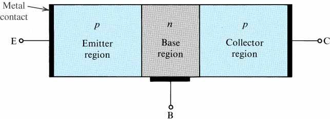
4 Cross Section of an NPN BJT BJT is not a symmetrical device and the impurity doping concentrations in the emitter and collector are different. 4

5 NPN Transistor Biasing Circuit 5 Current flow in an npn transistor biased to operate in the active mode. (Reverse current components due to drift of thermally generated minority carriers are not shown.)

6 PNP transistor biasing circuit 6 Current flow in a pnp transistor biased to operate in the active mode.
7 The Transistor Action (a) Idealized one-dimensional schematic of a p-n-p bipolar transistor and (b) its circuit symbol. (c) Idealized one-dimensional schematic of an n-p-n bipolar transistor (d) its circuit symbol. 7
8 Modes of Operation Junction polarities and minority carrier distributions of a p-n-p transistor under four modes of operation. 8
9 Operation in the Thermal Equilibrium (a) A p-n-p transistor with all leads grounded (at thermal equilibrium). (b) Doping profile of a transistor with abrupt impurity distributions. (c) Electric-field profile. (d) Energy band diagram at thermal equilibrium. 9
10 Operation in the Active Mode Common-base (CB) configuration (a) The transistor under the active mode of operation. (b) Doping profiles and the depletion regions under biasing conditions. (c) Electric-field profile. (d) Energy band diagram. 10

11 I I I E C B = I = I = I = I Ep Cp E En + I + I I C + ( I En Cn Ep I Cp ) I Cn Current Gain Common-base configuration common- base current gain I Cp I Ep I Cp α 0 = = I Ep + I En I Ep I En I + Ep = γαt γ : emitter eff. αt : base transport factor I = I + I = α I + I C Cp = α I 0 E Cn + I CBO T Ep α 0 Cn I I Cp E I EP -I CP =I BB Various current components in a p-n-p transistor under active mode of operation. The electron flow is in the opposite 11 direction to the electron current. = I CBO
12 Current-Voltage Characteristics Common-base configuration (a) Common-base configuration of a p-n-p transistor. 12 (b) Its output current-voltage characteristics.
13 13
14 CE CC CB CE CC CB V i V o
15 Applications Advantage High operating speed High driving current Analog Circuits Amplifier RF circuits Automobile electronics 15
16 Bipolar Logic Family Bipolar Logic Families Table 3.1 Bipolar Logic Families Abbreviation Direct-Coupled Transistor Logic DCTL 1 Resistor-Transistor Logic RTL 2 Resistor-Capacitor-Transistor Logic RCTL 3 Diode-Transistor Logic DTL 4 Transistor-Transistor Logic* TTL 5 Schottky TTL Logic* STTL 6 Emitter-Coupled Logic* ECL 7 1 G. Deboo and C. Burrous, Integrated Circuits and Semiconductor Devices: Theory and Application, 2 nd edition, McGraw-Hill, New York, NY, 1977, p G. Deboo and C. Burrous, ibid. 3 G. Deboo and C. Burrous, ibid. 4 G. Deboo and C. Burrous, ibid. 5 G. Deboo and C. Burrous, ibid. 6 A. Sedra, Feb. K Smith, Microelectronic Circuits, Oxford University Press, 1998, p A. Sedra, K. Smith, Microelectronic Circuits, Oxford University Press, 1998, p
17 Metal-Oxide-Semiconductor Field-Effect Transistor (MOSFET) Size comparison of a wafer to individual components. (a) Semiconductor wafer. (b) Chip. (c) MOSFET and bipolar transistor. 17

 Lightly doped")
18 Gate Structure of MOSFET Metal (Aluminum) polysilicon Oxide thickness of tox Source and Drain Two heavily doped regions Body or substrate ( bulk or body ) Lightly doped substrate 18
 perspective view; (b)")
 is")
19 Structure of MOSFET Physical structure of the enhancement-type NMOS transistor: (a) perspective view; (b) cross-section. Typically L = 0.1 to 3 mm, W = 0.2 to 100 mm, and the thickness of the oxide layer (t ox ) is in the range of 2 to 50 nm. 19

20 Mechanism of MOSFET The enhancement-type NMOS transistor with a positive voltage applied to the gate. An n channel is induced at the top of the substrate beneath the gate. 20

21 Mechanism of MOSFET An NMOS transistor with v GS > V t and with a small v DS applied. The device acts as a resistance whose value is determined by v GS. Specifically, the channel conductance is proportional to v GS V t and thus i D is proportional to (v GS V t ) v DS. 21

22 Mechanism of MOSFET Operation of the enhancement NMOS transistor as v DS is increased. The induced channel Feb. acquires 2005 a tapered shape, and its resistance increases as v DS is increased. Here, v 22 GS is kept constant at a value > V t.
23 Mechanism of MOSFET Threshold volatge 2 S qn A (2φ fn + V BS ) V T V FB + 2φ fn + ; φ fn = C o kt q ln( N n i A ) The drain Feb. current 2005 i D versus the drain-to-source voltage v DS for an enhancementtype NMOS transistor operated with v 23 GS > V t.
24 Current-Voltage Relationship Family of I D versus V DS curves for an n- channel enhancement-mode MOSFET Family of I D versus V DS curves for an n-channel depletion-mode MOSFET I I D = = Wµ nc 2L Wµ nc 2L ox ox [2( V ( V GS V V ) T 2 ) V DS (in V 2 DS ] (in non - saturation region) saturation region) D GS T 24

25 N-channel Metal-Oxide-Semiconductor Gate poly Source, Drain n-type Substrate p-type Carrier electrons 25
26 P-channel Metal-Oxide-Semiconductor Gate poly Source, Drain p-type Substrate n-type Carrier holes 26
 for PMOS Advantage High input impedance Low")
27 Complementary MOS (CMOS) NMOS + PMOS Local substrate (n-well) for PMOS Advantage High input impedance Low power 27
28 Comparison of Enhancement and Depletion Mode MOSFETs 28
29 NMOS Fabrication Processes-(I) Cross-sectional view of NMOS fabrication sequence. (a) Formation of SiO 2, Si 3 N 4, and photoresist layer. (b) Boron implant. (c) Field oxide. (d) Gate. 29
30 NMOS Fabrication Processes-(II) NMOS fabrication sequence. (a) Source and drain. (b) P-glass deposition. (c) Cross section of the MOSFET. (d) Top view of the MOSFET. 30


31 Analog Circuits Applications of MOSFET Amplifiers, Adder, Integrator, Differentiator, V V out in = A 0 31
32 Digital Circuits PMOS device Applications of MOSFET Pull-up device connected to V DD Role : pull the output to high (1) NMOS device Pull-down device connected to ground Role : pull the output to low (0) Little power consumed in either high or low state Boolean Algebra Describe the functions of logic gates Inverter, NAND, NOR, XOR, Truth Table Inverter (INV) V out = V in The lists of Input/Output states V in V out
33 SRAM : DRAM : 1. can retain stored data indefinitely as long as the power supply is on. 2. One cell has 4 enhancement-mode and 2 depletion-mode MOSFETs. 1. The stored charge will be removed typical in a few nilliseconds mainly because of the leakage current of the capacitors; thus dynamic memories require periodic refreshing of the stored charge. 2. Has lower power consumption & cell area. Single-transistor dynamic random access memory (DRAM) cell with a storage capacitor. (a) Circuit diagram. (b) Cell layout. (c) Cross section through A-A. (d) Double-level polysilicon (eliminate the drain region) 33
 DRAM with a trench cell structure (b) DRAM with a single-layer stacked-capacitor cell.")
34 Dynamic Random Access Memory (DRAM) To meet the requirements of high-density DRAM, the DRAM structure extended to the third dimension with stacked or trench capacitors. Poly 2 Poly 1 (a) DRAM with a trench cell structure (b) DRAM with a single-layer stacked-capacitor cell. The capacitance of the cell could be increased by increasing the depth of the trench without increasing the surface area of silicon occupied by the cell. The main difficulties of making trench type cells are the etching of the deep trench, which Storage capacitor 34 needs a rounded bottom corner and the growth of a uniform thin dielectric film on trench wall The stacked cell process is easier than the trench type process.
 1. Applications : portable electronics systems (cellular phones & digital cameras) & IC card. 2. SRAM & DRAM are volatile memories, i.e. they lose their stored data when")
35 Nonvolatile Semiconductor Memory (NVSM) 1. Applications : portable electronics systems (cellular phones & digital cameras) & IC card. 2. SRAM & DRAM are volatile memories, i.e. they lose their stored data when power is off The charge stored in C 1 causes a shift in the V TH, and the device remains at the higher V TH sate (Logic 1) Metal-nitrid-oxide-semiconductor (MNOS) When a large positive voltage is applied to the control gate, charge will be injected from the channel region through the gate oxide into the floating gate. When the applied voltage is removed, the injected charge can be stored in the floating gate for a long time. To remove this charge, a large negative voltage must be applied to the control gate, so that the charge will be injected back into the channel region. Electrons can tunnel through the thin oxide layer(~2nm) and be captured by the traps at the oxide-nitride interface. 35 Nonvolatile memory devices. (a) Floating-gate, nonvolatile memory. (b) MNOS non-volatile
36 Integrated-Circuit (IC) Card An integrated-circuit (IC) card. The data stored in the NVSM can be accessed through the bus of the central processing unit (CPU). There are several metal pads connecting to the read/write machine. (Photograph courtesy of Retone Information System Co., LTD.) 36
37 CMOS Technology Complementary MOS (CMOS) Inverter Both devices are enhancement-mode (i.e. V Tp < 0 & V Tn > 0) When V i 0, PMOS on & NMOS off (a) V GSp -V DD (more negative than V Tp ) (b) V GSn < V Tp hence V o V DD (Logic 1) When V i = V DD, PMOS off & NMOS on (a) V GSp 0 & (b) V GSn < V Tp Therefore, V o 0 (Logic 0) Gate PMOS NMOS ( p-well) CMOS inverter has a unique feature : in either logic state, one device in the series path from V DD to ground is nonconductive. The current that flows in either steady state is a small leakage current. Thus, the average power dissipation is small, on the order of nanowatts. (channel stop) 37 (a) Circuit diagram. (b) Circuit layout. (c) Cross section along dotted A-A line of (b)
38 CMOS Technology Complementary MOS (CMOS) Inverter V in I p and I n as a function of V out. The intercepts of I p and I n (circled) represent the steady-state operation points of the CMOS inverter. 11 The left figure 38 curves are labeled by the input voltages: 0 = V in0 < V in1 < V in2 < V in3 < V in4 = V DD. Transfer curve of a CMOS inverter. Points labeled A, B, C, and D correspond to those points labeled in
39 CMOS Technology Various CMOS Structure (a) n-tub. (b) Twin tub (c) Refilled trench 39
40 System Level : System-On-a-Chip (SOC) Components : 11 chips System-On-a-Chip (SOC) of a Conventional Personal Computer Mother-board Difficulty of Design: different companies & different design tools, it is difficult to integrate Difficulty of Fabrication: DRAM process are significant different to logic IC (e.g. CPU) 40
Device Technologies. Yau - 1
 Device Technologies Yau - 1 Objectives After studying the material in this chapter, you will be able to: 1. Identify differences between analog and digital devices and passive and active components. Explain
ECE520 VLSI Design. Lecture 2: Basic MOS Physics. Payman Zarkesh-Ha
 ECE520 VLSI Design Lecture 2: Basic MOS Physics Payman Zarkesh-Ha Office: ECE Bldg. 230B Office hours: Wednesday 2:00-3:00PM or by appointment E-mail: pzarkesh@unm.edu Slide: 1 Review of Last Lecture Semiconductor
EE 5611 Introduction to Microelectronic Technologies Fall Thursday, September 04, 2014 Lecture 02
 EE 5611 Introduction to Microelectronic Technologies Fall 2014 Thursday, September 04, 2014 Lecture 02 1 Lecture Outline Review on semiconductor materials Review on microelectronic devices Example of microelectronic
Solid State Devices- Part- II. Module- IV
 Solid State Devices- Part- II Module- IV MOS Capacitor Two terminal MOS device MOS = Metal- Oxide- Semiconductor MOS capacitor - the heart of the MOSFET The MOS capacitor is used to induce charge at the
Design cycle for MEMS
 Design cycle for MEMS Design cycle for ICs IC Process Selection nmos CMOS BiCMOS ECL for logic for I/O and driver circuit for critical high speed parts of the system The Real Estate of a Wafer MOS Transistor
UNIT-1 Bipolar Junction Transistors. Text Book:, Microelectronic Circuits 6 ed., by Sedra and Smith, Oxford Press
 UNIT-1 Bipolar Junction Transistors Text Book:, Microelectronic Circuits 6 ed., by Sedra and Smith, Oxford Press Figure 6.1 A simplified structure of the npn transistor. Microelectronic Circuits, Sixth
Laboratory #5 BJT Basics and MOSFET Basics
 Laboratory #5 BJT Basics and MOSFET Basics I. Objectives 1. Understand the physical structure of BJTs and MOSFETs. 2. Learn to measure I-V characteristics of BJTs and MOSFETs. II. Components and Instruments
Semiconductor Physics and Devices
 Metal-Semiconductor and Semiconductor Heterojunctions The Metal-Oxide-Semiconductor Field-Effect Transistor (MOSFET) is one of two major types of transistors. The MOSFET is used in digital circuit, because
INTRODUCTION TO MOS TECHNOLOGY
 INTRODUCTION TO MOS TECHNOLOGY 1. The MOS transistor The most basic element in the design of a large scale integrated circuit is the transistor. For the processes we will discuss, the type of transistor
Chapter 3: Basics Semiconductor Devices and Processing 2006/9/27 1. Topics
 Chapter 3: Basics Semiconductor Devices and Processing 2006/9/27 1 Topics What is semiconductor Basic semiconductor devices Basics of IC processing CMOS technologies 2006/9/27 2 1 What is Semiconductor
Field-Effect Transistor (FET) is one of the two major transistors; FET derives its name from its working mechanism;
 is one of the two major transistors; FET derives its name from its working mechanism;") Chapter 3 Field-Effect Transistors (FETs) 3.1 Introduction Field-Effect Transistor (FET) is one of the two major transistors; FET derives its name from its working mechanism; The concept has been known
Chapter 3 Field-Effect Transistors (FETs) 3.1 Introduction Field-Effect Transistor (FET) is one of the two major transistors; FET derives its name from its working mechanism; The concept has been known
Department of Electrical Engineering IIT Madras
 Department of Electrical Engineering IIT Madras Sample Questions on Semiconductor Devices EE3 applicants who are interested to pursue their research in microelectronics devices area (fabrication and/or
Chapter 3 Basics Semiconductor Devices and Processing
 Chapter 3 Basics Semiconductor Devices and Processing 1 Objectives Identify at least two semiconductor materials from the periodic table of elements List n-type and p-type dopants Describe a diode and
Module-3: Metal Oxide Semiconductor (MOS) & Emitter coupled logic (ECL) families
 & Emitter coupled logic (ECL) families") 1 Module-3: Metal Oxide Semiconductor (MOS) & Emitter coupled logic (ECL) families 1. Introduction 2. Metal Oxide Semiconductor (MOS) logic 2.1. Enhancement and depletion mode 2.2. NMOS and PMOS inverter
1 Module-3: Metal Oxide Semiconductor (MOS) & Emitter coupled logic (ECL) families 1. Introduction 2. Metal Oxide Semiconductor (MOS) logic 2.1. Enhancement and depletion mode 2.2. NMOS and PMOS inverter
INTRODUCTION: Basic operating principle of a MOSFET:
 INTRODUCTION: Along with the Junction Field Effect Transistor (JFET), there is another type of Field Effect Transistor available whose Gate input is electrically insulated from the main current carrying
MTLE-6120: Advanced Electronic Properties of Materials. Semiconductor transistors for logic and memory. Reading: Kasap
 MTLE-6120: Advanced Electronic Properties of Materials 1 Semiconductor transistors for logic and memory Reading: Kasap 6.6-6.8 Vacuum tube diodes 2 Thermionic emission from cathode Electrons collected
Semiconductor Memory: DRAM and SRAM. Department of Electrical and Computer Engineering, National University of Singapore
 Semiconductor Memory: DRAM and SRAM Outline Introduction Random Access Memory (RAM) DRAM SRAM Non-volatile memory UV EPROM EEPROM Flash memory SONOS memory QD memory Introduction Slow memories Magnetic
NAME: Last First Signature
 UNIVERSITY OF CALIFORNIA, BERKELEY College of Engineering Department of Electrical Engineering and Computer Sciences EE 130: IC Devices Spring 2003 FINAL EXAMINATION NAME: Last First Signature STUDENT
Student Lecture by: Giangiacomo Groppi Joel Cassell Pierre Berthelot September 28 th 2004
 Student Lecture by: Giangiacomo Groppi Joel Cassell Pierre Berthelot September 28 th 2004 Lecture outline Historical introduction Semiconductor devices overview Bipolar Junction Transistor (BJT) Field
Basic Fabrication Steps
 Basic Fabrication Steps and Layout Somayyeh Koohi Department of Computer Engineering Adapted with modifications from lecture notes prepared by author Outline Fabrication steps Transistor structures Transistor
ECE 340 Lecture 37 : Metal- Insulator-Semiconductor FET Class Outline:
 ECE 340 Lecture 37 : Metal- Insulator-Semiconductor FET Class Outline: Metal-Semiconductor Junctions MOSFET Basic Operation MOS Capacitor Things you should know when you leave Key Questions What is the
BJT Amplifier. Superposition principle (linear amplifier)
") BJT Amplifier Two types analysis DC analysis Applied DC voltage source AC analysis Time varying signal source Superposition principle (linear amplifier) The response of a linear amplifier circuit excited
BJT Amplifier Two types analysis DC analysis Applied DC voltage source AC analysis Time varying signal source Superposition principle (linear amplifier) The response of a linear amplifier circuit excited
Session 10: Solid State Physics MOSFET
 Session 10: Solid State Physics MOSFET 1 Outline A B C D E F G H I J 2 MOSCap MOSFET Metal-Oxide-Semiconductor Field-Effect Transistor: Al (metal) SiO2 (oxide) High k ~0.1 ~5 A SiO2 A n+ n+ p-type Si (bulk)
UNIT-VI FIELD EFFECT TRANSISTOR. 1. Explain about the Field Effect Transistor and also mention types of FET s.
 UNIT-I FIELD EFFECT TRANSISTOR 1. Explain about the Field Effect Transistor and also mention types of FET s. The Field Effect Transistor, or simply FET however, uses the voltage that is applied to their
Integrated diodes. The forward voltage drop only slightly depends on the forward current. ELEKTRONIKOS ĮTAISAI
 1 Integrated diodes pn junctions of transistor structures can be used as integrated diodes. The choice of the junction is limited by the considerations of switching speed and breakdown voltage. The forward
MOS Field-Effect Transistors (MOSFETs)
") 6 MOS Field-Effect Transistors (MOSFETs) A three-terminal device that uses the voltages of the two terminals to control the current flowing in the third terminal. The basis for amplifier design. The basis
6 MOS Field-Effect Transistors (MOSFETs) A three-terminal device that uses the voltages of the two terminals to control the current flowing in the third terminal. The basis for amplifier design. The basis
6.012 Microelectronic Devices and Circuits
 Page 1 of 13 YOUR NAME Department of Electrical Engineering and Computer Science Massachusetts Institute of Technology 6.012 Microelectronic Devices and Circuits Final Eam Closed Book: Formula sheet provided;
Solid State Device Fundamentals
 Solid State Device Fundamentals 4.4. Field Effect Transistor (MOSFET) ENS 463 Lecture Course by Alexander M. Zaitsev alexander.zaitsev@csi.cuny.edu Tel: 718 982 2812 4N101b 1 Field-effect transistor (FET)
I E I C since I B is very small
 Figure 2: Symbols and nomenclature of a (a) npn and (b) pnp transistor. The BJT consists of three regions, emitter, base, and collector. The emitter and collector are usually of one type of doping, while
Microelectronics Circuit Analysis and Design. MOS Capacitor Under Bias: Electric Field and Charge. Basic Structure of MOS Capacitor 9/25/2013
 Microelectronics Circuit Analysis and Design Donald A. Neamen Chapter 3 The Field Effect Transistor In this chapter, we will: Study and understand the operation and characteristics of the various types
Microelectronics, BSc course
 Microelectronics, BSc course MOS circuits: CMOS circuits, construction http://www.eet.bme.hu/~poppe/miel/en/14-cmos.pptx http://www.eet.bme.hu The abstraction level of our study: SYSTEM + MODULE GATE CIRCUIT
Physics 364, Fall 2012, reading due your answers to by 11pm on Thursday
 Physics 364, Fall 2012, reading due 2012-10-25. Email your answers to ashmansk@hep.upenn.edu by 11pm on Thursday Course materials and schedule are at http://positron.hep.upenn.edu/p364 Assignment: (a)
Lecture 020 ECE4430 Review II (1/5/04) Page 020-1
 Page 020-1") Lecture 020 ECE4430 Review II (1/5/04) Page 020-1 LECTURE 020 ECE 4430 REVIEW II (READING: GHLM - Chap. 2) Objective The objective of this presentation is: 1.) Identify the prerequisite material as taught
Lecture 020 ECE4430 Review II (1/5/04) Page 020-1 LECTURE 020 ECE 4430 REVIEW II (READING: GHLM - Chap. 2) Objective The objective of this presentation is: 1.) Identify the prerequisite material as taught
ECE/CoE 0132: FETs and Gates
 ECE/CoE 0132: FETs and Gates Kartik Mohanram September 6, 2017 1 Physical properties of gates Over the next 2 lectures, we will discuss some of the physical characteristics of integrated circuits. We will
Lecture 020 ECE4430 Review II (1/5/04) Page 020-1
 Page 020-1") Lecture 020 ECE4430 Review II (1/5/04) Page 020-1 LECTURE 020 ECE 4430 REVIEW II (READING: GHLM - Chap. 2) Objective The objective of this presentation is: 1.) Identify the prerequisite material as taught
Lecture 020 ECE4430 Review II (1/5/04) Page 020-1 LECTURE 020 ECE 4430 REVIEW II (READING: GHLM - Chap. 2) Objective The objective of this presentation is: 1.) Identify the prerequisite material as taught
Transistor was first invented by William.B.Shockley, Walter Brattain and John Bardeen of Bell Labratories. In 1961, first IC was introduced.
 Unit 1 Basic MOS Technology Transistor was first invented by William.B.Shockley, Walter Brattain and John Bardeen of Bell Labratories. In 1961, first IC was introduced. Levels of Integration:- i) SSI:-
EE301 Electronics I , Fall
 EE301 Electronics I 2018-2019, Fall 1. Introduction to Microelectronics (1 Week/3 Hrs.) Introduction, Historical Background, Basic Consepts 2. Rewiev of Semiconductors (1 Week/3 Hrs.) Semiconductor materials
Tema 12 Transistores. 12.a. El transistor bipolar 12.b. El transistor MOS
 Tema 12 Transistores. 12.a. El transistor bipolar 12.b. El transistor MOS 1 Capítulo12.a El Transistor Bipolar 2 El transistor bipolar de unión, BT, npn Figure 5.1 A simplified structure of the npn transistor.
Notes. (Subject Code: 7EC5)
") COMPUCOM INSTITUTE OF TECHNOLOGY & MANAGEMENT, JAIPUR (DEPARTMENT OF ELECTRONICS & COMMUNICATION) Notes VLSI DESIGN NOTES (Subject Code: 7EC5) Prepared By: MANVENDRA SINGH Class: B. Tech. IV Year, VII
COMPUCOM INSTITUTE OF TECHNOLOGY & MANAGEMENT, JAIPUR (DEPARTMENT OF ELECTRONICS & COMMUNICATION) Notes VLSI DESIGN NOTES (Subject Code: 7EC5) Prepared By: MANVENDRA SINGH Class: B. Tech. IV Year, VII
UNIT 3: FIELD EFFECT TRANSISTORS
 FIELD EFFECT TRANSISTOR: UNIT 3: FIELD EFFECT TRANSISTORS The field effect transistor is a semiconductor device, which depends for its operation on the control of current by an electric field. There are
2.8 - CMOS TECHNOLOGY
 CMOS Technology (6/7/00) Page 1 2.8 - CMOS TECHNOLOGY INTRODUCTION Objective The objective of this presentation is: 1.) Illustrate the fabrication sequence for a typical MOS transistor 2.) Show the physical
Device Technology( Part 2 ): CMOS IC Technologies
: CMOS IC Technologies") 1 Device Technology( Part 2 ): CMOS IC Technologies Chapter 3 : Semiconductor Manufacturing Technology by M. Quirk & J. Serda Saroj Kumar Patra, Department of Electronics and Telecommunication, Norwegian
1 Device Technology( Part 2 ): CMOS IC Technologies Chapter 3 : Semiconductor Manufacturing Technology by M. Quirk & J. Serda Saroj Kumar Patra, Department of Electronics and Telecommunication, Norwegian
420 Intro to VLSI Design
 Dept of Electrical and Computer Engineering 420 Intro to VLSI Design Lecture 0: Course Introduction and Overview Valencia M. Joyner Spring 2005 Getting Started Syllabus About the Instructor Labs, Problem
SRM INSTITUTE OF SCIENCE AND TECHNOLOGY (DEEMED UNIVERSITY)
") SRM INSTITUTE OF SCIENCE AND TECHNOLOGY (DEEMED UNIVERSITY) QUESTION BANK I YEAR B.Tech (II Semester) ELECTRONIC DEVICES (COMMON FOR EC102, EE104, IC108, BM106) UNIT-I PART-A 1. What are intrinsic and
SRM INSTITUTE OF SCIENCE AND TECHNOLOGY (DEEMED UNIVERSITY) QUESTION BANK I YEAR B.Tech (II Semester) ELECTRONIC DEVICES (COMMON FOR EC102, EE104, IC108, BM106) UNIT-I PART-A 1. What are intrinsic and
55:041 Electronic Circuits
 55:041 Electronic Circuits Mosfet Review Sections of Chapter 3 &4 A. Kruger Mosfet Review, Page-1 Basic Structure of MOS Capacitor Sect. 3.1 Width 1 10-6 m or less Thickness 50 10-9 m or less ` MOS Metal-Oxide-Semiconductor
FUNDAMENTALS OF MODERN VLSI DEVICES
 19-13- FUNDAMENTALS OF MODERN VLSI DEVICES YUAN TAUR TAK H. MING CAMBRIDGE UNIVERSITY PRESS Physical Constants and Unit Conversions List of Symbols Preface page xi xiii xxi 1 INTRODUCTION I 1.1 Evolution
+1 (479)
") Introduction to VLSI Design http://csce.uark.edu +1 (479) 575-6043 yrpeng@uark.edu Invention of the Transistor Vacuum tubes ruled in first half of 20th century Large, expensive, power-hungry, unreliable
Introduction to VLSI Design http://csce.uark.edu +1 (479) 575-6043 yrpeng@uark.edu Invention of the Transistor Vacuum tubes ruled in first half of 20th century Large, expensive, power-hungry, unreliable
UNIT 3 Transistors JFET
 UNIT 3 Transistors JFET Mosfet Definition of BJT A bipolar junction transistor is a three terminal semiconductor device consisting of two p-n junctions which is able to amplify or magnify a signal. It
Transistor Digital Circuits
 Transistor Digital Circuits Switching Transistor Model (on) (on) T n T p Controlled switch model v CT > V CTex ; T- (on); i O > 0; v O 0 v CT < V Thn ; T- (off); i O = 0; v O = V PS v CT > V Thp ; T- (off);
6. Field-Effect Transistor
 6. Outline: Introduction to three types of FET: JFET MOSFET & CMOS MESFET Constructions, Characteristics & Transfer curves of: JFET & MOSFET Introduction The field-effect transistor (FET) is a threeterminal
Organic Electronics. Information: Information: 0331a/ 0442/
 Organic Electronics (Course Number 300442 ) Spring 2006 Organic Field Effect Transistors Instructor: Dr. Dietmar Knipp Information: Information: http://www.faculty.iubremen.de/course/c30 http://www.faculty.iubremen.de/course/c30
In this lecture we will begin a new topic namely the Metal-Oxide-Semiconductor Field Effect Transistor.
 Solid State Devices Dr. S. Karmalkar Department of Electronics and Communication Engineering Indian Institute of Technology, Madras Lecture - 38 MOS Field Effect Transistor In this lecture we will begin
Lecture 3: Transistors
 Lecture 3: Transistors Now that we know about diodes, let s put two of them together, as follows: collector base emitter n p n moderately doped lightly doped, and very thin heavily doped At first glance,
MOSFET & IC Basics - GATE Problems (Part - I)
") MOSFET & IC Basics - GATE Problems (Part - I) 1. Channel current is reduced on application of a more positive voltage to the GATE of the depletion mode n channel MOSFET. (True/False) [GATE 1994: 1 Mark]
MOSFET & IC Basics - GATE Problems (Part - I) 1. Channel current is reduced on application of a more positive voltage to the GATE of the depletion mode n channel MOSFET. (True/False) [GATE 1994: 1 Mark]
Architecture of Computers and Parallel Systems Part 9: Digital Circuits
 Architecture of Computers and Parallel Systems Part 9: Digital Circuits Ing. Petr Olivka petr.olivka@vsb.cz Department of Computer Science FEI VSB-TUO Architecture of Computers and Parallel Systems Part
EE105 Fall 2015 Microelectronic Devices and Circuits: MOSFET Prof. Ming C. Wu 511 Sutardja Dai Hall (SDH)
") EE105 Fall 2015 Microelectronic Devices and Circuits: MOSFET Prof. Ming C. Wu wu@eecs.berkeley.edu 511 Sutardja Dai Hall (SDH) 7-1 Simplest Model of MOSFET (from EE16B) 7-2 CMOS Inverter 7-3 CMOS NAND
EE105 Fall 2015 Microelectronic Devices and Circuits: MOSFET Prof. Ming C. Wu wu@eecs.berkeley.edu 511 Sutardja Dai Hall (SDH) 7-1 Simplest Model of MOSFET (from EE16B) 7-2 CMOS Inverter 7-3 CMOS NAND
Power Semiconductor Devices
 TRADEMARK OF INNOVATION Power Semiconductor Devices Introduction This technical article is dedicated to the review of the following power electronics devices which act as solid-state switches in the circuits.
Week 7: Common-Collector Amplifier, MOS Field Effect Transistor
 EE 2110A Electronic Circuits Week 7: Common-Collector Amplifier, MOS Field Effect Transistor ecture 07-1 Topics to coer Common-Collector Amplifier MOS Field Effect Transistor Physical Operation and I-V
Depletion-mode operation ( 공핍형 ): Using an input gate voltage to effectively decrease the channel size of an FET
: Using an input gate voltage to effectively decrease the channel size of an FET") Ch. 13 MOSFET Metal-Oxide-Semiconductor Field-Effect Transistor : I D D-mode E-mode V g The gate oxide is made of dielectric SiO 2 with e = 3.9 Depletion-mode operation ( 공핍형 ): Using an input gate voltage
Ch. 13 MOSFET Metal-Oxide-Semiconductor Field-Effect Transistor : I D D-mode E-mode V g The gate oxide is made of dielectric SiO 2 with e = 3.9 Depletion-mode operation ( 공핍형 ): Using an input gate voltage
Analog Electronics. Electronic Devices, 9th edition Thomas L. Floyd Pearson Education. Upper Saddle River, NJ, All rights reserved.
 Analog Electronics BJT Structure The BJT has three regions called the emitter, base, and collector. Between the regions are junctions as indicated. The base is a thin lightly doped region compared to the
Sub-Threshold Region Behavior of Long Channel MOSFET
 Sub-threshold Region - So far, we have discussed the MOSFET behavior in linear region and saturation region - Sub-threshold region is refer to region where Vt is less than Vt - Sub-threshold region reflects
Field Effect Transistors (npn)
") Field Effect Transistors (npn) gate drain source FET 3 terminal device channel e - current from source to drain controlled by the electric field generated by the gate base collector emitter BJT 3 terminal
Field Effect Transistors (npn) gate drain source FET 3 terminal device channel e - current from source to drain controlled by the electric field generated by the gate base collector emitter BJT 3 terminal
MEASUREMENT AND INSTRUMENTATION STUDY NOTES UNIT-I
 MEASUREMENT AND INSTRUMENTATION STUDY NOTES The MOSFET The MOSFET Metal Oxide FET UNIT-I As well as the Junction Field Effect Transistor (JFET), there is another type of Field Effect Transistor available
Introduction to Electronic Devices
 Introduction to Electronic Devices (Course Number 300331) Fall 2006 Dr. Dietmar Knipp Assistant Professor of Electrical Engineering Information: http://www.faculty.iubremen.de/dknipp/ Source: Apple Ref.:
INTERNATIONAL JOURNAL OF APPLIED ENGINEERING RESEARCH, DINDIGUL Volume 1, No 3, 2010
 Low Power CMOS Inverter design at different Technologies Vijay Kumar Sharma 1, Surender Soni 2 1 Department of Electronics & Communication, College of Engineering, Teerthanker Mahaveer University, Moradabad
TECHNO INDIA BATANAGAR (DEPARTMENT OF ELECTRONICS & COMMUNICATION ENGINEERING) QUESTION BANK- 2018
 QUESTION BANK- 2018") TECHNO INDIA BATANAGAR (DEPARTMENT OF ELECTRONICS & COMMUNICATION ENGINEERING) QUESTION BANK- 2018 Paper Setter Detail Name Designation Mobile No. E-mail ID Raina Modak Assistant Professor 6290025725 raina.modak@tib.edu.in
TECHNO INDIA BATANAGAR (DEPARTMENT OF ELECTRONICS & COMMUNICATION ENGINEERING) QUESTION BANK- 2018 Paper Setter Detail Name Designation Mobile No. E-mail ID Raina Modak Assistant Professor 6290025725 raina.modak@tib.edu.in
Microelectronics Circuit Analysis and Design
 Microelectronics Circuit Analysis and Design Donald A. Neamen Chapter 3 The Field Effect Transistor Neamen Microelectronics, 4e Chapter 3-1 In this chapter, we will: Study and understand the operation
Metal-Oxide-Silicon (MOS) devices PMOS. n-type
 devices PMOS. n-type") Metal-Oxide-Silicon (MOS devices Principle of MOS Field Effect Transistor transistor operation Metal (poly gate on oxide between source and drain Source and drain implants of opposite type to substrate.
Metal-Oxide-Silicon (MOS devices Principle of MOS Field Effect Transistor transistor operation Metal (poly gate on oxide between source and drain Source and drain implants of opposite type to substrate.
Lecture #29. Moore s Law
 Lecture #29 ANNOUNCEMENTS HW#15 will be for extra credit Quiz #6 (Thursday 5/8) will include MOSFET C-V No late Projects will be accepted after Thursday 5/8 The last Coffee Hour will be held this Thursday
Topic 3. CMOS Fabrication Process
 Topic 3 CMOS Fabrication Process Peter Cheung Department of Electrical & Electronic Engineering Imperial College London URL: www.ee.ic.ac.uk/pcheung/ E-mail: p.cheung@ic.ac.uk Lecture 3-1 Layout of a Inverter
Digital Electronics. By: FARHAD FARADJI, Ph.D. Assistant Professor, Electrical and Computer Engineering, K. N. Toosi University of Technology
 K. N. Toosi University of Technology Chapter 7. Field-Effect Transistors By: FARHAD FARADJI, Ph.D. Assistant Professor, Electrical and Computer Engineering, K. N. Toosi University of Technology http://wp.kntu.ac.ir/faradji/digitalelectronics.htm
4.2.2 Metal Oxide Semiconductor Field Effect Transistor (MOSFET)
") 4.2.2 Metal Oxide Semiconductor Field Effect Transistor (MOSFET) The Metal Oxide Semitonductor Field Effect Transistor (MOSFET) has two modes of operation, the depletion mode, and the enhancement mode.
4.2.2 Metal Oxide Semiconductor Field Effect Transistor (MOSFET) The Metal Oxide Semitonductor Field Effect Transistor (MOSFET) has two modes of operation, the depletion mode, and the enhancement mode.
Session 3: Solid State Devices. Silicon on Insulator
 Session 3: Solid State Devices Silicon on Insulator 1 Outline A B C D E F G H I J 2 Outline Ref: Taurand Ning 3 SOI Technology SOl materials: SIMOX, BESOl, and Smart Cut SIMOX : Synthesis by IMplanted
ENG2410 Digital Design CMOS Technology. Fall 2017 S. Areibi School of Engineering University of Guelph
 ENG2410 Digital Design CMOS Technology Fall 2017 S. reibi School of Engineering University of Guelph The Transistor Revolution First transistor Bell Labs, 1948 Bipolar logic 1960 s Intel 4004 processor
Power MOSFET Zheng Yang (ERF 3017,
 ECE442 Power Semiconductor Devices and Integrated Circuits Power MOSFET Zheng Yang (ERF 3017, email: yangzhen@uic.edu) Evolution of low-voltage (
UNIVERSITY OF CALIFORNIA AT BERKELEY College of Engineering Department of Electrical Engineering and Computer Sciences.
 UNIVERSITY OF CALIFORNIA AT BERKELEY College of Engineering Department of Electrical Engineering and Computer Sciences Discussion #9 EE 05 Spring 2008 Prof. u MOSFETs The standard MOSFET structure is shown
problem grade total
 Fall 2005 6.012 Microelectronic Devices and Circuits Prof. J. A. del Alamo Name: Recitation: November 16, 2005 Quiz #2 problem grade 1 2 3 4 total General guidelines (please read carefully before starting):
Learning Outcomes. Spiral 2-6. Current, Voltage, & Resistors DIODES
 26.1 26.2 Learning Outcomes Spiral 26 Semiconductor Material MOS Theory I underst why a diode conducts current under forward bias but does not under reverse bias I underst the three modes of operation
Review Energy Bands Carrier Density & Mobility Carrier Transport Generation and Recombination
 Review Energy Bands Carrier Density & Mobility Carrier Transport Generation and Recombination Current Transport: Diffusion, Thermionic Emission & Tunneling For Diffusion current, the depletion layer is
Lecture 24: Bipolar Junction Transistors (1) Bipolar Junction Structure, Operating Regions, Biasing
 Bipolar Junction Structure, Operating Regions, Biasing") Lecture 24: Bipolar Junction Transistors (1) Bipolar Junction Structure, Operating Regions, Biasing BJT Structure the BJT is formed by doping three semiconductor regions (emitter, base, and collector)
Lecture 24: Bipolar Junction Transistors (1) Bipolar Junction Structure, Operating Regions, Biasing BJT Structure the BJT is formed by doping three semiconductor regions (emitter, base, and collector)
1 FUNDAMENTAL CONCEPTS What is Noise Coupling 1
 Contents 1 FUNDAMENTAL CONCEPTS 1 1.1 What is Noise Coupling 1 1.2 Resistance 3 1.2.1 Resistivity and Resistance 3 1.2.2 Wire Resistance 4 1.2.3 Sheet Resistance 5 1.2.4 Skin Effect 6 1.2.5 Resistance
Introduction to Electronic Devices
 Introduction to Electronic Devices (Course Number 300331) Fall 2006 Field Effect Transistors (FETs) Dr. Dietmar Knipp Assistant Professor of Electrical Engineering Information: http://www.faculty.iubremen.de/dknipp/
EECS130 Integrated Circuit Devices
 EECS130 Integrated Circuit Devices Professor Ali Javey 11/6/2007 MOSFETs Lecture 6 BJTs- Lecture 1 Reading Assignment: Chapter 10 More Scalable Device Structures Vertical Scaling is important. For example,
Power Bipolar Junction Transistors (BJTs)
") ECE442 Power Semiconductor Devices and Integrated Circuits Power Bipolar Junction Transistors (BJTs) Zheng Yang (ERF 3017, email: yangzhen@uic.edu) Power Bipolar Junction Transistor (BJT) Background The
ECE442 Power Semiconductor Devices and Integrated Circuits Power Bipolar Junction Transistors (BJTs) Zheng Yang (ERF 3017, email: yangzhen@uic.edu) Power Bipolar Junction Transistor (BJT) Background The
Lecture - 18 Transistors
 Electronic Materials, Devices and Fabrication Dr. S. Prarasuraman Department of Metallurgical and Materials Engineering Indian Institute of Technology, Madras Lecture - 18 Transistors Last couple of classes
Layout of a Inverter. Topic 3. CMOS Fabrication Process. The CMOS Process - photolithography (2) The CMOS Process - photolithography (1) v o.
 The CMOS Process - photolithography (1) v o.") Layout of a Inverter Topic 3 CMOS Fabrication Process V DD Q p Peter Cheung Department of Electrical & Electronic Engineering Imperial College London v i v o Q n URL: www.ee.ic.ac.uk/pcheung/ E-mail: p.cheung@ic.ac.uk
Layout of a Inverter Topic 3 CMOS Fabrication Process V DD Q p Peter Cheung Department of Electrical & Electronic Engineering Imperial College London v i v o Q n URL: www.ee.ic.ac.uk/pcheung/ E-mail: p.cheung@ic.ac.uk
Lecture 9 Transistors
 Lecture 9 Transistors Physics Transistor/transistor logic CMOS logic CA 1947 http://www.extremetech.com/extreme/164301-graphenetransistors-based-on-negative-resistance-could-spell-theend-of-silicon-and-semiconductors
Lecture 0: Introduction
 Lecture 0: Introduction Introduction Integrated circuits: many transistors on one chip. Very Large Scale Integration (VLSI): bucketloads! Complementary Metal Oxide Semiconductor Fast, cheap, low power
PAPER SOLUTION_DECEMBER_2014_VLSI_DESIGN_ETRX_SEM_VII Prepared by Girish Gidaye
 Q1a) The MOS System under External Bias Depending on the polarity and the magnitude of V G, three different operating regions can be observed for the MOS system: 1) Accumulation 2) Depletion 3) Inversion
Chapter 3 Bipolar Junction Transistors (BJT)
") Chapter 3 Bipolar Junction Transistors (BJT) Transistors In analog circuits, transistors are used in amplifiers and linear regulated power supplies. In digital circuits they function as electrical switches,
Chapter 3 Bipolar Junction Transistors (BJT) Transistors In analog circuits, transistors are used in amplifiers and linear regulated power supplies. In digital circuits they function as electrical switches,
MOS Field Effect Transistors
 MOS Field Effect Transistors A gate contact gate interconnect n polysilicon gate source contacts W active area (thin oxide area) polysilicon gate contact metal interconnect drain contacts A bulk contact
Conduction Characteristics of MOS Transistors (for fixed Vds)! Topic 2. Basic MOS theory & SPICE simulation. MOS Transistor
! Topic 2. Basic MOS theory & SPICE simulation. MOS Transistor") Conduction Characteristics of MOS Transistors (for fixed Vds)! Topic 2 Basic MOS theory & SPICE simulation Peter Cheung Department of Electrical & Electronic Engineering Imperial College London (Weste&Harris,
Conduction Characteristics of MOS Transistors (for fixed Vds)! Topic 2 Basic MOS theory & SPICE simulation Peter Cheung Department of Electrical & Electronic Engineering Imperial College London (Weste&Harris,
Topic 2. Basic MOS theory & SPICE simulation
 Topic 2 Basic MOS theory & SPICE simulation Peter Cheung Department of Electrical & Electronic Engineering Imperial College London (Weste&Harris, Ch 2 & 5.1-5.3 Rabaey, Ch 3) URL: www.ee.ic.ac.uk/pcheung/
Conduction Characteristics of MOS Transistors (for fixed Vds) Topic 2. Basic MOS theory & SPICE simulation. MOS Transistor
 Topic 2. Basic MOS theory & SPICE simulation. MOS Transistor") Conduction Characteristics of MOS Transistors (for fixed Vds) Topic 2 Basic MOS theory & SPICE simulation Peter Cheung Department of Electrical & Electronic Engineering Imperial College London (Weste&Harris,
Conduction Characteristics of MOS Transistors (for fixed Vds) Topic 2 Basic MOS theory & SPICE simulation Peter Cheung Department of Electrical & Electronic Engineering Imperial College London (Weste&Harris,
EE 330 Lecture 19. Bipolar Devices
 330 Lecture 19 ipolar Devices Review from last lecture n-well n-well n- p- Review from last lecture Metal Mask A-A Section - Section Review from last lecture D A A D Review from last lecture Should now
Lecture 16. Complementary metal oxide semiconductor (CMOS) CMOS 1-1
 CMOS 1-1") Lecture 16 Complementary metal oxide semiconductor (CMOS) CMOS 1-1 Outline Complementary metal oxide semiconductor (CMOS) Inverting circuit Properties Operating points Propagation delay Power dissipation
Lecture 16 Complementary metal oxide semiconductor (CMOS) CMOS 1-1 Outline Complementary metal oxide semiconductor (CMOS) Inverting circuit Properties Operating points Propagation delay Power dissipation
Design Simulation and Analysis of NMOS Characteristics for Varying Oxide Thickness
 MIT International Journal of Electronics and Communication Engineering, Vol. 4, No. 2, August 2014, pp. 81 85 81 Design Simulation and Analysis of NMOS Characteristics for Varying Oxide Thickness Alpana
Transistors, Gates and Busses 3/21/01 Lecture #
 Transistors, Gates and Busses 3/2/ Lecture #8 6.7 The goal for today is to understand a bit about how a computer actually works: how it stores, adds, and communicates internally! How transistors make gates!
CHAPTER 6 DIGITAL CIRCUIT DESIGN USING SINGLE ELECTRON TRANSISTOR LOGIC
 94 CHAPTER 6 DIGITAL CIRCUIT DESIGN USING SINGLE ELECTRON TRANSISTOR LOGIC 6.1 INTRODUCTION The semiconductor digital circuits began with the Resistor Diode Logic (RDL) which was smaller in size, faster
Metal Oxide Semiconductor Field-Effect Transistors (MOSFETs)
") Metal Oxide Semiconductor Field-Effect Transistors (MOSFETs) Device Structure N-Channel MOSFET Providing electrons Pulling electrons (makes current flow) + + + Apply positive voltage to gate: Drives away
Metal Oxide Semiconductor Field-Effect Transistors (MOSFETs) Device Structure N-Channel MOSFET Providing electrons Pulling electrons (makes current flow) + + + Apply positive voltage to gate: Drives away