Part II: The MOS Transistor Technology. J. SÉE 2004/2005
|
|
|
- Bernadette Foster
- 5 years ago
- Views:
Transcription
1 Part II: The MOS Transistor Technology J. SÉE 2004/2005
2 Lecture plan Towards the nanotechnologies... data storage The data processing through the ages MOS transistor in logic-gates gates The microelectronics of today : MOSFET s chronicle of a death foretold? The possible alternatives Coulomb blockade for the nanoelectronics
3 The numerical integrated circuit star The MOSFET transistor
4 The MOSFET transistor : operating principle Metal-Oxide-Semiconductor Field Effect Transistor Gate L G e ox Source P Oxide Drain P X j Substrate N
5 + The MOSFET transistor : operating principle S ZCE 0>V GS >V T G D S 0>V T>VGS G D B V DS =0 1- The electrons are pushed away to the bottom of the substrate B V DS =0 2- A conducting hole chanel is formed between source and drain
6 The MOSFET transistor : operating principle S 0>V T>VGS G Courant I D D I D current B 3- Movement of holes : I D current starts to flow V DS <0
7 The MOSFET transistor : operating principle Another way to see the transistor... mobile barrier V S V G V T V D Source Drain reservoirs
 = V V V G GS T DS Steady-state regime αw 2 2 I = V (0) V ( LG ) L G After simplification 2 αw V DS I = ( VGS VT ) VDS L G")
8 The MOSFET transistor : operating principle V(0) = VGS VT I Liquid flow dv ( x) = α WV( x) dx VGS V(x) V DS volume slope speed Source 0 x V T L G Drain V( L ) = V V V G GS T DS Steady-state regime αw 2 2 I = V (0) V ( LG ) L G After simplification 2 αw V DS I = ( VGS VT ) VDS L G 2
 2 GS VT 2L G Drain With a bit more of theory α = µ C p ox µ p : hole mobility C ox : capacitance per unit")
9 The MOSFET transistor : operating principle Saturation as soon as V < V V < 0 DS GS T V GS 0 x V(x) V T V DS Source L G Saturation current αw I = ( V ) 2 GS VT 2L G Drain With a bit more of theory α = µ C p ox µ p : hole mobility C ox : capacitance per unit area
10 The MOSFET transistor : operating principle Ohmic region I D V SDsat I = K ( VGS VT ) VDS V 2 2 DS saturation zone V<V<0 GS T Current source region K I = ( VGS VT ) 2 2 V SD V>V GS T with : = µ W K Cox L G
11 The MOSFET transistor : operating principle What it is necessary to retain 1 I L G If L G decreases, the current flowing in the transistor increases
12 The numerical integrated circuit star The CMOS logic gates
13 A basic logic-gate : the CMOS inverter In digital electronics, the transistor is used as a switch G NMOS D G PMOS D S S OFF 0 V TN ON V GS ON V TP 0 OFF V GS
14 A basic logic-gate : the CMOS inverter V DD G PMOS S D I ON ON V TP OFF 0 V GS P V E NMOS S C V S OFF 0 V TN ON V GS N V GS N =V E V GS P =V E -V DD
15 A basic logic-gate : the CMOS inverter V DD G PMOS S D I ON ON OFF V E V E NMOS S C V S 0 OFF V TN ON V DD +V TP V DD
16 A basic logic-gate : the CMOS inverter V DD V E =0 case PMOS ON OFF I ON V E NMOS C V S 0 OFF V TN ON V DD +V TP V DD V E =0 V S =V DD
17 A basic logic-gate : the CMOS inverter V DD V E =V DD case PMOS ON OFF I ON V E NMOS C V S 0 OFF V TN ON V DD +V TP V DD V S =0 V E =V DD
18 A basic logic-gate : the CMOS inverter The circuit speed is linked to the charge/discharge of the capacitor C To increase the frequency of the circuits, we need to increase the current flowing in the transistors The length of the gate is worth to be decreasing
19 Lecture plan Towards the nanotechnologies... data storage The data processing through the ages MOS transistor in logic-gates gates The microelectronics of today : MOSFET s chronicle of a death foretold? The possible alternatives Coulomb blockade for the nanoelectronics
20 The microelectronics of today MOSFET s chronicle of a death foretold?
21 MOSFET transistor : chronicle of a death foretold? The roadmap... Gate length (µm) ko 1,6µm 1Mo 4Mo 16Mo Bell Labs 0,14µm 64Mo 256Mo 0,15 µm 512Mo 1Go2Go IBM 0,1µm 6Go Toshiba 40nm 16Go 48Go 30nm LETI 20nm ST 16nm Production Estimation Research


22 MOSFET transistor : chronicle of a death foretold? Today Today Pentium IV 0.13 µm Tr. f=3 GHz P~100 W


 Wafer 700 cm")
23 Integrated circuit scale Department km 2 Integrated circuit 2 2 cm 2 Headlight of truck 30 cm France km 2 Truck 2,5 m 10 m CMOS inverter 1,5 µm 1,5 µm (Lay out) Wafer 700 cm 2 Transistor gate < 0,1 µm

24 MOSFET transistor : chronicle of a death foretold? Today Research STMicroelectronics 16 nm 2001

25 MOSFET transistor : chronicle of a death foretold? Today Research Intel 15 nm 2002
26 MOSFET transistor : chronicle of a death foretold? oxide thickness thiner and thiner V DD (voltage breakdown) leakage tunnel currents appear P static t retention e ox Source Drain ZCE V DS L G Solution: e ox to improve gate control Substrat Proximity source-drain I OFF g m Quantization phenomena e max e min relative error of SiO 2 layer thickness device parameter dispersion
27 Lecture plan Towards the nanotechnologies... data storage The data processing through the ages MOS transistor in logic-gates gates The microelectronics of today : MOSFET s chronicle of a death foretold? The possible alternatives Coulomb blockade for the nanoelectronics
28 The possible alternatives or how the nanotechnologies can save the electronics...

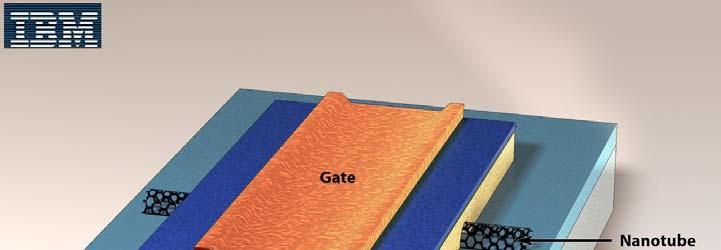
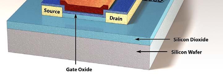
29 The carbon nanotubes

30 The magnetic nanocolumns Today Contribution of nanotechnologies granulary film in-plane magnetization 100 grains/bit nanometric columns perpendicular magnetization 1 bit per column


31 Molecular electronics A memory example Difficulty of realization J. SÉE - VSOP Lecture on Coulomb blockade for nanoelectronics
Lecture 16. Complementary metal oxide semiconductor (CMOS) CMOS 1-1
 CMOS 1-1") Lecture 16 Complementary metal oxide semiconductor (CMOS) CMOS 1-1 Outline Complementary metal oxide semiconductor (CMOS) Inverting circuit Properties Operating points Propagation delay Power dissipation
Lecture 16 Complementary metal oxide semiconductor (CMOS) CMOS 1-1 Outline Complementary metal oxide semiconductor (CMOS) Inverting circuit Properties Operating points Propagation delay Power dissipation
Field-Effect Transistor (FET) is one of the two major transistors; FET derives its name from its working mechanism;
 is one of the two major transistors; FET derives its name from its working mechanism;") Chapter 3 Field-Effect Transistors (FETs) 3.1 Introduction Field-Effect Transistor (FET) is one of the two major transistors; FET derives its name from its working mechanism; The concept has been known
Chapter 3 Field-Effect Transistors (FETs) 3.1 Introduction Field-Effect Transistor (FET) is one of the two major transistors; FET derives its name from its working mechanism; The concept has been known
EE105 Fall 2015 Microelectronic Devices and Circuits: MOSFET Prof. Ming C. Wu 511 Sutardja Dai Hall (SDH)
") EE105 Fall 2015 Microelectronic Devices and Circuits: MOSFET Prof. Ming C. Wu wu@eecs.berkeley.edu 511 Sutardja Dai Hall (SDH) 7-1 Simplest Model of MOSFET (from EE16B) 7-2 CMOS Inverter 7-3 CMOS NAND
EE105 Fall 2015 Microelectronic Devices and Circuits: MOSFET Prof. Ming C. Wu wu@eecs.berkeley.edu 511 Sutardja Dai Hall (SDH) 7-1 Simplest Model of MOSFET (from EE16B) 7-2 CMOS Inverter 7-3 CMOS NAND
Metal Oxide Semiconductor Field-Effect Transistors (MOSFETs)
") Metal Oxide Semiconductor Field-Effect Transistors (MOSFETs) Device Structure N-Channel MOSFET Providing electrons Pulling electrons (makes current flow) + + + Apply positive voltage to gate: Drives away
Metal Oxide Semiconductor Field-Effect Transistors (MOSFETs) Device Structure N-Channel MOSFET Providing electrons Pulling electrons (makes current flow) + + + Apply positive voltage to gate: Drives away
Introduction to VLSI ASIC Design and Technology
 Introduction to VLSI ASIC Design and Technology Paulo Moreira CERN - Geneva, Switzerland Paulo Moreira Introduction 1 Outline Introduction Is there a limit? Transistors CMOS building blocks Parasitics
Depletion-mode operation ( 공핍형 ): Using an input gate voltage to effectively decrease the channel size of an FET
: Using an input gate voltage to effectively decrease the channel size of an FET") Ch. 13 MOSFET Metal-Oxide-Semiconductor Field-Effect Transistor : I D D-mode E-mode V g The gate oxide is made of dielectric SiO 2 with e = 3.9 Depletion-mode operation ( 공핍형 ): Using an input gate voltage
Ch. 13 MOSFET Metal-Oxide-Semiconductor Field-Effect Transistor : I D D-mode E-mode V g The gate oxide is made of dielectric SiO 2 with e = 3.9 Depletion-mode operation ( 공핍형 ): Using an input gate voltage
MOSFET & IC Basics - GATE Problems (Part - I)
") MOSFET & IC Basics - GATE Problems (Part - I) 1. Channel current is reduced on application of a more positive voltage to the GATE of the depletion mode n channel MOSFET. (True/False) [GATE 1994: 1 Mark]
MOSFET & IC Basics - GATE Problems (Part - I) 1. Channel current is reduced on application of a more positive voltage to the GATE of the depletion mode n channel MOSFET. (True/False) [GATE 1994: 1 Mark]
Design cycle for MEMS
 Design cycle for MEMS Design cycle for ICs IC Process Selection nmos CMOS BiCMOS ECL for logic for I/O and driver circuit for critical high speed parts of the system The Real Estate of a Wafer MOS Transistor
Session 10: Solid State Physics MOSFET
 Session 10: Solid State Physics MOSFET 1 Outline A B C D E F G H I J 2 MOSCap MOSFET Metal-Oxide-Semiconductor Field-Effect Transistor: Al (metal) SiO2 (oxide) High k ~0.1 ~5 A SiO2 A n+ n+ p-type Si (bulk)
Microelectronics Circuit Analysis and Design
 Microelectronics Circuit Analysis and Design Donald A. Neamen Chapter 3 The Field Effect Transistor Neamen Microelectronics, 4e Chapter 3-1 In this chapter, we will: Study and understand the operation
Microelectronics Circuit Analysis and Design. MOS Capacitor Under Bias: Electric Field and Charge. Basic Structure of MOS Capacitor 9/25/2013
 Microelectronics Circuit Analysis and Design Donald A. Neamen Chapter 3 The Field Effect Transistor In this chapter, we will: Study and understand the operation and characteristics of the various types
ECE 340 Lecture 40 : MOSFET I
 ECE 340 Lecture 40 : MOSFET I Class Outline: MOS Capacitance-Voltage Analysis MOSFET - Output Characteristics MOSFET - Transfer Characteristics Things you should know when you leave Key Questions How do
ECE 340 Lecture 37 : Metal- Insulator-Semiconductor FET Class Outline:
 ECE 340 Lecture 37 : Metal- Insulator-Semiconductor FET Class Outline: Metal-Semiconductor Junctions MOSFET Basic Operation MOS Capacitor Things you should know when you leave Key Questions What is the
MOSFET Terminals. The voltage applied to the GATE terminal determines whether current can flow between the SOURCE & DRAIN terminals.
 MOSFET Terminals The voltage applied to the GATE terminal determines whether current can flow between the SOURCE & DRAIN terminals. For an n-channel MOSFET, the SOURCE is biased at a lower potential (often
Improved Inverter: Current-Source Pull-Up. MOS Inverter with Current-Source Pull-Up. What else could be connected between the drain and V DD?
 Improved Inverter: Current-Source Pull-Up MOS Inverter with Current-Source Pull-Up What else could be connected between the drain and? Replace resistor with current source I SUP roc i D v IN v OUT Find
Field Effect Transistors (FET s) University of Connecticut 136
 University of Connecticut 136") Field Effect Transistors (FET s) University of Connecticut 136 Field Effect Transistors (FET s) FET s are classified three ways: by conduction type n-channel - conduction by electrons p-channel - conduction
Field Effect Transistors (FET s) University of Connecticut 136 Field Effect Transistors (FET s) FET s are classified three ways: by conduction type n-channel - conduction by electrons p-channel - conduction
ECE 5745 Complex Digital ASIC Design Topic 2: CMOS Devices
 ECE 5745 Complex Digital ASIC Design Topic 2: CMOS Devices Christopher Batten School of Electrical and Computer Engineering Cornell University http://www.csl.cornell.edu/courses/ece5950 Simple Transistor
EE 330 Laboratory 7 MOSFET Device Experimental Characterization and Basic Applications Spring 2017
 EE 330 Laboratory 7 MOSFET Device Experimental Characterization and Basic Applications Spring 2017 Objective: The objective of this laboratory experiment is to become more familiar with the operation of
Lecture Integrated circuits era
 Lecture 1 1.1 Integrated circuits era Transistor was first invented by William.B.Shockley, Walter Brattain and John Bardeen of Bell laboratories. In 1961, first IC was introduced. Levels of Integration:-
Integrated Circuit Amplifiers. Comparison of MOSFETs and BJTs
 Integrated Circuit Amplifiers Comparison of MOSFETs and BJTs 17 Typical CMOS Device Parameters 0.8 µm 0.25 µm 0.13 µm Parameter NMOS PMOS NMOS PMOS NMOS PMOS t ox (nm) 15 15 6 6 2.7 2.7 C ox (ff/µm 2 )
Microelectronics, BSc course
 Microelectronics, BSc course MOS circuits: CMOS circuits, construction http://www.eet.bme.hu/~poppe/miel/en/14-cmos.pptx http://www.eet.bme.hu The abstraction level of our study: SYSTEM + MODULE GATE CIRCUIT
Field Effect Transistors
 Field Effect Transistors LECTURE NO. - 41 Field Effect Transistors www.mycsvtunotes.in JFET MOSFET CMOS Field Effect transistors - FETs First, why are we using still another transistor? BJTs had a small
Lecture 16: MOS Transistor models: Linear models, SPICE models. Context. In the last lecture, we discussed the MOS transistor, and
 Lecture 16: MOS Transistor models: Linear models, SPICE models Context In the last lecture, we discussed the MOS transistor, and added a correction due to the changing depletion region, called the body
Lecture 11 Digital Circuits (I) THE INVERTER
 THE INVERTER") Lecture 11 Digital Circuits (I) THE INVERTER Outline Introduction to digital circuits The inverter NMOS inverter with resistor pull-up Reading Assignment: Howe and Sodini; Chapter 5, Sections 5.1-5.3 6.12
Lecture 11 Digital Circuits (I) THE INVERTER Outline Introduction to digital circuits The inverter NMOS inverter with resistor pull-up Reading Assignment: Howe and Sodini; Chapter 5, Sections 5.1-5.3 6.12
Lecture #29. Moore s Law
 Lecture #29 ANNOUNCEMENTS HW#15 will be for extra credit Quiz #6 (Thursday 5/8) will include MOSFET C-V No late Projects will be accepted after Thursday 5/8 The last Coffee Hour will be held this Thursday
ECE380 Digital Logic. Logic values as voltage levels
 ECE380 Digital Logic Implementation Technology: NMOS and PMOS Transistors, CMOS logic gates Dr. D. J. Jackson Lecture 13-1 Logic values as voltage levels V ss is the minimum voltage that can exist in the
6.012 Microelectronic Devices and Circuits
 Page 1 of 13 YOUR NAME Department of Electrical Engineering and Computer Science Massachusetts Institute of Technology 6.012 Microelectronic Devices and Circuits Final Eam Closed Book: Formula sheet provided;
DIGITAL VLSI LAB ASSIGNMENT 1
 DIGITAL VLSI LAB ASSIGNMENT 1 Problem 1: NMOS and PMOS plots using Cadence. In this exercise, you are required to generate both NMOS and PMOS I-V device characteristics (I/P and O/P) using Cadence (Use
Lecture 13 - Digital Circuits (II) MOS Inverter Circuits. October 25, 2005
 MOS Inverter Circuits. October 25, 2005") 6.12 - Microelectronic Devices and Circuits - Fall 25 Lecture 13-1 Lecture 13 - Digital Circuits (II) MOS Inverter Circuits October 25, 25 Contents: 1. NMOS inverter with resistor pull-up (cont.) 2. NMOS
6.12 - Microelectronic Devices and Circuits - Fall 25 Lecture 13-1 Lecture 13 - Digital Circuits (II) MOS Inverter Circuits October 25, 25 Contents: 1. NMOS inverter with resistor pull-up (cont.) 2. NMOS
ECE/CoE 0132: FETs and Gates
 ECE/CoE 0132: FETs and Gates Kartik Mohanram September 6, 2017 1 Physical properties of gates Over the next 2 lectures, we will discuss some of the physical characteristics of integrated circuits. We will
Introduction to MOSFET MOSFET (Metal Oxide Semiconductor Field Effect Transistor)
") Microelectronic Circuits Introduction to MOSFET MOSFET (Metal Oxide Semiconductor Field Effect Transistor) Slide 1 MOSFET Construction MOSFET (Metal Oxide Semiconductor Field Effect Transistor) Slide 2
Microelectronic Circuits Introduction to MOSFET MOSFET (Metal Oxide Semiconductor Field Effect Transistor) Slide 1 MOSFET Construction MOSFET (Metal Oxide Semiconductor Field Effect Transistor) Slide 2
Lecture 11 Circuits numériques (I) L'inverseur
 L'inverseur") Lecture 11 Circuits numériques (I) L'inverseur Outline Introduction to digital circuits The inverter NMOS inverter with resistor pull-up 6.12 Spring 24 Lecture 11 1 1. Introduction to digital circuits:
Lecture 11 Circuits numériques (I) L'inverseur Outline Introduction to digital circuits The inverter NMOS inverter with resistor pull-up 6.12 Spring 24 Lecture 11 1 1. Introduction to digital circuits:
Transistor was first invented by William.B.Shockley, Walter Brattain and John Bardeen of Bell Labratories. In 1961, first IC was introduced.
 Unit 1 Basic MOS Technology Transistor was first invented by William.B.Shockley, Walter Brattain and John Bardeen of Bell Labratories. In 1961, first IC was introduced. Levels of Integration:- i) SSI:-
Lecture 4. MOS transistor theory
 Lecture 4 MOS transistor theory 1.7 Introduction: A MOS transistor is a majority-carrier device, in which the current in a conducting channel between the source and the drain is modulated by a voltage
Solid State Devices- Part- II. Module- IV
 Solid State Devices- Part- II Module- IV MOS Capacitor Two terminal MOS device MOS = Metal- Oxide- Semiconductor MOS capacitor - the heart of the MOSFET The MOS capacitor is used to induce charge at the
55:041 Electronic Circuits
 55:041 Electronic Circuits Mosfet Review Sections of Chapter 3 &4 A. Kruger Mosfet Review, Page-1 Basic Structure of MOS Capacitor Sect. 3.1 Width 1 10-6 m or less Thickness 50 10-9 m or less ` MOS Metal-Oxide-Semiconductor
Experiment 3. 3 MOSFET Drain Current Modeling. 3.1 Summary. 3.2 Theory. ELEC 3908 Experiment 3 Student#:
 Experiment 3 3 MOSFET Drain Current Modeling 3.1 Summary In this experiment I D vs. V DS and I D vs. V GS characteristics are measured for a silicon MOSFET, and are used to determine the parameters necessary
Organic Electronics. Information: Information: 0331a/ 0442/
 Organic Electronics (Course Number 300442 ) Spring 2006 Organic Field Effect Transistors Instructor: Dr. Dietmar Knipp Information: Information: http://www.faculty.iubremen.de/course/c30 http://www.faculty.iubremen.de/course/c30
Shorthand Notation for NMOS and PMOS Transistors
 Shorthand Notation for NMOS and PMOS Transistors Terminal Voltages Mode of operation depends on V g, V d, V s V gs = V g V s V gd = V g V d V ds = V d V s = V gs - V gd Source and drain are symmetric diffusion
problem grade total
 Fall 2005 6.012 Microelectronic Devices and Circuits Prof. J. A. del Alamo Name: Recitation: November 16, 2005 Quiz #2 problem grade 1 2 3 4 total General guidelines (please read carefully before starting):
8. Characteristics of Field Effect Transistor (MOSFET)
") 1 8. Characteristics of Field Effect Transistor (MOSFET) 8.1. Objectives The purpose of this experiment is to measure input and output characteristics of n-channel and p- channel field effect transistors
1 8. Characteristics of Field Effect Transistor (MOSFET) 8.1. Objectives The purpose of this experiment is to measure input and output characteristics of n-channel and p- channel field effect transistors
Chapter 2 : Semiconductor Materials & Devices (II) Feb
 Feb") Chapter 2 : Semiconductor Materials & Devices (II) 1 Reference 1. SemiconductorManufacturing Technology: Michael Quirk and Julian Serda (2001) 3. Microelectronic Circuits (5/e): Sedra & Smith (2004) 4.
Chapter 2 : Semiconductor Materials & Devices (II) 1 Reference 1. SemiconductorManufacturing Technology: Michael Quirk and Julian Serda (2001) 3. Microelectronic Circuits (5/e): Sedra & Smith (2004) 4.
Lecture-45. MOS Field-Effect-Transistors Threshold voltage
 Lecture-45 MOS Field-Effect-Transistors 7.4. Threshold voltage In this section we summarize the calculation of the threshold voltage and discuss the dependence of the threshold voltage on the bias applied
Basic Fabrication Steps
 Basic Fabrication Steps and Layout Somayyeh Koohi Department of Computer Engineering Adapted with modifications from lecture notes prepared by author Outline Fabrication steps Transistor structures Transistor
Department of Electrical Engineering IIT Madras
 Department of Electrical Engineering IIT Madras Sample Questions on Semiconductor Devices EE3 applicants who are interested to pursue their research in microelectronics devices area (fabrication and/or
Device Technologies. Yau - 1
 Device Technologies Yau - 1 Objectives After studying the material in this chapter, you will be able to: 1. Identify differences between analog and digital devices and passive and active components. Explain
NAME: Last First Signature
 UNIVERSITY OF CALIFORNIA, BERKELEY College of Engineering Department of Electrical Engineering and Computer Sciences EE 130: IC Devices Spring 2003 FINAL EXAMINATION NAME: Last First Signature STUDENT
Field Effect Transistors
 Chapter 5: Field Effect Transistors Slide 1 FET FET s (Field Effect Transistors) are much like BJT s (Bipolar Junction Transistors). Similarities: Amplifiers Switching devices Impedance matching circuits
Solid State Device Fundamentals
 Solid State Device Fundamentals 4.4. Field Effect Transistor (MOSFET) ENS 463 Lecture Course by Alexander M. Zaitsev alexander.zaitsev@csi.cuny.edu Tel: 718 982 2812 4N101b 1 Field-effect transistor (FET)
ENEE 307 Laboratory#2 (n-mosfet, p-mosfet, and a single n-mosfet amplifier in the common source configuration)
") Revised 2/16/2007 ENEE 307 Laboratory#2 (n-mosfet, p-mosfet, and a single n-mosfet amplifier in the common source configuration) *NOTE: The text mentioned below refers to the Sedra/Smith, 5th edition.
Revised 2/16/2007 ENEE 307 Laboratory#2 (n-mosfet, p-mosfet, and a single n-mosfet amplifier in the common source configuration) *NOTE: The text mentioned below refers to the Sedra/Smith, 5th edition.
EE 42/100 Lecture 23: CMOS Transistors and Logic Gates. Rev A 4/15/2012 (10:39 AM) Prof. Ali M. Niknejad
 Prof. Ali M. Niknejad") A. M. Niknejad University of California, Berkeley EE 100 / 42 Lecture 23 p. 1/16 EE 42/100 Lecture 23: CMOS Transistors and Logic Gates ELECTRONICS Rev A 4/15/2012 (10:39 AM) Prof. Ali M. Niknejad University
A. M. Niknejad University of California, Berkeley EE 100 / 42 Lecture 23 p. 1/16 EE 42/100 Lecture 23: CMOS Transistors and Logic Gates ELECTRONICS Rev A 4/15/2012 (10:39 AM) Prof. Ali M. Niknejad University
Digital Electronics. Assign 1 and 0 to a range of voltage (or current), with a separation that minimizes a transition region. Positive Logic.
, with a separation that minimizes a transition region. Positive Logic.") Digital Electronics Assign 1 and 0 to a range of voltage (or current), with a separation that minimizes a transition region Positive Logic Logic 1 Negative Logic Logic 0 Voltage Transition Region Transition
Digital Electronics Assign 1 and 0 to a range of voltage (or current), with a separation that minimizes a transition region Positive Logic Logic 1 Negative Logic Logic 0 Voltage Transition Region Transition
INTERNATIONAL JOURNAL OF APPLIED ENGINEERING RESEARCH, DINDIGUL Volume 1, No 3, 2010
 Low Power CMOS Inverter design at different Technologies Vijay Kumar Sharma 1, Surender Soni 2 1 Department of Electronics & Communication, College of Engineering, Teerthanker Mahaveer University, Moradabad
Sub-Threshold Region Behavior of Long Channel MOSFET
 Sub-threshold Region - So far, we have discussed the MOSFET behavior in linear region and saturation region - Sub-threshold region is refer to region where Vt is less than Vt - Sub-threshold region reflects
INTRODUCTION: Basic operating principle of a MOSFET:
 INTRODUCTION: Along with the Junction Field Effect Transistor (JFET), there is another type of Field Effect Transistor available whose Gate input is electrically insulated from the main current carrying
BJT Amplifier. Superposition principle (linear amplifier)
") BJT Amplifier Two types analysis DC analysis Applied DC voltage source AC analysis Time varying signal source Superposition principle (linear amplifier) The response of a linear amplifier circuit excited
BJT Amplifier Two types analysis DC analysis Applied DC voltage source AC analysis Time varying signal source Superposition principle (linear amplifier) The response of a linear amplifier circuit excited
Q1. Explain the construction and principle of operation of N-Channel and P-Channel Junction Field Effect Transistor (JFET).
.") Q. Explain the construction and principle of operation of N-Channel and P-Channel Junction Field Effect Transistor (JFET). Answer: N-Channel Junction Field Effect Transistor (JFET) Construction: Drain(D)
Q. Explain the construction and principle of operation of N-Channel and P-Channel Junction Field Effect Transistor (JFET). Answer: N-Channel Junction Field Effect Transistor (JFET) Construction: Drain(D)
ECE520 VLSI Design. Lecture 2: Basic MOS Physics. Payman Zarkesh-Ha
 ECE520 VLSI Design Lecture 2: Basic MOS Physics Payman Zarkesh-Ha Office: ECE Bldg. 230B Office hours: Wednesday 2:00-3:00PM or by appointment E-mail: pzarkesh@unm.edu Slide: 1 Review of Last Lecture Semiconductor
Fin-Shaped Field Effect Transistor (FinFET) Min Ku Kim 03/07/2018
 Min Ku Kim 03/07/2018") Fin-Shaped Field Effect Transistor (FinFET) Min Ku Kim 03/07/2018 ECE 658 Sp 2018 Semiconductor Materials and Device Characterizations OUTLINE Background FinFET Future Roadmap Keeping up w/ Moore s Law
Fin-Shaped Field Effect Transistor (FinFET) Min Ku Kim 03/07/2018 ECE 658 Sp 2018 Semiconductor Materials and Device Characterizations OUTLINE Background FinFET Future Roadmap Keeping up w/ Moore s Law
Laboratory #5 BJT Basics and MOSFET Basics
 Laboratory #5 BJT Basics and MOSFET Basics I. Objectives 1. Understand the physical structure of BJTs and MOSFETs. 2. Learn to measure I-V characteristics of BJTs and MOSFETs. II. Components and Instruments
Lecture 31 - The Short Metal-Oxide-Semiconductor Field-Effect Transistor (cont.) April 25, 2007
 April 25, 2007") 6.720J/3.43J - Integrated Microelectronic Devices - Spring 2007 Lecture 31-1 Lecture 31 - The Short Metal-Oxide-Semiconductor Field-Effect Transistor (cont.) April 25, 2007 Contents: 1. Short-channel effects
6.720J/3.43J - Integrated Microelectronic Devices - Spring 2007 Lecture 31-1 Lecture 31 - The Short Metal-Oxide-Semiconductor Field-Effect Transistor (cont.) April 25, 2007 Contents: 1. Short-channel effects
MOS TRANSISTOR THEORY
 MOS TRANSISTOR THEORY Introduction A MOS transistor is a majority-carrier device, in which the current in a conducting channel between the source and the drain is modulated by a voltage applied to the
ECEN325: Electronics Summer 2018
 ECEN325: Electronics Summer 2018 Metal-Oxide-Semiconductor Field Effect Transistor (MOSFET) Sam Palermo Analog & Mixed-Signal Center Texas A&M University Announcements & Reading H5 due today Exam 2 on
3.CMOS Inverter-homework
 3.CMOS Inverter-homework 1. for a CMOS inverter, when the pmos and nmos are long-channel devices,or when the supply voltage is low, velocity does not occur, under these circumstances,vm(vin=vout)=? 2.
EXPERIMENT # 1: REVERSE ENGINEERING OF INTEGRATED CIRCUITS Week of 1/17/05
 EXPERIMENT # 1: REVERSE ENGINEERING OF INTEGRATED CIRCUITS Week of 1/17/5 Experiment #1: Reading: Reverse engineering of integrated circuits Jaeger 9.2: MOS transistor layout and design rules HP4145 basics:
Introduction to the Long Channel MOSFET. Dr. Lynn Fuller
 ROCHESTER INSTITUTE OF TECHNOLOGY MICROELECTRONIC ENGINEERING Introduction to the Long Channel MOSFET Dr. Lynn Fuller Webpage: http://people.rit.edu/lffeee Electrical and 82 Lomb Memorial Drive Rochester,
Power and Energy. Courtesy of Dr. Daehyun Dr. Dr. Shmuel and Dr.
 Power and Energy Courtesy of Dr. Daehyun Lim@WSU, Dr. Harris@HMC, Dr. Shmuel Wimer@BIU and Dr. Choi@PSU http://csce.uark.edu +1 (479) 575-6043 yrpeng@uark.edu The Chip is HOT Power consumption increases
ECE 546 Lecture 12 Integrated Circuits
 ECE 546 Lecture 12 Integrated Circuits Spring 2018 Jose E. Schutt-Aine Electrical & Computer Engineering University of Illinois jesa@illinois.edu ECE 546 Jose Schutt Aine 1 Integrated Circuits IC Requirements
Chapter 5: Field Effect Transistors
 Chapter 5: Field Effect Transistors Slide 1 FET FET s (Field Effect Transistors) are much like BJT s (Bipolar Junction Transistors). Similarities: Amplifiers Switching devices Impedance matching circuits
UNIT-1 Bipolar Junction Transistors. Text Book:, Microelectronic Circuits 6 ed., by Sedra and Smith, Oxford Press
 UNIT-1 Bipolar Junction Transistors Text Book:, Microelectronic Circuits 6 ed., by Sedra and Smith, Oxford Press Figure 6.1 A simplified structure of the npn transistor. Microelectronic Circuits, Sixth
Metal-Oxide-Silicon (MOS) devices PMOS. n-type
 devices PMOS. n-type") Metal-Oxide-Silicon (MOS devices Principle of MOS Field Effect Transistor transistor operation Metal (poly gate on oxide between source and drain Source and drain implants of opposite type to substrate.
Metal-Oxide-Silicon (MOS devices Principle of MOS Field Effect Transistor transistor operation Metal (poly gate on oxide between source and drain Source and drain implants of opposite type to substrate.
Lecture 12 - Digital Circuits (I) The inverter. October 20, 2005
 The inverter. October 20, 2005") 6.12 - Microelectronic Devices and Circuits - Fall 25 Lecture 12-1 Lecture 12 - Digital Circuits (I) The inverter October 2, 25 Contents: 1. Introduction to digital electronics: the inverter 2. NMOS inverter
6.12 - Microelectronic Devices and Circuits - Fall 25 Lecture 12-1 Lecture 12 - Digital Circuits (I) The inverter October 2, 25 Contents: 1. Introduction to digital electronics: the inverter 2. NMOS inverter
LECTURE 09 LARGE SIGNAL MOSFET MODEL
 Lecture 9 Large Signal MOSFET Model (5/14/18) Page 9-1 LECTURE 9 LARGE SIGNAL MOSFET MODEL LECTURE ORGANIZATION Outline Introduction to modeling Operation of the MOS transistor Simple large signal model
Design and Simulation of Low Voltage Operational Amplifier
 Design and Simulation of Low Voltage Operational Amplifier Zach Nelson Department of Electrical Engineering, University of Nevada, Las Vegas 4505 S Maryland Pkwy, Las Vegas, NV 89154 United States of America
University of Pittsburgh
 University of Pittsburgh Experiment #4 Lab Report MOSFET Amplifiers and Current Mirrors Submission Date: 07/03/2018 Instructors: Dr. Ahmed Dallal Shangqian Gao Submitted By: Nick Haver & Alex Williams
ENG2410 Digital Design CMOS Technology. Fall 2017 S. Areibi School of Engineering University of Guelph
 ENG2410 Digital Design CMOS Technology Fall 2017 S. reibi School of Engineering University of Guelph The Transistor Revolution First transistor Bell Labs, 1948 Bipolar logic 1960 s Intel 4004 processor
Topic 3. CMOS Fabrication Process
 Topic 3 CMOS Fabrication Process Peter Cheung Department of Electrical & Electronic Engineering Imperial College London URL: www.ee.ic.ac.uk/pcheung/ E-mail: p.cheung@ic.ac.uk Lecture 3-1 Layout of a Inverter
Lecture 33 - The Short Metal-Oxide-Semiconductor Field-Effect Transistor (cont.) April 30, 2007
 April 30, 2007") 6.720J/3.43J - Integrated Microelectronic Devices - Spring 2007 Lecture 33-1 Lecture 33 - The Short Metal-Oxide-Semiconductor Field-Effect Transistor (cont.) April 30, 2007 Contents: 1. MOSFET scaling
6.720J/3.43J - Integrated Microelectronic Devices - Spring 2007 Lecture 33-1 Lecture 33 - The Short Metal-Oxide-Semiconductor Field-Effect Transistor (cont.) April 30, 2007 Contents: 1. MOSFET scaling
Week 9a OUTLINE. MOSFET I D vs. V GS characteristic Circuit models for the MOSFET. Reading. resistive switch model small-signal model
 Week 9a OUTLINE MOSFET I vs. V GS characteristic Circuit models for the MOSFET resistive switch model small-signal model Reading Rabaey et al.: Chapter 3.3.2 Hambley: Chapter 12 (through 12.5); Section
MEASUREMENT AND INSTRUMENTATION STUDY NOTES UNIT-I
 MEASUREMENT AND INSTRUMENTATION STUDY NOTES The MOSFET The MOSFET Metal Oxide FET UNIT-I As well as the Junction Field Effect Transistor (JFET), there is another type of Field Effect Transistor available
55:041 Electronic Circuits
 55:041 Electronic Circuits MOSFETs Sections of Chapter 3 &4 A. Kruger MOSFETs, Page-1 Basic Structure of MOS Capacitor Sect. 3.1 Width = 1 10-6 m or less Thickness = 50 10-9 m or less ` MOS Metal-Oxide-Semiconductor
EEC 118 Spring 2010 Lab #1: NMOS and PMOS Transistor Parameters
 EEC 118 Spring 2010 Lab #1: NMOS and PMOS Transistor Parameters Dept. of Electrical and Computer Engineering University of California, Davis March 18, 2010 Reading: Rabaey Chapter 3 [1]. Reference: Kang
UNIVERSITY OF CALIFORNIA AT BERKELEY College of Engineering Department of Electrical Engineering and Computer Sciences.
 UNIVERSITY OF CALIFORNIA AT BERKELEY College of Engineering Department of Electrical Engineering and Computer Sciences Discussion #9 EE 05 Spring 2008 Prof. u MOSFETs The standard MOSFET structure is shown
Low Power Realization of Subthreshold Digital Logic Circuits using Body Bias Technique
 Indian Journal of Science and Technology, Vol 9(5), DOI: 1017485/ijst/2016/v9i5/87178, Februaru 2016 ISSN (Print) : 0974-6846 ISSN (Online) : 0974-5645 Low Power Realization of Subthreshold Digital Logic
MOS Field Effect Transistors
 MOS Field Effect Transistors A gate contact gate interconnect n polysilicon gate source contacts W active area (thin oxide area) polysilicon gate contact metal interconnect drain contacts A bulk contact
The CMOS Inverter. Lecture 3a Static properties (VTC and noise margins)
") The CMOS Inverter Lecture 3a Static properties (VTC and noise margins) Why so much about inverters? The current that any CMOS logic gate can deliver or sink can be calculated from equivalent inverter!
The CMOS Inverter Lecture 3a Static properties (VTC and noise margins) Why so much about inverters? The current that any CMOS logic gate can deliver or sink can be calculated from equivalent inverter!
Lecture 26 - Design Problems & Wrap-Up. May 15, 2003
 6.012 Microelectronic Devices and Circuits - Spring 2003 Lecture 26-1 Lecture 26 - Design Problems & 6.012 Wrap-Up May 15, 2003 Contents: 1. Design process 2. Design project pitfalls 3. Lessons learned
3-D Modelling of the Novel Nanoscale Screen-Grid Field Effect Transistor (SGFET)
") 3-D Modelling of the Novel Nanoscale Screen-Grid Field Effect Transistor (SGFET) Pei W. Ding, Kristel Fobelets Department of Electrical Engineering, Imperial College London, U.K. J. E. Velazquez-Perez
3-D Modelling of the Novel Nanoscale Screen-Grid Field Effect Transistor (SGFET) Pei W. Ding, Kristel Fobelets Department of Electrical Engineering, Imperial College London, U.K. J. E. Velazquez-Perez
MOS Transistor Theory
 MOS Transistor Theory So far, we have viewed a MOS transistor as an ideal switch (digital operation) Reality: less than ideal EE 261 Krish Chakrabarty 1 MOS Transistor Theory Study conducting channel between
EE 230 Lab Lab 9. Prior to Lab
 MOS transistor characteristics This week we look at some MOS transistor characteristics and circuits. Most of the measurements will be done with our usual lab equipment, but we will also use the parameter
Atomic-layer deposition of ultrathin gate dielectrics and Si new functional devices
 Atomic-layer deposition of ultrathin gate dielectrics and Si new functional devices Anri Nakajima Research Center for Nanodevices and Systems, Hiroshima University 1-4-2 Kagamiyama, Higashi-Hiroshima,
MODELLING AND IMPLEMENTATION OF SUBTHRESHOLD CURRENTS IN SCHOTTKY BARRIER CNTFETs FOR DIGITAL APPLICATIONS
 www.arpapress.com/volumes/vol11issue3/ijrras_11_3_03.pdf MODELLING AND IMPLEMENTATION OF SUBTHRESHOLD CURRENTS IN SCHOTTKY BARRIER CNTFETs FOR DIGITAL APPLICATIONS Roberto Marani & Anna Gina Perri Electrical
MTLE-6120: Advanced Electronic Properties of Materials. Semiconductor transistors for logic and memory. Reading: Kasap
 MTLE-6120: Advanced Electronic Properties of Materials 1 Semiconductor transistors for logic and memory Reading: Kasap 6.6-6.8 Vacuum tube diodes 2 Thermionic emission from cathode Electrons collected
CHAPTER-2 BASICS. The Basics chapter emphasizes upon the various concepts that are
 8 CHAPTER-2 BASICS The Basics chapter emphasizes upon the various concepts that are involved in the functioning of MOS devices, effect of threshold voltage on characteristics, sub threshold conduction,
Three Terminal Devices
 Three Terminal Devices - field effect transistor (FET) - bipolar junction transistor (BJT) - foundation on which modern electronics is built - active devices - devices described completely by considering
The Design and Realization of Basic nmos Digital Devices
 Proceedings of The National Conference On Undergraduate Research (NCUR) 2004 Indiana University Purdue University Indianapolis, Indiana April 15-17, 2004 The Design and Realization of Basic nmos Digital
Future MOSFET Devices using high-k (TiO 2 ) dielectric
 dielectric") Future MOSFET Devices using high-k (TiO 2 ) dielectric Prerna Guru Jambheshwar University, G.J.U.S. & T., Hisar, Haryana, India, prernaa.29@gmail.com Abstract: In this paper, an 80nm NMOS with high-k (TiO
Future MOSFET Devices using high-k (TiO 2 ) dielectric Prerna Guru Jambheshwar University, G.J.U.S. & T., Hisar, Haryana, India, prernaa.29@gmail.com Abstract: In this paper, an 80nm NMOS with high-k (TiO
UNIT 3: FIELD EFFECT TRANSISTORS
 FIELD EFFECT TRANSISTOR: UNIT 3: FIELD EFFECT TRANSISTORS The field effect transistor is a semiconductor device, which depends for its operation on the control of current by an electric field. There are
Lecture Wrap up. December 13, 2005
 6.012 Microelectronic Devices and Circuits Fall 2005 Lecture 26 1 Lecture 26 6.012 Wrap up December 13, 2005 Contents: 1. 6.012 wrap up Announcements: Final exam TA review session: December 16, 7:30 9:30
EE241 - Spring 2013 Advanced Digital Integrated Circuits. Announcements. Sign up for Piazza if you haven t already
 EE241 - Spring 2013 Advanced Digital Integrated Circuits Lecture 2: Scaling Trends and Features of Modern Technologies Announcements Sign up for Piazza if you haven t already 2 1 Assigned Reading R.H.