MP103 EasyPower TM. Higher Power Offline Inductor-Less Regulator For Low Power Applications DESCRIPTION FEATURES APPLICATIONS TYPICAL APPLICATION
|
|
|
- Earl Kelley
- 5 years ago
- Views:
Transcription
1 The Fuure of Analog IC Technology MP13 EasyPower TM Higher Power Offline Inducor-Less Regulaor For Low Power Applicaions DESCRIPTION The MP13 provides an easy and low cos ACDC soluion for less han 1W applicaions. I is an off-line linear regulaor ha delivers good efficiency while generaing lile EMI noise. I provides an easy soluion o sep down he AC line volage o a regulaed DC volage. This offline linear regulaor replaces he convenional swiching regulaor, no needing a ransformer or an inducor. Due o is simpliciy, i offers an overall low BOM cos. MP13 delivers nearly wo imes he oupu power han he MP1 or MP1L by charging is capacior wih an exernal bipolar ransisor. MP13 maximizes efficiency by minimizing he volage drop beween and VOUT, while only charging when VIN is less han approximaely 32V. The MP13 enables he overall sysem o mee sandby power requiremens. MP13 offers rich proecions, such as Thermal Shudown (TSD), Over Temperaure Proecion (OTP), Over Volage Proecion (OVP), Shor o GND Proecion, Over Load Proecion (OLP), Shor Circui Proecion (SCP), MP13 is available in he SOIC8E package. FEATURES Universal AC Inpu (85Vac-35Vac) Inducor-less Less han 1mW sandby power Excellen EMI Performance Lower BOM Cos Smar Conrol o Maximizes Efficiency Adjusable Oupu Volage from 1.5V o 15V Good Line and Load Regulaion Drives Exernal BJT Shor Circui Proecion Exernal Programmable Over Temperaure Proecion (OTP) APPLICATIONS Wall swiches and dimmers AC/DC Power Supply for Wireless Sysem, like ZigBee, Z-Wave Sandby Power for General Off-Line Applicaions All MPS pars are lead-free and adhere o he RoHS direcive. For MPS green saus, please visi MPS websie under Producs, Qualiy Assurance page. MPS and The Fuure of Analog IC Technology are regisered rademarks of Monolihic Power Sysems, Inc. TPICAL APPLICATION MP13 Rev
2 ORDERING INFORMATION Par Number* Package Top Marking MP13GN SOIC8E MP13 * For Tape & Reel, add suffix Z (e.g. MP13GN Z); PACKAGE REFERENCE TOP VIEW RT 1 8 VIN GND 2 7 NC FB 3 6 DR VOUT 4 5 EXPOSED PAD ON BACK SIDE ABSOLUTE MAXIMUM RATINGS (1) VIN V o 7V VOUT V o 15V V o 35V DR V o 3V FB V o 6.5V RT -.3V o 6.5V Coninuous Power Dissipaion (T A = +25 C) (2) SOIC8E...2.5W Juncion Temperaure o C Lead Temperaure o C Sorage Temperaure o C o +15 o C ESD Capabiliy Human Body Mode 2kV Recommended Operaing Condiions (3) 5/6Hz AC RMS Volage... 85V o 35V... 8V o 3V Operaing Juncion Temp T J...-4 C o +15 C Thermal Resisance (4) θ JA θ JC SOIC8E C/W Noes: 1) Exceeding hese raings may damage he device. 2) The maximum allowable power dissipaion is a funcion of he maximum juncion emperaure T J (MAX), he juncion-oambien hermal resisance θ JA, and he ambien emperaure T A. The maximum allowable coninuous power dissipaion a any ambien emperaure is calculaed by P D (MAX) = (T J (MAX)-T A)/θ JA. Exceeding he maximum allowable power dissipaion will cause excessive die emperaure, and he regulaor will go ino hermal shudown. Inernal hermal shudown circuiry proecs he device from permanen damage. 3) The device is no guaraneed o funcion ouside of is operaing condiions. 4) Measured on JESD51-7, 4-layer PCB. MP13 Rev
3 ELECTRICAL CHARACTERISTICS T A = -4 C o +125 C, C FB =1pF, C OUT =2.2μF, C =4.7μF, unless oherwise noed. Parameer Symbol Condiion Min Typ Max Unis VIN Secion Inpu Volage VIN 65 V Inpu Supply Curren (Quiescen) IIN QC VIN= 9V & =V, No load μa Inpu Volage Slow Threshold VIN THS VIN Rising V Inpu Volage Slow Threshold Hyseresis VIN THS _ HS 3.2 V Inpu Volage Fas Threshold VIN THF VIN Rising V Inpu Volage Fas Threshold Hyseresis Secion VIN THF _ HS 5.7 V VOUT=5V V Peak Volage Limi PKLMT VOUT=12V V VOUT=5V 7 mv Peak Volage Hyseresis PKLMT _ HS VOUT=12V 83 mv Under Volage Lock Ou UVLO V Oupu Enable Threshold THOUT V Supply Curren (Quiescen) QC =3V ma Acive Bleeder ON BLDON VOUT=5V V VOUT=12V V VOUT=5V 6 mv Acive Bleeder ON Hyseresis BLDON _ HS VOUT=12V 7 mv Acive Bleeder Curren DR Secion IB BLD T A = -4 o C o 25 o C μa T A = 25 o C o 85 o C 53 μa T A = 85 o C o 125 o C μa Driver Curren IDR > THOUT ma Sarup Driver Curren IDR STARTUP < THOUT ma Base Curren Rise Rae (5) IDR RISERATE 2.7 ma/μs Base Curren Fall Rae (5) IDR FALLRATE 2.15 ma/μs VOUT Secion VOUT Regulaed Volage VOUT V Oupu Curren Capabiliy (6) IOUT VAC=3rms, β=1,idr=2ma 5 ma Oupu Curren Limi IOUT LMT =15V ma Line Regulaion (7) =13V o 3V, IOUT=1μA.4 % Load Regulaion (8) =3V, IOUT=1μA o 4mA.14 % MP13 Rev
4 ELECTRICAL CHARACTERISTICS (5) (coninued) T A = -4 C o +125 C, C FB =1pF, C OUT =2.2μF, C =4.7μF, unless oherwise noed. Parameer Symbol Condiion Min Typ Max Unis Dropou Volage (9) V DROP =2V,IOUT=4mA.55 V Ground Pin Curren I G =2V,IOUT=4mA 1.31 ma PSRR (1) PSRR 1~6kHz,CIN=1μF,COUT=4.7μF <6 db FB Secion Reference Volage VFB REF V RT Secion Oupu Curren of RT Pin IRT RI=1kΩ (11) μa RT Low Threshold Volage VRT THL V RT Threshold Volage Hyseresis VRT TH _ HS 6 mv RT Pin Open Volage VRT OPEN V Thermal Shudown Thermal Threshold Shudown T SD 16 ºC Thermal Shudown T Threshold Hyseresis SD _ HS 2 ºC Noes: 5) Took he linear region (Curren) measure Time1 a 2% and Time2 a 8% o calculae he base curren rise and fall rae. 6) Evaluae on E. 7) Line Regulaion = =3V, 1uA load - =13V, 1uA load) / 12V * 1. 8) Load Regulaion = =3V, 4mA load - =3V,1uA load) / 12V * 1. 9) The dropou volage is defined as -VOUT. 1) Guaranee by design. 11) Or force 5V and.5v on RT, hen measure RT curren. MP13 Rev
5 TPICAL CHARACTERISTICS MP13 Rev
6 TPICAL CHARACTERISTICS (coninued) LOAD CURRENT (ma) T k 5k 2k 6k MP13 Rev


7 TPICAL PERFORMANCE CHARACTERISTICS Performance waveforms are esed on he evaluaion board of he Design Example secion. V IN =23V AC, V OUT =5V, I OUT =6mA, C =47μF/25V, T A =+25 o C, unless oherwise noed. MP13 Rev


8 TPICAL PERFORMANCE CHARACTERISTICS (coninued) Performance waveforms are esed on he evaluaion board of he Design Example secion. V IN =23V AC, V OUT =5V, I OUT =6mA, C =47μF/25V, T A =+25 o C, unless oherwise noed. MP13 Rev
9 PIN FUNCTIONS Pin # Name Descripion 1 RT Temperaure sensing inpu pin. Conneced hrough a NTC resisor o GND. Once he volage of he RT pin drops below a fixed limi of.8v, DR oupu and LDO will be disabled. Le his pin floa if exernal emperaure sensing funcion is no used. 2 GND Ground. 3 FB Oupu volage feedback. Connec o a capacior o VOUT o improve low dropou sabiliy. Inernally volage divider se he oupu o be 12V. Connec o he ap of a resisor divider o adjus he oupu volage. 4 VOUT Oupu Volage. 5 Connec a cap from his pin o GND o sore he energy for he low drop-ou sage. 6 DR BJT driver pin.the driver is capable of providing.2a source curren o drive exernal BJT. 7 NC No conneced. 8 VIN Volage inpu supply. Providing energy when he volage falls wihin he charging window. Exposed Pad Connec o a large copper surface conneced o GND o enhance hermal dissipaion. MP13 Rev
10 BLOCK DIAGRAM RT OTP Faul VIN VOUT Acive Bleeder GND VOUT Adapive Charging Window Conrol NC FB BJT Driver DR Mode Selec Sarup/Seady Sae VOUT Volage Regulaor Figure 1: Funcional Block Diagram MP13 Rev
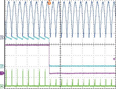
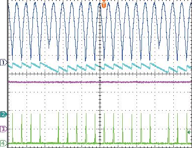
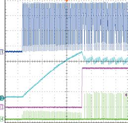
11 OPERATION MP13 employs a smar inducor-less regulaor design o supply a regulaed DC volage from an AC inpu. A unique (paen pending) charge algorihm ransfers charge from he AC line when he line volage is below 32V o he capacior (C1 in he ypical applicaion diagram). The capacior is used as he charge reservoir for an inernal LDO o regulae VOUT. There are wo disinc modes of normal operaion; sarup and seady sae. Sarup A sar up, all pins are a zero vols, and he AC line supplies power o VIN hrough he recifier. An inernal 19mA curren source is enabled beween VIN and DR. This curren drives he base of an exernal bipolar ransisor which charges he capacior. This inernal curren source is only enabled when VIN is wihin is charging window, ypically below 32V. This charging echnique minimizes power loss during sar up. During his sar up condiion, <15.25V, he oupu regulaor is disabled. As long as < 15.25V, DR provides 19mA during is charging window which limis he oupu curren if is shored. When >15.25V, he oupu regulaor is enabled, and MP13 eners is seady sae mode. IDR IDR STARTUP =19mA UVLO IDR=2mA THOUT Figure 2: Base Curren vs. Volage Seady sae In seady sae mode, DR curren is increased o 2mA. Figure 2 depics he relaionship of he DR/base curren o volage. I is enabled during is charging window of VIN< 32V. This echnique adapively replenishes he capacior charge which supplies power o he LDO. This enables good efficiency. An inernal comparaor will limi he volage. These are he peak hresholds lised in he elecrical able. This furher improves efficiency by opimally limiing he drop ou volage depending on VOUT. If falls below 7.6V, he regulaor will be disabled, urning off he power supply. The EMI performance is enhanced by urning on and off he curren source a a conrolled rae. The following secions describe in much more deail he seady sae operaion. Figure 3 depics he seady sae waveforms for beer undersanding. VIN IDR IIN v v2 VIN THS v3 4 5 Figure 3: Seady Sae Waveform [1, 2]: A he ime of 1, he volage of and VIN is equal, hen VIN is rising higher han, so here will be some charge curren flowing ino capacior; A he ime of 2, VIN reaches he slow urn-off hreshold, he inpu curren increased o is maximum value; [2, 3]: To benefi he EMI performance, MP13 will urn on and urn off he exernal BJT slowly wih cerain rae. A he ime of 2, he driver reduces he driver curren slowly o urn off he exernal BJT, a he ime of 3, he exernal BJT is oally urned off; [3, 4]: During his period, he VIN is higher han he slow urn-off hreshold, he driver is urned off and no curren flowing ino capacior, he capacior provides he power o LDO for oupu load, a he ime of 4, he volage of drops from v2 o v3; 6 v4 MP13 Rev
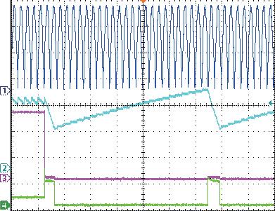
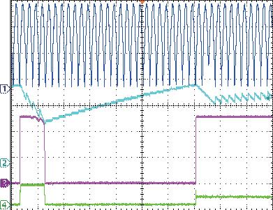
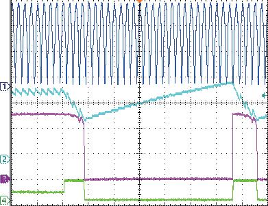
12 [4, 5]: A he ime of 4, VIN falls o he slow urn-on hreshold; he driver curren begins o slowly rise o urn on he exernal BJT, a he ime of 5, he exernal BJT is fully on; [5, 6]: As VIN falls, he charging curren is decreased, and he volage is increased by he charge curren. A he ime of 6, VIN falls o he value equal o volage, here is no curren flowing ino capacior; [6, 1]: During his period, alhough he driver is acive, since VIN is lower han volage, so here is no charging curren, he capacior provide he power for he oupu load and he volage drop from v4 o v1 a he ime of 1; Adapive Acive Charging Window To minimize he power loss of BJT and LDO, MP13 inegraes an adapive acive charging window conrol, which mainain he maximum volage difference beween and VOUT say a a consan level, hus he peak volage is limied relaed o VOUT. When VIN varies from high o low volage ino is charging window and he volage is lower han PKLMT minus PKLMT _HS, hen he driver will be urned on and capacior will be charged up. If volage is charged up o is peak limi PKLMT which is relaed wih he oupu volage, hen he driver will be slowly urned off alhough VIN doesn reach is slow urn-off hreshold. Figure 4 depics he siuaion ha reaches is peak limi when VIN is in is charging window. VIN VIN THS PKLMT PKLMT_HS Acive Bleeder Circui Due o he parasiic capacior of VIN o GND, he inpu volage may no fall ino is charging window during normal operaion. A sar up, he acive bleeder is always on o pull down he inpu volage ino is charging window o charge capacior o is oupu enable hreshold THOUT a which momen he LDO is enabled. During seady sae mode, o guaranee he oupu ge enough energy from inpu pors, acive bleeder circui is enabled whenever he volage falls below BLDON. Besides, when he power supply is shu down, acive bleeder circui discharges he energy sored in parasiic capacior o ensure he circui can resar easily. Shor Circui Proecion The oupu curren is limied o 17mA (IOUT LMT ) if he oupu is shored o ground, which also decreases he volage. When drops below 7.6V ( UVLO ), he LDO urns off. The inpu volage hen gradually charges up o 15.25V ( THOUT ) o enable he LDO. When LDO urns on, he oupu curren drops he volage o 7.6V again. This process will coninue unil he oupu shor condiion ceases. Over Load Proecion The and VOUT volages will drop simulaneously if he oupu curren exceeds is normal value. When he volage falls o 7.6V ( UVLO ), he second sage LDO shus down immediaely. Then he inpu volage charges o 15.25V ( THOUT ) o enable he LDO. Due o he oupu curren limi circui, he maximum curren is limied o 17mA (IOUT LMT ) ypically. Shor o GND Proecion When is shored o GND, he driver curren will be reduced o 19mA (IDR STARTUP ) ypically o decrease he power consumpion of exernal BJT, hus he hermal damage of exernal BJT is prevened. IDR IIN Figure 4: Adapive Acive Charging Window Over Temperaure Proecion An NTC resisor in series wih a regular resisor can be conneced beween RT and GND for MP13 Rev
13 ambien emperaure sensing and proecion. The value of he NTC resisor becomes lower when he ambien emperaure rises. Wih he fixed inernal curren 8uA flowing hrough he resisors, he volage of RT pin becomes lower a high emperaure. When VRT is lower han VRT THL ( ypically.8v ), hen inernal OTP circui will be riggered and he BJT driver and LDO will be shu down immediaely. When VRT is higher han VRT THL plus VRT TH _ HS, hen MP13 will resar. Thermal Shudown Proecion Accurae emperaure proecion prevens he chip from operaing a exceedingly high emperaures. When he silicon die emperaure exceeds 16 o C, he whole chip shus down. When he emperaure falls below is lower hreshold of 14 o C, he chip is enabled again. MP13 Rev
14 APPLICATION INFROMATION COMPONENT SELECTION Seing he Oupu Volage The oupu volage is se o 12V by inernal large feedback resisors. Typically, he inernal upper and lower feedback resisor is 1.125MΩ and 125kΩ respecively. Adjus VOUT by choosing appropriae exernal feedback resisors. The recommended oupu volage is beween 1.5V and 15V. Defining he upper and lower feedback resisors as R UP and R LW respecively (refer o he picure in Typical Applicaion secion): VOUT RUP = R LW ( 1) For he exernal resisors o dominae over he inernal resisors, selec relaively small values of R UP and R LW compared o he inernal resisors. However, o minimize he load consumpion, avoid very small exernal resisors. For mos applicaions, choose R LW =1.2kΩ. To accuraely se he oupu volage, selec R UP ha can couner he inernal upper-feedback resisor value of 1.125MΩ ypically. The able below liss ypical resisor values for differen oupu volages. Table 1: Resisors Selecing vs. Oupu Volage Seing VOUT (V) R UP (kω) R LW (kω) (1%) 1.2 (1%) (1%) 1.2 (1%) (1%) 1.2 (1%) (1%) 1.2 (1%) Selecion of Capacior The bypass capacior on he pin needs o be sufficienly large o suppor sufficien energy. Calculae he capaciance (in μf) based on he following equaion: I τ C = OUT s Vripple Where, I OUT is he oupu curren (ma); τ s is based on he ype of inpu recifier for example, τ is 2ms for a half-wave recifier, and 1ms for s a full-bridge recifier, V ripple is he volage ripple on he capacior normally he ripple is limied o 2V o 3V. For bes resuls, use a small ceramic capacior and a large aluminum capacior in parallel. Oupu Power Capabiliy The following facors influence he MP13 s maximum oupu power: he inpu recifier (full bridge or half-wave); he capacior conneced beween and GND; he DC curren gain and collecor curren of exernal BJT; he oupu volage and he emperaure-rise requiremen of key componens, which is relevan o differen applicaion environmens. V AC V IN GND Full Bridge Recifier V AC V IN GND Half-wave Recifier Figure 5 depics he relaionship beween he maximum oupu power and he VIN volage when he oupu volage is 12V, 5V and 3.3V respecively. The plos accoun for he full bridge recifiers, he emperaure rise of MP13 is less han 6 o C on he es board in 25 o C room emperaure es Figure 5: Oupu Power vs. Inpu Volage MP13 Rev
15 EMI To mee he relevan conduced emissions sandard, slowly rise and fall he driver curren is adoped o urn on and urn off he exernal BJT. Using his conrol mehod, a smaller X cap conneced beween he inpu pors will pass EMI wih enough margins. Besides, a capacior conneced beween DR and will furher slow down he swiching process of exernal BJT for beer EMI performance. The larger value his capacior used, he slower swiching process and beer EMI performance will be go, however, he more power losses will be inroduced by his capacior and he longer sarup process will be, so i is a compromise o selec he value of he capacior conneced. Generally, wih a 1nF X cap conneced o pass EMI, a 2.2uF ceramic capacior for 12V oupu and 4.7uF ceramic capacior for 5V oupu is a good candidae o ge good compromise. Surge From is working principle, MP13 is working jus when VIN falls ino is charging window, so when surges happen a his momen, hen a lo of energy will be absorbed by BJT and MP13 due o he slow urn off process. To proec hem from damage, a fas urn off hreshold (ypically i is 71V) of VIN is se specially o shu down driver curren quickly. Since here is no bulk capacior o absorb AC line ransiens, MOV should be used o proec he IC o survive he surge es. Besides he value of fuse resisor will also affec he surge resul, he larger value used, he beer o faciliae o pass he surge es, bu he more power consumpion will be caused, in he meanwhile, he larger value of fuse resisor used, he easier o rigger is fas urn off hreshold, so 1~2 Ω fuse resisor is recommended in real applicaion. To pass 1kV surge es, 75V exernal BJT is recommended considering some margin, MP13 can pass 1kV surge es wih an appropriae MOV such as TVR1431 conneced beween he line inpu pors. Besides, he hermal pad mus be conneced o he GND for beer surge performance. PCB Layou Guide PCB layou is very imporan o achieve good regulaion, ripple rejecion, ransien response and hermal performance. I is highly recommended o duplicae E layou for opimum performance. If change is necessary, please follow hese guidelines and ake figure 6 for reference. 1) Keep he race from posiive oupu recifier o VIN as shor and wide as possible. 2) Minimize he loop area formed by posiive oupu of recifier, emier of exernal BJT and GND. 3) Minimize he loop area formed by VIN, collecor of BJT, emier of BJT. 4) Ensure all feedback connecions are shor and direc. Place he feedback resisors and compensaion componens as close o he chip as possible. 5) Place he NTC resisor as close o exernal BJT as possible for emperaure deecion and effecive proecion. 6) Oupu capacior should be pu close o he oupu erminal. 7) Connec he exposed pad wih GND o a large copper area o improve hermal performance and long-erm reliabiliy. L N RF RV CX BD1 Q1 C1 GND R VIN NC DR R3 RT 1 C5 GND 2 MP13 GND U1 FB 3 RT1 R2 C2 C3 R5 5 VOUT 4 R4 C4 VOUT GND MP13 Rev


16 Top Layer Design Example Below is a design example following he applicaion guidelines for he specificaions: Table 2: Design Example V IN V OUT I OUT 85Vac o 265Vac 5V 6mA The deailed applicaion schemaic is shown in Figure 7. The ypical performance and circui waveforms have been shown in he Typical Performance Characerisics secion. For more device applicaion, please refer o he relaed Evaluaion Board Daashees Boom Layer Figure 6: PCB Layou MP13 Rev
17 TPICAL APPLICATION CIRCUITS RF 1/1W L RV 85~265VAC TVR1431 N CX1 1nF 275VAC R3 1.2k C5 RT1 2pF 1k 7 NC GND 2 1V BD1 R4 MB6S MP13 GND 1.2k Q1 R1 1 1% 6 3DD482A DR FB 3 75V/1.5A C1 47uF 25V R2 2k 126 C2 4.7uF 1V 8 5 VIN U1 RT 1 VOUT 4 C3 1nF 16V R5 3.9k 1% C4 4.7uF 16V VOUT 5V/6mA GND GND Figure 7: Typical Applicaion MP13 Rev
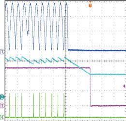
18 FLOW CHART (12) Sar N N N VIN>71V VIN<29.55V VIN>32.75V <VOUT+7.25V Turn On Acive Bleeder N Fas Turn Off Driver of BJT >VOUT+7.95V Turn Off Acive Bleeder N Turn On Driver, IDR STARTUP =19mA >15.25V IDR=2mA N Slowly Turn Off Driver of BJT Turn On LDO Monior Oupu Curren VRT<.8V Monior VRT N TSD=Logic High N Thermal Monior Monior and VOUT IOUT LMT=17mA >VOUT+9V N N N <VOUT+8.1V <7.6V Slowly Turn Off Driver, I B=2mA Slowly Turn On (13) Driver, I B=2mA Turn Off LDO UVLO, OTP, Vo SCP, OLP Proecion are auo resar Noes: 12) The parameers in he flow char refer o he 12V oupu volage. 13) The slowly urn on only happens when VIN is from high volage o low volage hrough VIN slow urn on hreshold while is lower han is urn on hreshold. MP13 Rev
19 EVOLUTION OF THE SIGNALS IN THE PRESENCE OF FAULTS Sar Up OVP Unplug from Main Inpu Normal OLP Occurs Operaion OTP Occurs Normal operaion PKLMT THOUT BLDON UVLO IDR 2mA 19mA VOUT Acive Bleeder On Faul/ Evens Off peak Regulaion OLP Occurs OTP or TSD Faul Occurs MP13 Rev
20 PACKAGE INFORMATION SOIC8E NOTICE: The informaion in his documen is subjec o change wihou noice. Users should warran and guaranee ha hird pary Inellecual Propery righs are no infringed upon when inegraing MPS producs ino any applicaion. MPS will no assume any legal responsibiliy for any said applicaions. MP13 Rev
21 Mouser Elecronics Auhorized Disribuor Click o View Pricing, Invenory, Delivery & Lifecycle Informaion: Monolihic Power Sysems (MPS): MP13GN MP13GN-Z
ORDER INFORMATION TO pin 320 ~ 340mV AMC7150DLF
 www.addmek.com DESCRIPTI is a PWM power ED driver IC. The driving curren from few milliamps up o 1.5A. I allows high brighness power ED operaing a high efficiency from 4Vdc o 40Vdc. Up o 200KHz exernal
Primary Side Control SMPS with Integrated MOSFET
 General Descripion GG64 is a primary side conrol SMPS wih an inegraed MOSFET. I feaures programmable cable drop compensaion and a peak curren compensaion funcion, PFM echnology, and a CV/CC conrol loop
CURRENT MODE PWM+PFM CONTROLLER WITH BUILT-IN HIGH VOLTAGE MOSFET
 CURRENT MODE PWM+PFM CONTROLLER WITH BUILT-IN HIGH VOLTAGE MOSFET DESCRIPTION SD6835 is curren mode PWM+PFM conroller used for SMPS wih buil-in high-volage MOSFET and exernal sense resisor. I feaures low
MX6895BETR. -550V Full Bridge Gate Driver INTEGRATED CIRCUITS DIVISION. Features. Description. Applications. Ordering Information
 -550V Full Bridge Gae Driver INTEGRATED CIRCUITS DIVISION Feaures Full Bridge Gae Driver Inernal High Volage Level Shif Funcion Negaive 550V Lamp Supply Volage 3V o 12V CMOS Logic Compaible 8V o 12V Inpu
GG6005. General Description. Features. Applications DIP-8A Primary Side Control SMPS with Integrated MOSFET
 General Descripion GG65 is a primary side conrol PSR SMPS wih an inegraed MOSFET. I feaures a programmable cable drop compensaion funcion, PFM echnology, and a CV/CC conrol loop wih high reliabiliy and
LD7830H 06/27/2012. High Power Factor Flyback LED Controller with HV Start-up. Features. General Description. Applications. Typical Application
 06/27/2012 High Power Facor Flyback LED Conroller wih HV Sar-up Rev: 00 General Descripion The LD7830H is a HV sar-up Flyback PFC conroller, specially designed for LED lighing appliances. I operaes in
LD7539H 12/24/2012. Green-Mode PWM Controller with BNO and OTP Protections. General Description. Features. Applications. Typical Application. Rev.
 12/24/2012 Green-Mode PWM Conroller wih BNO and OTP Proecions Rev. 00 General Descripion The LD7539H is buil-in wih several funcions, proecion and EMI-improved soluion in a iny package. I akes less componens
PROFET BTS 736 L2. Smart High-Side Power Switch Two Channels: 2 x 40mΩ Status Feedback
 PROFET BTS 736 2 Smar igh-side Power Swich Two Channels: 2 x 40mΩ Saus Feedback Produc Summary Package Operaing olage bb(on) 4.75...41 Acive channels one wo parallel On-sae Resisance R ON 40mΩ 20mΩ Nominal
Ultracompact 6-Channel Backlight and Flash/Torch White LED Driver
 Feaures and Benefis Proprieary adapive conrol scheme (1, 1.5, 2 ) 0.5% ypical LED curren maching 2 separae serial inerfaces for dimming conrol Drives up o 6 whie LEDs (4 display backligh, 2 flash/orch)
PRM and VTM Parallel Array Operation
 APPLICATION NOTE AN:002 M and V Parallel Array Operaion Joe Aguilar VI Chip Applicaions Engineering Conens Page Inroducion 1 High-Level Guidelines 1 Sizing he Resisor 4 Arrays of Six or More Ms 5 Sysem
Obsolete Product(s) - Obsolete Product(s)
 - Obsolete Product(s)") DUAL SWITCH-MODE SOLENOID DRIER HIGH CURRENT CAPABILITY (up o.5a per channel) HIGH OLTAGE OPERATI (up o 46 for power sage) HIGH EFFICIENCY SWITCHMODE OPERATI REGULATED OUTPUT CURRENT (adjusable) FEW EXTERNAL
DUAL SWITCH-MODE SOLENOID DRIER HIGH CURRENT CAPABILITY (up o.5a per channel) HIGH OLTAGE OPERATI (up o 46 for power sage) HIGH EFFICIENCY SWITCHMODE OPERATI REGULATED OUTPUT CURRENT (adjusable) FEW EXTERNAL
LD7516C 08/31/2016. Primary Side Quasi-Resonant Controller. Features. General Description. Applications. Typical Application REV.
 REV. 01 General Descripion Primary ide Quasi-Resonan Conroller The is an excellen primary side feedback MO conroller wih CV/CC operaion, inegraed wih several funcions of proecions. I minimizes he componen
Smart High-Side Power Switch Two Channels: 2 x 30mΩ Current Sense
 POFET Smar High-Side Power Swich Two Channels: 2 x 3mΩ Curren Sense Produc Summary Package Operaing olage (on) 5...34 Acive channels one wo parallel On-sae esisance ON 3mΩ 15mΩ Nominal load curren (NOM)
Discontinued Product
 Disconinued Produc This device is no longer in producion. The device should no be purchased for new design applicaions. Samples are no longer available. Dae of saus change: November 1, 2010 Recommended
Control circuit for a Self-Oscillating Power Supply (SOPS) TDA8385
 TDA8385") FEATURES Bandgap reference generaor Slow-sar circuiry Low-loss peak curren sensing Over-volage proecion Hyseresis conrolled sand-by funcion Error amplifier wih gain seing Programmable ransfer characer
FEATURES Bandgap reference generaor Slow-sar circuiry Low-loss peak curren sensing Over-volage proecion Hyseresis conrolled sand-by funcion Error amplifier wih gain seing Programmable ransfer characer
TEA2019 CURRENT MODE SWITCHING POWER SUPPLY CONTROL CIRCUIT DIRECT DRIVE OF THE EXTERNAL SWITCHING TRANSISTOR POSITIVE AND NEGATIVE OUTPUT CUR-
 CURRENT MODE SWITCHING POWER SUPPLY CONTROL CIRCUIT DIRECT DRIVE OF THE EXTERNAL SWITCHING TRANSISTOR POSITIVE AND NEGATIVE OUTPUT CUR- RENTS UP TO 05A CURRENT LIMITATION TRANSFORMER DEMAGNETIZATION AND
LD7515L 8/5/2015. Primary Side Quasi-Resonant BJT Controller with CV/CC Operation. Features. General Description. Applications. Typical Application
 Primary ide Quasi-esonan BJT Conroller wih CV/CC Operaion EV. 00 General Descripion The is an excellen primary side feedback BJT conroller wih CV/CC operaion, inegraed wih several funcions of proecions.
= f 8 f 2 L C. i C. 8 f C. Q1 open Q2 close (1+D)T DT 2. i C = i L. Figure 2: Typical Waveforms of a Step-Down Converter.
T DT 2. i C = i L. Figure 2: Typical Waveforms of a Step-Down Converter.") Inroducion Oupu Volage ipple in Sep-Down and Sep-Up Swiching egulaors Oupu volage ripple is always an imporan performance parameer wih DC-DC converers. For inducor-based swiching regulaors, several key
Inroducion Oupu Volage ipple in Sep-Down and Sep-Up Swiching egulaors Oupu volage ripple is always an imporan performance parameer wih DC-DC converers. For inducor-based swiching regulaors, several key
Programmable DC Electronic Loads 8600 Series
 Daa Shee Programmable DC Elecronic Loads The programmable DC elecronic loads provide he performance of modular sysem DC elecronic loads in a compac benchop form facor. Wih fas ransien operaion speeds and
PI90LV9637. LVDS High-Speed Differential Line Receivers. Features. Description. Applications PI90LV9637
 LVDS High-Speed Differenial Line Receivers Feaures Signaling Raes >400Mbps (200 MHz) Single 3.3V Power Supply Design Acceps ±350mV (ypical) Differenial Swing Maximum Differenial Skew of 0.35ns Maximum
Application Note 5324
 Desauraion Faul Deecion Opocoupler Gae Drive Producs wih Feaure: PLJ, PL0J, PLJ, PL1J and HCPLJ Applicaion Noe 1. Inroducion A desauraion faul deecion circui provides proecion for power semiconducor swiches
Explanation of Maximum Ratings and Characteristics for Thyristors
 8 Explanaion of Maximum Raings and Characerisics for Thyrisors Inroducion Daa shees for s and riacs give vial informaion regarding maximum raings and characerisics of hyrisors. If he maximum raings of
Programmable DC Electronic Load 8600 Series
 Daa Shee Programmable DC Elecronic Load The programmable DC elecronic loads provide he performance of modular sysem DC elecronic loads in a compac benchop form facor. Wih fas ransien operaion speeds and
AOZ7111. Critical Conduction Mode PFC Controller. Features. General Description. Applications. Typical Application AOZ7111
 Criical Conducion Mode PFC Conroller General Descripion The AOZ7111 is an acive power facor correcion (PFC) conroller for boos PFC applicaions ha operae in criical conducion mode (CRM). The device uses
HI-8585, HI ARINC 429 Line Driver PIN CONFIGURATION DESCRIPTION SUPPLY VOLTAGES FUNCTION TABLE FEATURES PIN DESCRIPTION TABLE
 February DESCRIPTION The HI-8585 and HI-858 are CMOS inegraed circuis designed o direcly drive he ARINC 49 bus in an 8-pin package. Two logic inpus conrol a differenial volage beween he oupu pins producing
Table of Contents. 3.0 SMPS Topologies. For Further Research. 3.1 Basic Components. 3.2 Buck (Step Down) 3.3 Boost (Step Up) 3.4 Inverter (Buck/Boost)
 3.3 Boost (Step Up) 3.4 Inverter (Buck/Boost)") Table of Conens 3.0 SMPS Topologies 3.1 Basic Componens 3.2 Buck (Sep Down) 3.3 Boos (Sep Up) 3.4 nverer (Buck/Boos) 3.5 Flyback Converer 3.6 Curren Boosed Boos 3.7 Curren Boosed Buck 3.8 Forward Converer
Table of Conens 3.0 SMPS Topologies 3.1 Basic Componens 3.2 Buck (Sep Down) 3.3 Boos (Sep Up) 3.4 nverer (Buck/Boos) 3.5 Flyback Converer 3.6 Curren Boosed Boos 3.7 Curren Boosed Buck 3.8 Forward Converer
Programmable DC Electronic Loads 8600 Series
 Daa Shee Programmable DC Elecronic Loads 99 Washingon Sree Melrose, MA 02176 Phone 781-665-1400 Toll Free 1-800-517-8431 Visi us a www.tesequipmendepo.com 2U half-rack 3U 6U USB RS232 GPIB The programmable
Application Note AN-1083
 Applicaion Noe AN-1083 Feaures of he Low-Side Family IPS10xx By Fabio Necco, Inernaional Recifier Table of Conens Page Inroducion...1 Diagnosis...1 Inpu Curren vs. Temperaure...1 Selecion of he Resisor
 Disribued by: www.jameco.com 1-800-831-4242 The conen and copyrighs of he aached maerial are he propery of is owner. 16K-Bi CMOS PARALLEL E 2 PROM FEATURES Fas Read Access Times: 200 ns Low Power CMOS
Solid-state Timer H3CT
 Solid-sae Timer H3CT DIN 48 x 48-mm Sandard Size Analog Timer Wide ime range (for 4 series of models); 0.1 s o 30 hrs. Wih H3CT-8H models, he oupu ype can be swiched beween ime limi DPDT and ime limi SPDT
Step Down Voltage Regulator with Reset TLE 6365
 Sep Down Volage Regulaor wih Rese TLE 6365 Feaures Sep down converer Supply Over- and Under-Volage-Lockou Low Oupu volage olerance Oupu Overvolage Lockou Oupu Under-Volage-Rese wih delay Overemperaure
VIPer12ADIP / VIPer12AS
 VIPer2ADIP / VIPer2AS OFF LINE BATTERY CHARGER ADAPTER TARGET SPECIFICATION TYPE R DS(on) I N V DSS VIPer2ADIP VIPer2AS 30Ω 0.36A 730V n FIXED 50 khz SWITCHING FREQUENCY n 8V TO 40V WIDE RANGE VOLTAGE
Package. Applications
 Primary-side Regulaion PWM Conroller for Auomoive Applicaions SFA2 Daa Shee Descripion The SFA2 is he swiching power supply IC for flyback circui and has high accuracy error amplifier. When he load of
AN303 APPLICATION NOTE
 AN303 APPLICATION NOTE LATCHING CURRENT INTRODUCTION An imporan problem concerning he uilizaion of componens such as hyrisors or riacs is he holding of he componen in he conducing sae afer he rigger curren
Design of Power Factor Correction Circuit Using AP1662
 Applicaion Noe 075 Design of Power Facor Correcion Circui Using AP66 Prepared by Wang Zhao Kun ysem Engineering Deparmen. nroducion. Produc Feaures The AP66 is an acive power facor conrol C which is designed
Solid-state Multi-functional Timer
 Solid-sae Muli-funcional Timer Eigh operaing modes (H3DE-M) and four operaing modes (H3DE-S) cover a wide range of applicaions. Programmable conac enables he building of a self-holding relay circui (-
P. Bruschi: Project guidelines PSM Project guidelines.
 Projec guidelines. 1. Rules for he execuion of he projecs Projecs are opional. Their aim is o improve he sudens knowledge of he basic full-cusom design flow. The final score of he exam is no affeced by
Version 2.1, 6 May 2011
 Version 2.1, 6 May 2011 Off-Line SMPS Curren Mode Conroller wih inegraed 650V CoolMOS and Sarup cell (frequency jier Mode) in FullPak Power Managemen & Supply N e v e r s o p h i n k i n g. Revision Hisory:
4 20mA Interface-IC AM462 for industrial µ-processor applications
 Because of he grea number of indusrial buses now available he majoriy of indusrial measuremen echnology applicaions sill calls for he sandard analog curren nework. The reason for his lies in he fac ha
AK8777B. Overview. Features
 AK8777B Hall Effec IC for Pulse Encoders Overview The AK8777B is a Hall effec lach which deecs boh verical and horizonal (perpendicular and parallel o he marking side of he package) magneic field a he
A1 K. 12V rms. 230V rms. 2 Full Wave Rectifier. Fig. 2.1: FWR with Transformer. Fig. 2.2: Transformer. Aim: To Design and setup a full wave rectifier.
 2 Full Wave Recifier Aim: To Design and seup a full wave recifier. Componens Required: Diode(1N4001)(4),Resisor 10k,Capacior 56uF,Breadboard,Power Supplies and CRO and ransformer 230V-12V RMS. + A1 K B1
DATA SHEET. 1N914; 1N916 High-speed diodes DISCRETE SEMICONDUCTORS Sep 03
 DISCRETE SEMICONDUCTORS DATA SHEET M3D176 Supersedes daa of April 1996 File under Discree Semiconducors, SC01 1996 Sep 03 FEATURES Hermeically sealed leaded glass SOD27 (DO-35) package High swiching speed:
Investigation and Simulation Model Results of High Density Wireless Power Harvesting and Transfer Method
 Invesigaion and Simulaion Model Resuls of High Densiy Wireless Power Harvesing and Transfer Mehod Jaber A. Abu Qahouq, Senior Member, IEEE, and Zhigang Dang The Universiy of Alabama Deparmen of Elecrical
Installation and Operating Instructions for ROBA -brake-checker Typ
 (B.018102.EN) Guidelines on he Declaraion of Conformiy A conformiy evaluaion has been carried ou for he produc in erms of he EC Low Volage Direcive 2006/95/ EC and EMC Direcive 2004/108/EC. The Declaraion
M2 3 Introduction to Switching Regulators. 1. What is a switching power supply? 2. What types of switchers are available?
 M2 3 Inroducion o Swiching Regulaors Objecive is o answerhe following quesions: 1. Wha is a swiching power supply? 2. Wha ypes of swichers are available? 3. Why is a swicher needed? 4. How does a swicher
Electronic timer CT-MVS.12 Multifunctional with 1 c/o contact Data sheet
 Feaures Raed conrol supply volage 24-48 V DC, 24-240 V AC Mulifuncion imer wih 10 iming funcions: ON-delay, OFF-delay wih auxiliary volage, Impulse-ON, Impulse-OFF wih auxiliary volage, Symmerical ON-
Synchronization of single-channel stepper motor drivers reduces noise and interference
 hronizaion of single-channel sepper moor drivers reduces noise and inerference n mos applicaions, a non-synchronized operaion causes no problems. However, in some cases he swiching of he wo channels inerfere,
The ramp is normally enabled but can be selectively disabled by suitable wiring to an external switch.
 Vickers Amplifier Cards Power Amplifiers for Proporional Valves EEA-PAM-56*-A-14 Design EEA-PAM-561-A-14 for use wih valve ypes: KDG5V-5, * and KDG5V-7, 1* series EEA-PAM-568-A-14 for use wih valve ypes:
A6211 Constant-Current 3-Ampere PWM Dimmable Buck Regulator LED Driver
 Feaures and Benefis Supply volage 6 o 48 V True average oupu curren conrol 3.0 A maximum oupu over operaing emperaure range Cycle-by-cycle curren limi Inegraed MOSFET swich Dimming via direc logic inpu
Infineon Power LED Driver TLD5045EJ. Datasheet. Automotive Power. 700mA High Integration - DC/DC Step- Down Converter. Rev. 1.
 Infineon Power LED Driver TLD5045EJ 700mA High Inegraion - DC/DC Sep- Down Converer Daashee Rev. 1.0, 2011-05-27 Auomoive Power Table of Conens Table of Conens Table of Conens................................................................
IR Sensor Module for Reflective Sensor, Light Barrier, and Fast Proximity Applications
 IR Sensor Module for Reflecive Sensor, Ligh Barrier, and Fas Proximiy Applicaions 2 3 DESIGN SUPPORT TOOLS 6672 click logo o ge sared FEATURES Up o 2 m for presence and proximiy sensing Uses modulaed burss
IR Sensor Module for Reflective Sensor, Light Barrier, and Fast Proximity Applications
 IR Sensor Module for Reflecive Sensor, Ligh Barrier, and Fas Proximiy Applicaions 2 3 DESIGN SUPPORT TOOLS Models Available MECHANICAL DATA Pinning: = OUT, 2 = GND, 3 = V S click logo o ge sared 6672 APPLICATIONS
PROFET BTS 840 S2. Smart High-Side Power Switch Two Channels: 2 x 30mΩ Current Sense
 nfineon echnologies 1 of 15 23-Oc-1 查询 BTS84S2 供应商 捷多邦, 专业 PCB 打样工厂,24 小时加急出货 POFET Smar High-Side Power Swich Two Channels: 2 x 3mΩ Curren Sense Produc Summary Package Operaing olage (on) 5...34 Acive
Impacts of the dv/dt Rate on MOSFETs Outline:
 Ouline: A high dv/d beween he drain and source of he MOSFET may cause problems. This documen describes he cause of his phenomenon and is counermeasures. Table of Conens Ouline:... 1 Table of Conens...
4.5 Biasing in BJT Amplifier Circuits
 4/5/011 secion 4_5 Biasing in MOS Amplifier Circuis 1/ 4.5 Biasing in BJT Amplifier Circuis eading Assignmen: 8086 Now le s examine how we C bias MOSFETs amplifiers! f we don bias properly, disorion can
<IGBT Modules> CM900DUC-24S HIGH POWER SWITCHING USE INSULATED TYPE
 dual swich (Half-Bridge) Collecor curren I C...... 9 A Collecor-emier volage CES... 1 2 Maximum juncion emperaure T j m a x... 1 7 5 C Fla base Type Copper base plae (non-plaing) RoHS Direcive complian
VIPER28. Off-line high voltage converters. Features. Description. Application
 Off-line high volage converers Feaures 800 V avalanche rugged power secion PWM operaion wih frequency jiering for low EMI Operaing frequency: 60 khz for L ype 115 khz for H ype Sandby power < 50 mw a 265
< IGBT MODULES > CM600DU-12NFH HIGH POWER HIGH FREQUENTLY SWITCHING USE INSULATED TYPE
 Dual (Half-Bridge) Collecor curren I C...... 6A Collecor-emier volage CES... 6 Maximum juncion emperaure T jmax... 5 C Fla base Type Copper base plae RoHS Direcive complian UL Recognized under UL557, File
AN UVLO (Under Voltage Lock Out) FUNCTION Calculation of Minimum Value of IGBT external Gate Resistance RG. Table 2-1.
 FUNCTION Calculation of Minimum Value of IGBT external Gate Resistance RG. Table 2-1.") A p p l i c a i o n Noe AN318 IGBT/Power MOSFET Gae Drive Phoocoupler Technical Markeing Deparmen Compound Semiconducor Devices Business Division Analog & Power Devices Business Uni Renesas Elecronics
A p p l i c a i o n Noe AN318 IGBT/Power MOSFET Gae Drive Phoocoupler Technical Markeing Deparmen Compound Semiconducor Devices Business Division Analog & Power Devices Business Uni Renesas Elecronics
General data 8/91. Overview
 SIRIUS 3RS0, 3RS, 3RS0, 3RS Temperaure Monioring Relays General daa Overview Temperaure seing LED "Device on volage" LED "Relay swiched" Hyseresis swich NSB0_04a LED for display "Up and Down" keys Roary
Wind power, Photovoltaic (Solar) power, AC Motor Control, Motion/Servo Control, Power supply, etc. OUTLINE DRAWING & INTERNAL CONNECTION
 power, AC Motor Control, Motion/Servo Control, Power supply, etc. OUTLINE DRAWING & INTERNAL CONNECTION") Collecor curren I C...... 18A Collecor-emier volage CES... 17 Maximum juncion emperaure T jmax... 175 C Fla base Type Aluminum base plae RoHS Direcive compliance Dual swich (Half-Bridge) Recognized under
Collecor curren I C...... 18A Collecor-emier volage CES... 17 Maximum juncion emperaure T jmax... 175 C Fla base Type Aluminum base plae RoHS Direcive compliance Dual swich (Half-Bridge) Recognized under
<Diode Modules> RM200CY-24S HIGH POWER SWITCHING USE INSULATED TYPE
 dual swich (Cahode Common) Forward curren...... 2 0 0 A Repeiive peak reverse volage V RRM... 1 2 0 0 V Maximum juncion emperaure T jmax... 1 5 0 C Fla base Type Copper base plae RoHS Direcive
 - MPD series using 5 h Generaion IGBT and FWDi - I C.... 4 A CES....... 2 Fla base Type Copper (non-plaing) base plae RoHS Direcive complian Dual swich (Half-Bridge) UL Recognized under UL557, File E323585
SCiCoreDrive62 +DC T5 U V W -DC. SCiCore 62. IGBT/MOSFET drivers
 PRELIMINARY TECHNICAL INFORMATION SCiCoreDrive62 IGBT/MOSFET drivers HIGHLIGHTS - 6 channel IGBT driver - suiable for 200V IGBT (900 V max on DCLink) - Up o 8 A peak oupu curren - Collecor sensing & faul
< IGBT MODULES > CM450DY-24S HIGH POWER SWITCHING USE INSULATED TYPE APPLICATION
 Dual (Half-Bridge) Collecor curren I C...... 4A * Collecor-emier volage CES... 2 Maximum juncion emperaure T jmax... 75 C Fla base Type Copper base plae RoHS Direcive compliance UL Recognized under UL557,
APPLICATION. CM150DUS-12F - 4 th generation Fast switching IGBT module - MITSUBISHI IGBT MODULES CM150DUS-12F HIGH POWER SWITCHING USE INSULATED TYPE
 CM5DUS-2F CM5DUS-2F - 4 h generaion Fas swiching IGBT module - Collecor curren I C...... 5A Collecor-emier volage CES... 6 Maximum juncion emperaure T jmax... 5 C Fla base Type Copper base plae RoHS Direcive
EXPERIMENT #4 AM MODULATOR AND POWER AMPLIFIER
 EXPERIMENT #4 AM MODULATOR AND POWER AMPLIFIER INTRODUCTION: Being able o ransmi a radio frequency carrier across space is of no use unless we can place informaion or inelligence upon i. This las ransmier
IR Receiver Module for Light Barrier Systems
 IR Receiver Module for Ligh Barrier Sysems TSSP4..SSXB Vishay Semiconducors DESIGN SUPPORT TOOLS Models Available 3 MECHANICAL DATA Pinning: = OUT, = GND, 3 = V S 7 click logo o ge sared DESCRIPTION The
Connection. Input II EEx ia IIC without SC red. Composition
 Sandsill conroller Oupu: relay Connecion Inpu I EEx ia IIC Inpu II EEx ia IIC 1-channel Conrol circui EEx ia IIC Addiional inpu or roaion direcion deecion or sar-up override 2 relay oupus Inpu requency
Phase-Shifting Control of Double Pulse in Harmonic Elimination Wei Peng1, a*, Junhong Zhang1, Jianxin gao1, b, Guangyi Li1, c
 Inernaional Symposium on Mechanical Engineering and Maerial Science (ISMEMS 016 Phase-Shifing Conrol of Double Pulse in Harmonic Eliminaion Wei Peng1, a*, Junhong Zhang1, Jianxin gao1, b, Guangyi i1, c
Diode RapidSwitchingEmitterControlledDiode. IDV30E65D2 EmitterControlledDiode. Datasheet. IndustrialPowerControl
 Diode RapidSwichingEmierConrolledDiode EmierConrolledDiode Daashee IndusrialPowerConrol EmierConrolledDiode RapidSwichingEmierConrolledDiode Feaures: QualifiedaccordingoJEDECforargeapplicaions 6VEmierConrolledechnology
MX629. DELTA MODULATION CODEC meets Mil-Std DATA BULLETIN. Military Communications Multiplexers, Switches, & Phones
 DATA BULLETIN MX629 DELTA MODULATION CODEC mees Mil-Sd-188-113 Feaures Mees Mil-Sd-188-113 Single Chip Full Duplex CVSD CODEC On-chip Inpu and Oupu Filers Programmable Sampling Clocks 3- or 4-bi Companding
< IGBT MODULES > CM100DY-34A HIGH POWER SWITCHING USE INSULATED TYPE APPLICATION
 CMDY-34A Dual (Half-Bridge) Collecor curren I C...... A Collecor-emier volage CES... 7 Maximum juncion emperaure T jmax... 5 C Fla base Type Copper base plae RoHS Direcive complian UL Recognized under
Proceedings of International Conference on Mechanical, Electrical and Medical Intelligent System 2017
 on Mechanical, Elecrical and Medical Inelligen Sysem 7 Consan On-ime Conrolled Four-phase Buck Converer via Saw-oohwave Circui and is Elemen Sensiiviy Yi Xiong a, Koyo Asaishi b, Nasuko Miki c, Yifei Sun
COMBITRON Program Schedule
 OMBITRO Program Schedule OMBITRO are supply and acuaor modules for he elecromagne cluches and brakes. As power supply for D- or A-side swiching differen single-wave and bridge recifiers as well as rapid
Three phase full Bridge with Trench MOSFETs in DCB isolated high current package
 MTI2WX75GD Three phase full Bridge wih Trench MOSFETs in DCB isolaed high curren package S = 75 V 25 = 255 R DSon yp. = 1.1 mw Par number MTI2WX75GD G1 L1+ L2+ T1 T3 T5 G3 G5 L3+ Surface Moun Device S1
IR Receiver Module for Light Barrier Systems
 New Produc IR Receiver Module for Ligh Barrier Sysems TSSP5838 1926 FEATURES Low supply curren Phoo deecor and preamplifier in one package Inernal filer for 38 khz IR signals Shielding agains EMI Supply
PRELIMINARY N-CHANNEL MOSFET 1 P-CHANNEL MOSFET. Top View
 HEXFET Power MOSFET dvanced Process Technology Ulra Low On-Resisance ual N and P Channel Mosfe Surface Moun vailable in Tape & Reel ynamic dv/d Raing Fas Swiching escripion PRELIMINRY N-CHNNEL MOSFET 8
HR1001L Enhanced LLC Controller with Adaptive Dead-Time Control
 HR1001L Enhanced LLC Conroller wih Adapive Dead-Time Conrol DESCRIPTIO The HR1001L is an enhanced LLC conroller ha provides new, adapive, dead-ime adjusmen (ADTA) and capaciive mode proecion (CMP) feaures.
A8502 Wide Input Voltage Range, High Efficiency Fault Tolerant LED Driver
 FEATURES AND BENEFITS AEC-Q100 qualified Wide inpu volage range of 5 o 40 V for sar/sop, cold crank and load dump requiremens Fully inegraed LED curren sinks and boos converer wih 60 V DMOS Sync funcion
Wind power, Photovoltaic (Solar) power, AC Motor Control, Motion/Servo Control, Power supply, etc. OUTLINE DRAWING & INTERNAL CONNECTION
 power, AC Motor Control, Motion/Servo Control, Power supply, etc. OUTLINE DRAWING & INTERNAL CONNECTION") CMDUC-34SA Dual swich (Half-Bridge) Collecor curren I C...... A Collecor-emier volage CES... 17 Maximum juncion emperaure T jmax... 175 C Fla base Type Copper base plae (non-plaing) RoHS Direcive compliance
CMDUC-34SA Dual swich (Half-Bridge) Collecor curren I C...... A Collecor-emier volage CES... 17 Maximum juncion emperaure T jmax... 175 C Fla base Type Copper base plae (non-plaing) RoHS Direcive compliance
Power Amplifier EEA-PAM-5**-A-32 for Proportional Control Valves Contents The following power amplifier models are covered in this catalog
 Vickers Accessories Power Amplifier EEA-PAM-5**-A-32 for Proporional Conrol Valves Conens The following power amplifier models are covered in his caalog Power Amplifier EEA-PAM-513-A-32 EEA-PAM-523-A-32
Development of Temporary Ground Wire Detection Device
 Inernaional Journal of Smar Grid and Clean Energy Developmen of Temporary Ground Wire Deecion Device Jing Jiang* and Tao Yu a Elecric Power College, Souh China Universiy of Technology, Guangzhou 5164,
Diode RapidSwitchingEmitterControlledDiode. IDP20C65D2 EmitterControlledDiodeRapid2CommonCathodeSeries. Datasheet. IndustrialPowerControl
 Diode RapidSwichingEmierConrolledDiode IDP20C65D2 EmierConrolledDiodeRapid2CommonCahodeSeries Daashee IndusrialPowerConrol EmierConrolledDiodeRapid2CommonCahodeSeries RapidSwichingEmierConrolledDiode Feaures:
Fixed-Frequency, 800V CoolSET in DS0-12 Package
 ICE3AR1080JG Fixed-Frequency, 800V CoolSET in DS0-12 Package Produc Highlighs 800 V avalanche rugged CoolMOS wih sarup cell Acive Burs Mode o reach he lowes Sandby Power
CoolSET -F3R80 ICE3AR4780CJZ. Off-Line SMPS Current Mode Controller with integrated 800V CoolMOS and Startup cell (brownout & CCM) in DIP-7
 in DIP-7") Version 2.0, 19 Apr 2013 CoolSET -F3R80 Off-Line SMPS Curren Mode Conroller wih inegraed 800V CoolMOS and Sarup cell (brownou & CCM) in DIP-7 Power Managemen & Supply Never sop hinking. Revision Hisory:
Version 2.0, 19 Apr 2013 CoolSET -F3R80 Off-Line SMPS Curren Mode Conroller wih inegraed 800V CoolMOS and Sarup cell (brownou & CCM) in DIP-7 Power Managemen & Supply Never sop hinking. Revision Hisory:
Diodes. Diodes, Page 1
 Diodes, Page 1 Diodes V-I Characerisics signal diode Measure he volage-curren characerisic of a sandard signal diode, he 1N914, using he circui shown below. The purpose of he back-o-back power supplies
Not Recommend. for New Design < IGBT MODULES > CM1400DUC-24NF HIGH POWER SWITCHING USE INSULATED TYPE APPLICATION
 dual swich (Half-Bridge) Collecor curren I C...... 1 4 A Collecor-emier volage CES... 1 2 Maximum juncion emperaure T jmax... 1 5 C Fla base Type Copper base plae (non-plaing) RoHS Direcive complian Recognized
<IGBT Modules> CM450DY-24S HIGH POWER SWITCHING USE INSULATED TYPE
 dual swich (Half-Bridge) Collecor curren I C...... 4 1 A * Collecor-emier volage CES... 1 2 Maximum juncion emperaure T jmax... 1 7 5 C Fla base Type Copper base plae RoHS Direcive complian UL Recognized
EE 330 Lecture 24. Amplification with Transistor Circuits Small Signal Modelling
 EE 330 Lecure 24 Amplificaion wih Transisor Circuis Small Signal Modelling Review from las ime Area Comparison beween BJT and MOSFET BJT Area = 3600 l 2 n-channel MOSFET Area = 168 l 2 Area Raio = 21:1
Wind power, Photovoltaic (Solar) power, AC Motor Control, Motion/Servo Control, Power supply, etc. OUTLINE DRAWING & INTERNAL CONNECTION
 power, AC Motor Control, Motion/Servo Control, Power supply, etc. OUTLINE DRAWING & INTERNAL CONNECTION") Dual swich (Half-Bridge) Collecor curren I C...... 14A Collecor-emier volage CES... 12 Maximum juncion emperaure T jmax... 175 C Fla base Type Copper base plae (non-plaing) RoHS Direcive complian UL Recognized
Dual swich (Half-Bridge) Collecor curren I C...... 14A Collecor-emier volage CES... 12 Maximum juncion emperaure T jmax... 175 C Fla base Type Copper base plae (non-plaing) RoHS Direcive complian UL Recognized
Diode FastSwitchingEmitterControlledDiode. IDW50E60 EmitterControlledDiodeseries. Datasheet. IndustrialPowerControl
 Diode FasSwichingEmierConrolledDiode IDW5E6 EmierConrolledDiodeseries Daashee IndusrialPowerConrol IDW5E6 EmierConrolledDiodeseries FasSwichingEmierConrolledDiode Feaures: QualifiedaccordingoJEDECforargeapplicaions
IR Receiver Module for Light Barrier Systems
 IR Receiver Module for Ligh Barrier Sysems DESIGN SUPPORT TOOLS 19026 click logo o ge sared FEATURES Up o 2 m for presence sensing Uses modulaed burss a 38 khz 940 nm peak wavelengh PIN diode and sensor
Infineon LITIX TM Basic TLD1125EL. Data Sheet. Automotive. 1 Channel High Side Current Source. Rev. 1.1,
 Infineon LITIX TM Basic TLD1125EL 1 Channel High Side Curren Source Daa Shee Rev. 1.1, 2015-03-19 Auomoive 1 Overview....................................................................... 3 2 Block Diagram...................................................................
TLE7257. Data Sheet. Automotive Power. LIN Transceiver TLE7257SJ TLE7257LE. Rev. 1.1,
 LIN Transceiver TLE7257SJ TLE7257LE Daa Shee Rev. 1.1, 2015-08-20 Auomoive Power Table of Conens 1 Overview....................................................................... 3 2 Block Diagram...................................................................
Series SHDC Output: 40A,100 Vdc and 20A,200 Vdc High Industrial Performance (HIPpak) DC Solid-State Relays
 DC Solid-State Relays") Oupu: 4A,1 Vdc and 2A,2 Vdc FEATURES/BENEFITS Laes generaion MOSFET echnology Ulra low on-sae resisance Low oupu leakage curren Buil-in overvolage proecion Reverse proeced riggered conrol inpu o avoid
Oupu: 4A,1 Vdc and 2A,2 Vdc FEATURES/BENEFITS Laes generaion MOSFET echnology Ulra low on-sae resisance Low oupu leakage curren Buil-in overvolage proecion Reverse proeced riggered conrol inpu o avoid
HRF32. Silicon Schottky Barrier Diode for Rectifying. ADE D(Z) Rev 4 Jul Features. Ordering Information. Outline
 Rev 4 Jul Features. Ordering Information. Outline") Silicon Schoky Barrier Diode for Recifying ADE-28-164D(Z) Rev 4 Jul. 1997 Feaures Good for high-frequency recify. LRP srucure ensures higher reliabiliy. Ordering Informaion Type No. Laser Mark Package
Silicon Schoky Barrier Diode for Recifying ADE-28-164D(Z) Rev 4 Jul. 1997 Feaures Good for high-frequency recify. LRP srucure ensures higher reliabiliy. Ordering Informaion Type No. Laser Mark Package
RoHS Directive compliant UL Recognized under UL1557, File E APPLICATION
 - 5 h Generaion NX series - Collecor curren I C...... 3A Collecor-emier volage CES... 6 Maximum juncion emperaure T jmax... 5 C Fla base Type Copper base plae (non-plaing) Dual (Half-Bridge) RoHS Direcive
NCP1239. Fixed Frequency Current Mode Controller for Flyback Converter
 Fixed Frequency Curren Mode Conroller for Flyback Converer The NCP1239 is a fixed-frequency curren-mode conroller feauring a high-volage sar-up curren source o provide a quick and lossless power-on sequence.
Monitoring Technique. VARIMETER Current relay BA 9053, MK 9053N
 Monioring Technique VARIMETER Curren relay, MK 9053N 0221540 Your Advanages Prevenive mainenance For beer produciviy Quicker faul locaing Precise and reliable MK 9053N Opions wih Pluggable Terminal Blocks