2.5GS/s Pipelined ADC with Background. Linearity Correction
|
|
|
- Lee Walton
- 5 years ago
- Views:
Transcription
1 A14b25GS/s8-Way-Interleaved 2.5GS/s Pipelined ADC with Background Calibration and Digital it Dynamic Linearity Correction B. Setterberg 1, K. Poulton 1, S. Ray 1, D.J. Huber 1, V. Abramzon 1, G. Steinbach 1, JP J.P. Keane 1, B. Wuppermann 1, M. Clayson 1, M. Martin 2, R. Pasha 2, E. Peeters 3, A. Jacobs 3, F. Demarsin 3, A. Al-Adnani 3, P. Brandt 3 1 Agilent Technologies, Santa Clara, CA 2 Agilent Technologies, Colorado Springs, CO 3 Agilent Technologies, Rotselaar, Belgium
2 Background ADC for Test and Measurement Applications: 2.5 GS/s 14 bits Less than 1 metastable error per year (10-17 metastable error probability) 75 db SFDR from DC to 1 GHz 60 db SNR Works with arbitrary input signals Silicon BiCMOS Process Technology: 150 GHz f T Bipolar NPN 130 nm CMOS 2
3 Problem: Design Considerations Comparator regeneration time constants are too slow to meet the metastability error rate goals at 25GS/s 2.5 GS/s. Solution: Use a time-interleaved i t dadc architecture. t Consequence: Need to address interleaving artifacts. 3
4 Time-Interleaved ed Architecturere ADC Slice 0 ADC Slice ADC Slice N De-interleave Interleave ADC slices need to be very well matched in offset, gain, sample time and bandwidth. 4
5 Interleaving Strategy Achieve an aggregate 2.5 GS/s by interleaving eight MS/s slices. Input 8X MS/s ADC Slices MS/s ADC 5
6 Slice ADC Architecture In 3.5 bits + Voltage to redundancy current 15-level flash converter Stage 1 Gm 1 bit per stage, radix-1.7 current-mode pipeline 1 Stages Radix Conve erter Binary Output Background Calibration Engine 1 K. Poulton, et al., A 4GSample/s 8b ADC in 0.35µm CMOS, ISSCC Dig. Tech. Papers, vol. 45, pp , Feb
7 ADC First Stage Block Diagram To Radix Converter DAC Permuter CLK IN Dither Permute e Address Background Calibration Engine Residue Amp 7
8 ADC Stages 2-16 D D In Dith 1.7 X In 1.7 X Res Res Stg 2 Stg 3 Stg 11 Stg 12 Stg 16 D D D D D In Res Dith In Res Dith In Res Dith In Res In Background Calibration Engine Uncalibrated Stages 8
9 Interleaving Errors Mismatched paths cause: Distortion and jitter Spurs in the spectrum Gain Error (need < 0.01% gain matching) Offset Error Sampling Instant Error (need < 100 µv offsets) (need < 20 fs timing skew) 9
10 Minimize Sampling Time Errors with a 2-rank Track and Hold Input Rank 1 T/H 2.5GS/s Low- Jitter Sampling Clock (<70 fs RMS) ) 8X MS/s ADC Slices Rank 2 T/H MS/s ADC First rank T/H clocked at full system sample rate Sampling instant defined by first T/H Insensitive to errors from slice-rate clocks 10
11 Slice-to-Slice Gain & Offset Alignment Dither DAC Dither Chop PRBS ADC Ga ain Of ffset Background Calibration Engine Injected dither provides an absolute gain reference Chopping allows offset calibration with arbitrary input 11
12 Chop and Dither Injection M3 R1 R2 M4 Dither Out Bootstrap amplifiers Q1 Q3 Q2 Q4 Chop PRBS In In M1 M2 Liability: Large V ds swings on M3 and M4 induce 0.1% PRBS-modulated thermal transients. 12
13 Chopper Transient Removal Uncorrected transient degrades SNR by 6 db. Transient removed with a poly-phase p fast FIR filter. Foreground self-calibration finds filter coefficients. Dithe er DAC Dither Chop PRBS 8 Slices Chop Filter ADC Background Calibration Engine 13
14 Output MUX Output MUX Dynamic Linearity Corrector 14 ADC Block Diagram Per-slice DSP Chop Filter Gain Radix Converter ADC Chop Offset Dither Dither DAC Dither Chop PRBS Background Calibration Engine
15 Digital Dynamic Linearity Correction Analog circuit nonlinearities include: Nonlinear settling Track switch nonlinearity Signal-modulated aperture time Error characteristics: Functions of signal history Frequency-dependent Partially correctable if we know both the sample and its derivative 15
16 Digital Dynamic Linearity Correction Slope est. filter dx/dt x x Programmable Correction Coefficients Estimate the derivative of the signal. Calculate selected 2 nd - and 3 rd -order products of the signal and its derivative. Calculate the correction as a weighted sum of the product terms. x x Product Term Multipliers ( ) (x ) 2 x 2 x (x ) ( ) 2 x 3 2 x x 2 3 Input x Out 16
17 Slope Estimation Filter Infinitely long impulse response Ideal H(f) ) H(f) = j2πf Practical 0 Fs/2 Truncated impulse response H(f) H(f) j2πf 0 Fs/2 17
18 SFD DR (db B) 95 Dynamic Linearity Corrector Performance (-1 dbfs Input) SFDR with DLC 60 SFDR without DLC Input Frequency (MHz) 18
19 INL with a 450 MHz Input Signal b LS SB) INL ( Code 19
20 Magnit tude (d dbfs) Power Spectrum -1 dbfs at 1052 MHz RBW = 2.44 MHz Without calibration or DLC With calibration and DLC HD2 HD Frequency (MHz) 20
21 (db) SFDR Performance Comparison Time-interleaved i dadcs Published ADCs (ISSCC and VLSI) This work MHz 100MHz 1GHz 10GHz 100GHz Bandwidth Source: B. Murmann, "ADC Performance Survey
22 Power Dissipation by Function Function Power (Watts) 2-Rank Track & Hold 2.5 Clock Distribution and Clock Divider ADC Slices 13.1 Digital Signal Path and DSP 2.6 Background Calibration 2.7 Output Data Ports 1.2 Total 23.9 Interleaving is expensive! 22


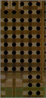


23 Die Photograph 7.4 mm x 14.0 mm SiGe BiCMOS 23
24 Performance Summary Sample Rate 2.5 GS/s Resolution 14 bits Signal to Noise Ratio (SNR), 0dBFS Input 61 db Noise Spectral 2.5 GS/s -152 dbfs/hz Spurious Free Dynamic Range (SFDR) DC - 1 GHz, -1 dbfs Input 78 db INL ±1.5 LSB Sampling Clock Random Jitter 70 fs RMS Metastable Error Rate (extrapolated from <10-17 over-clocking experiments) (<1 error/year) Input Impedance 50 Ω differential Outputs t LVDS Performance maintained with continuous background calibration. 24
25 Summary High performance time-interleaving: 2-rank track and hold Extensive background calibration (224 loops) Background calibrations operate continuously regardless of input signal statistics Digital dynamic linearity correction Results: Highest reported SFDR for a time-interleaved i t ADC Highest reported SFDR at 1 GHz bandwidth 25
26 Acknowledgements The authors thank the following individuals for their valuable contributions to this work: Mauro Berdondini Steven Coenen Lewis Dove Bart Gybels Jeanne Kaneyuki Pete Martinez Brad McCormack Don Pettengill Mike Rytting Jimmy Storie Gary Thomas Joseph Tran Ramesh Vema Lynne Viaggi Yunqiang Yang 26
Another way to implement a folding ADC
 Another way to implement a folding ADC J. Van Valburg and R. van de Plassche, An 8-b 650 MHz Folding ADC, IEEE JSSC, vol 27, #12, pp. 1662-6, Dec 1992 Coupled Differential Pair J. Van Valburg and R. van
A 4 GSample/s 8-bit ADC in. Ken Poulton, Robert Neff, Art Muto, Wei Liu, Andrew Burstein*, Mehrdad Heshami* Agilent Laboratories Palo Alto, California
 A 4 GSample/s 8-bit ADC in 0.35 µm CMOS Ken Poulton, Robert Neff, Art Muto, Wei Liu, Andrew Burstein*, Mehrdad Heshami* Agilent Laboratories Palo Alto, California 1 Outline Background Chip Architecture
10.1: A 4 GSample/s 8b ADC in 0.35-um CMOS
 10.1: A 4 GSample/s 8b ADC in 0.35-um CMOS Ken Poulton, Robert Neff, Art Muto, Wei Liu*, Andy Burstein**, Mehrdad Heshami*** Agilent Technologies, Palo Alto, CA *Agilent Technologies, Colorado Springs,
Maximizing GSPS ADC SFDR Performance: Sources of Spurs and Methods of Mitigation
 Maximizing GSPS ADC SFDR Performance: Sources of Spurs and Methods of Mitigation Marjorie Plisch Applications Engineer, Signal Path Solutions November 2012 1 Outline Overview of the issue Sources of spurs
Architectures and circuits for timeinterleaved. Sandeep Gupta Teranetics, Santa Clara, CA
 Architectures and circuits for timeinterleaved ADC s Sandeep Gupta Teranetics, Santa Clara, CA Outline Introduction to time-interleaved architectures. Conventional Sampling architectures and their application
A 10 bit, 1.8 GS/s Time Interleaved Pipeline ADC
 A 10 bit, 1.8 GS/s Time Interleaved Pipeline ADC M. Åberg 2, A. Rantala 2, V. Hakkarainen 1, M. Aho 1, J. Riikonen 1, D. Gomes Martin 2, K. Halonen 1 1 Electronic Circuit Design Laboratory Helsinki University
A 12-bit Interpolated Pipeline ADC using Body Voltage Controlled Amplifier
 A 12-bit Interpolated Pipeline ADC using Body Voltage Controlled Amplifier Hyunui Lee, Masaya Miyahara, and Akira Matsuzawa Tokyo Institute of Technology, Japan Outline Background Body voltage controlled
Asynchronous SAR ADC: Past, Present and Beyond. Mike Shuo-Wei Chen University of Southern California MWSCAS 2014
 Asynchronous SAR ADC: Past, Present and Beyond Mike Shuo-Wei Chen University of Southern California MWSCAS 2014 1 Roles of ADCs Responsibility of ADC is increasing more BW, more dynamic range Potentially
RECENTLY, low-voltage and low-power circuit design
 IEEE TRANSACTIONS ON CIRCUITS AND SYSTEMS II: EXPRESS BRIEFS, VOL. 55, NO. 4, APRIL 2008 319 A Programmable 0.8-V 10-bit 60-MS/s 19.2-mW 0.13-m CMOS ADC Operating Down to 0.5 V Hee-Cheol Choi, Young-Ju
ISSCC 2004 / SESSION 25 / HIGH-RESOLUTION NYQUIST ADCs / 25.3
 ISSCC 2004 / SESSION 25 / HIGH-RESOLUTION NYQUIST ADCs / 25.3 25.3 A 96dB SFDR 50MS/s Digitally Enhanced CMOS Pipeline A/D Converter K. Nair, R. Harjani University of Minnesota, Minneapolis, MN Analog-to-digital
ISSCC 2004 / SESSION 25 / HIGH-RESOLUTION NYQUIST ADCs / 25.4
 ISSCC 2004 / SESSION 25 / HIGH-RESOLUTION NYQUIST ADCs / 25.4 25.4 A 1.8V 14b 10MS/s Pipelined ADC in 0.18µm CMOS with 99dB SFDR Yun Chiu, Paul R. Gray, Borivoje Nikolic University of California, Berkeley,
EE247 Lecture 23. Advanced calibration techniques. Compensating inter-stage amplifier non-linearity Calibration via parallel & slow ADC
 EE247 Lecture 23 Pipelined ADCs Combining the bits Stage implementation Circuits Noise budgeting Advanced calibration techniques Compensating inter-stage amplifier non-linearity Calibration via parallel
Low-Power Pipelined ADC Design for Wireless LANs
 Low-Power Pipelined ADC Design for Wireless LANs J. Arias, D. Bisbal, J. San Pablo, L. Quintanilla, L. Enriquez, J. Vicente, J. Barbolla Dept. de Electricidad y Electrónica, E.T.S.I. de Telecomunicación,
Analog-to-Digital Converter Survey & Analysis. Bob Walden. (310) Update: July 16,1999
 Update: July 16,1999") Analog-to-Digital Converter Survey & Analysis Update: July 16,1999 References: 1. R.H. Walden, Analog-to-digital converter survey and analysis, IEEE Journal on Selected Areas in Communications, vol. 17,
Analog-to-Digital Converter Survey & Analysis Update: July 16,1999 References: 1. R.H. Walden, Analog-to-digital converter survey and analysis, IEEE Journal on Selected Areas in Communications, vol. 17,
EE247 Lecture 23. EECS 247 Lecture 23 Pipelined ADCs 2008 H.K. Page 1. Pipeline ADC Block Diagram DAC ADC. V res2. Stage 2 B 2.
 EE247 Lecture 23 Pipelined ADCs (continued) Effect gain stage, sub-dac non-idealities on overall ADC performance Digital calibration (continued) Correction for inter-stage gain nonlinearity Implementation
Proposing. An Interpolated Pipeline ADC
 Proposing An Interpolated Pipeline ADC Akira Matsuzawa Tokyo Institute of Technology, Japan Matsuzawa & Okada Lab. Background 38GHz long range mm-wave system Role of long range mm-wave Current Optical
Analog-to-Digital i Converters
 CSE 577 Spring 2011 Analog-to-Digital i Converters Jaehyun Lim, Kyusun Choi Department t of Computer Science and Engineering i The Pennsylvania State University ADC Glossary DNL (differential nonlinearity)
A 14-bit 2.5 GS/s DAC based on Multi-Clock Synchronization. Hegang Hou*, Zongmin Wang, Ying Kong, Xinmang Peng, Haitao Guan, Jinhao Wang, Yan Ren
 Joint International Mechanical, Electronic and Information Technology Conference (JIMET 2015) A 14-bit 2.5 GS/s based on Multi-Clock Synchronization Hegang Hou*, Zongmin Wang, Ying Kong, Xinmang Peng,
2008 IEEE ASIA PACIFIC CONFERENCE ON CIRCUITS AND SYSTEMS
 2008 IEEE ASIA PACIFIC CONFERENCE ON CIRCUITS AND SYSTEMS November 30 - December 3, 2008 Venetian Macao Resort-Hotel Macao, China IEEE Catalog Number: CFP08APC-USB ISBN: 978-1-4244-2342-2 Library of Congress:
A 10-Bit 500-MS/s 55-mW CMOS ADC Ashutosh Verma, Member, IEEE, and Behzad Razavi, Fellow, IEEE
 IEEE JOURNAL OF SOLID-STATE CIRCUITS, VOL. 44, NO. 11, NOVEMBER 2009 3039 A 10-Bit 500-MS/s 55-mW CMOS ADC Ashutosh Verma, Member, IEEE, and Behzad Razavi, Fellow, IEEE Abstract A pipelined ADC incorporates
IEEE JOURNAL OF SOLID-STATE CIRCUITS, VOL. 48, NO. 4, APRIL Dušan Stepanović, Member, IEEE, and Borivoje Nikolić, Senior Member, IEEE
 IEEE JOURNAL OF SOLID-STATE CIRCUITS, VOL. 48, NO. 4, APRIL 2013 971 A 2.8 GS/s 44.6 mw Time-Interleaved ADC Achieving50.9dBSNDRand3dBEffective Resolution Bandwidth of 1.5 GHz in 65 nm CMOS Dušan Stepanović,
Architectures and Issues for Gigasample/second ADCs
 Architectures and Issues for Gigasample/second ADCs Ken Poulton, Robert Neff, Brian Setterberg, Bernd Wuppermann, Tom Kopley Agilent Labs, Santa Clara, California Abstract Architectures for ADCs at 1 Gigasample/second
Design of a Low Power Current Steering Digital to Analog Converter in CMOS
 Design of a Low Power Current Steering Digital to Analog Converter in CMOS Ranjan Kumar Mahapatro M. Tech, Dept. of ECE Centurion University of Technology & Management Paralakhemundi, India Sandipan Pine
AD9772A - Functional Block Diagram
 F FEATURES single 3.0 V to 3.6 V supply 14-Bit DAC Resolution 160 MPS Input Data Rate 67.5 MHz Reconstruction Passband @ 160 MPS 74 dbc FDR @ 25 MHz 2 Interpolation Filter with High- or Low-Pass Response
Appendix A Comparison of ADC Architectures
 Appendix A Comparison of ADC Architectures A comparison of continuous-time delta-sigma (CT ), pipeline, and timeinterleaved (TI) SAR ADCs which target wide signal bandwidths (greater than 100 MHz) and
CMOS ADC & DAC Principles
 CMOS ADC & DAC Principles Willy Sansen KULeuven, ESAT-MICAS Leuven, Belgium willy.sansen@esat.kuleuven.be Willy Sansen 10-05 201 Table of contents Definitions Digital-to-analog converters Resistive Capacitive
AWG-GS bit 2.5GS/s Arbitrary Waveform Generator
 KEY FEATURES 2.5 GS/s Real Time Sample Rate 14-bit resolution 2 Channels Long Memory: 64 MS/Channel Direct DAC Out - DC Coupled: 1.6 Vpp Differential / 0.8 Vpp > 1GHz Bandwidth RF Amp Out AC coupled -10
DATASHEET HI5805. Features. Applications. Ordering Information. Pinout. 12-Bit, 5MSPS A/D Converter. FN3984 Rev 7.00 Page 1 of 12.
 12-Bit, 5MSPS A/D Converter NOT RECOMMENDED FOR NEW DESIGNS NO RECOMMENDED REPLACEMENT contact our Technical Support Center at 1-888-INTERSIL or www.intersil.com/tsc DATASHEET FN3984 Rev 7.00 The HI5805
Data Converters. Springer FRANCO MALOBERTI. Pavia University, Italy
 Data Converters by FRANCO MALOBERTI Pavia University, Italy Springer Contents Dedicat ion Preface 1. BACKGROUND ELEMENTS 1.1 1.2 1.3 1.4 1.5 1.6 1.7 1.8 The Ideal Data Converter Sampling 1.2.1 Undersampling
A 130mW 100MS/s Pipelined ADC with 69dB SNDR Enabled by Digital Harmonic Distortion Correction. Andrea Panigada, Ian Galton
 A 130mW 100MS/s Pipelined ADC with 69dB SNDR Enabled by Digital Harmonic Distortion Correction Andrea Panigada, Ian Galton University of California at San Diego, La Jolla, CA INTEGRATED SIGNAL PROCESSING
NPTEL. VLSI Data Conversion Circuits - Video course. Electronics & Communication Engineering.
 NPTEL Syllabus VLSI Data Conversion Circuits - Video course COURSE OUTLINE This course covers the analysis and design of CMOS Analog-to-Digital and Digital-to-Analog Converters,with about 7 design assigments.
Reconfigurable 6 GHz Vector Signal Transceiver with I/Q Interface
 SPECIFICATIONS PXIe-5645 Reconfigurable 6 GHz Vector Signal Transceiver with I/Q Interface Contents Definitions...2 Conditions... 3 Frequency...4 Frequency Settling Time... 4 Internal Frequency Reference...
Design of Analog Integrated Systems (ECE 615) Outline
 Outline") Design of Analog Integrated Systems (ECE 615) Lecture 9 SAR and Cyclic (Algorithmic) Analog-to-Digital Converters Ayman H. Ismail Integrated Circuits Laboratory Ain Shams University Cairo, Egypt ayman.hassan@eng.asu.edu.eg
Design of Analog Integrated Systems (ECE 615) Lecture 9 SAR and Cyclic (Algorithmic) Analog-to-Digital Converters Ayman H. Ismail Integrated Circuits Laboratory Ain Shams University Cairo, Egypt ayman.hassan@eng.asu.edu.eg
Summary Last Lecture
 EE247 Lecture 23 Converters Techniques to reduce flash complexity Interpolating (continued) Folding Multi-Step s Two-Step flash Pipelined s EECS 247 Lecture 23: Data Converters 26 H.K. Page Summary Last
Design of an Assembly Line Structure ADC
 Design of an Assembly Line Structure ADC Chen Hu 1, Feng Xie 1,Ming Yin 1 1 Department of Electronic Engineering, Naval University of Engineering, Wuhan, China Abstract This paper presents a circuit design
A 2-bit/step SAR ADC structure with one radix-4 DAC
 A 2-bit/step SAR ADC structure with one radix-4 DAC M. H. M. Larijani and M. B. Ghaznavi-Ghoushchi a) School of Engineering, Shahed University, Tehran, Iran a) ghaznavi@shahed.ac.ir Abstract: In this letter,
Note Using the PXIe-5785 in a manner not described in this document might impair the protection the PXIe-5785 provides.
 SPECIFICATIONS PXIe-5785 PXI FlexRIO IF Transceiver This document lists the specifications for the PXIe-5785. Specifications are subject to change without notice. For the most recent device specifications,
ISSCC 2006 / SESSION 13 / OPTICAL COMMUNICATION / 13.2
 13.2 An MLSE Receiver for Electronic-Dispersion Compensation of OC-192 Fiber Links Hyeon-min Bae 1, Jonathan Ashbrook 1, Jinki Park 1, Naresh Shanbhag 2, Andrew Singer 2, Sanjiv Chopra 1 1 Intersymbol
CMOS Analog to Digital Converters : State-of-the-Art and Perspectives in Digital Communications ADC
 CMOS Analog to Digital Converters : State-of-the-Art and Perspectives in Digital Communications ADC Hussein Fakhoury and Hervé Petit C²S Research Group Presentation Outline Introduction Basic concepts
Digital Time-Interleaved ADC Mismatch Error Correction Embedded into High-Performance Digitizers
 Digital Time-Interleaved ADC Mismatch Error Correction Embedded into High-Performance Digitizers BY PER LÖWENBORG, PH.D., DOCENT 1 TIME-INTERLEAVED ANALOG-TO-DIGITAL CONVERTERS AND MISMATCH ERRORS Achievable
A Digitally Enhanced 1.8-V 15-b 40- Msample/s CMOS Pipelined ADC
 A Digitally Enhanced.8-V 5-b 4- Msample/s CMOS d ADC Eric Siragusa and Ian Galton University of California San Diego Now with Analog Devices San Diego California Outline Conventional PADC Example Digitally
12 Bit 1.2 GS/s 4:1 MUXDAC
 RDA012M4 12 Bit 1.2 GS/s 4:1 MUXDAC Features 12 Bit Resolution 1.2 GS/s Sampling Rate 4:1 or 2:1 Input Multiplexer Differential Analog Output Input code format: Offset Binary Output Swing: 600 mv with
Summary Last Lecture
 EE47 Lecture 5 Pipelined ADCs (continued) How many bits per stage? Algorithmic ADCs utilizing pipeline structure Advanced background calibration techniques Oversampled ADCs Why oversampling? Pulse-count
EE247 Lecture 22. Figures of merit (FOM) and trends for ADCs How to use/not use FOM. EECS 247 Lecture 22: Data Converters 2004 H. K.
 and trends for ADCs How to use/not use FOM. EECS 247 Lecture 22: Data Converters 2004 H. K.") EE247 Lecture 22 Pipelined ADCs Combining the bits Stage implementation Circuits Noise budgeting Figures of merit (FOM) and trends for ADCs How to use/not use FOM Oversampled ADCs EECS 247 Lecture 22:
EE247 Lecture 22 Pipelined ADCs Combining the bits Stage implementation Circuits Noise budgeting Figures of merit (FOM) and trends for ADCs How to use/not use FOM Oversampled ADCs EECS 247 Lecture 22:
10-Bit, 40 MSPS/60 MSPS A/D Converter AD9050 REV. B. Figure 1. Typical Connections FUNCTIONAL BLOCK DIAGRAM
 a FEATURES Low Power: 1 mw @ 0 MSPS, mw @ 0 MSPS On-Chip T/H, Reference Single + V Power Supply Operation Selectable V or V Logic I/O SNR: db Minimum at MHz w/0 MSPS APPLICATIONS Medical Imaging Instrumentation
Pipelined Analog-to-Digital Converters
 Department of Electrical and Computer Engineering Pipelined Analog-to-Digital Converters Vishal Saxena Vishal Saxena -1- Multi-Step A/D Conversion Basics Vishal Saxena -2-2 Motivation for Multi-Step Converters
STATE-OF-THE-ART read channels in high-performance
 258 IEEE JOURNAL OF SOLID-STATE CIRCUITS, VOL. 42, NO. 2, FEBRUARY 2007 A 6-bit 800-MS/s Pipelined A/D Converter With Open-Loop Amplifiers Ding-Lan Shen, Student Member, IEEE, and Tai-Cheng Lee, Member,
Analog and Telecommunication Electronics
 Politecnico di Torino Electronic Eng. Master Degree Analog and Telecommunication Electronics D6 - High speed A/D converters» Spectral performance analysis» Undersampling techniques» Sampling jitter» Interleaving
High-Speed Low-Power Analog to Digital Converter for Digital Beam Forming Systems. Ali Nazari
 High-Speed Low-Power Analog to Digital Converter for Digital Beam Forming Systems by Ali Nazari A Dissertation Presented in Partial Fulfillment of the Requirements for the Degree Doctor of Philosophy Approved
A SAR-Assisted Two-Stage Pipeline ADC Chun C. Lee, Member, IEEE, and Michael P. Flynn, Senior Member, IEEE
 IEEE JOURNAL OF SOLID-STATE CIRCUITS, VOL. 46, NO. 4, APRIL 2011 859 A SAR-Assisted Two-Stage Pipeline ADC Chun C. Lee, Member, IEEE, and Michael P. Flynn, Senior Member, IEEE Abstract Successive approximation
CLC Bit, 52 MSPS A/D Converter
 14-Bit, 52 MSPS A/D Converter General Description The is a monolithic 14-bit, 52 MSPS analog-to-digital converter. The ultra-wide dynamic range and high sample rate of the device make it an excellent choice
Calibration and Dynamic Matching in Data Converters
 Calibration and Dynamic Matching in Data Converters KennethC.Dyer,JohnP.Keane 1,andStephenH.Lewis 2 1 KeysightTechnologiesInc.,SantaClara,CAUSA 2 UniversityofCalifornia,Davis,CAUSA 1 Outline Calibration
Wideband Sampling by Decimation in Frequency
 Wideband Sampling by Decimation in Frequency Martin Snelgrove http://www.kapik.com 192 Spadina Ave. Suite 218 Toronto, Ontario, M5T2C2 Canada Copyright Kapik Integration 2011 WSG: New Architectures for
L10: Analog Building Blocks (OpAmps,, A/D, D/A)
") L10: Analog Building Blocks (OpAmps,, A/D, D/A) Acknowledgement: Materials in this lecture are courtesy of the following sources and are used with permission. Dave Wentzloff 1 Introduction to Operational
L10: Analog Building Blocks (OpAmps,, A/D, D/A) Acknowledgement: Materials in this lecture are courtesy of the following sources and are used with permission. Dave Wentzloff 1 Introduction to Operational
FMC ADC 125M 14b 1ch DAC 600M 14b 1ch Technical Specification
 FMC ADC 125M 14b 1ch DAC 600M 14b 1ch Technical Specification Tony Rohlev October 5, 2011 Abstract The FMC ADC 125M 14b 1ch DAC 600M 14b 1ch is a FMC form factor card with a single ADC input and a single
Acquisition Time: Refer to Figure 1 when comparing SAR, Pipeline, and Delta-Sigma converter acquisition time. Signal Noise. Data Out Pipeline ADC
 Application Report SBAA147A August 2006 Revised January 2008 A Glossary of Analog-to-Digital Specifications and Performance Characteristics Bonnie Baker... Data Acquisition Products ABSTRACT This glossary
9-Bit, 30 MSPS ADC AD9049 REV. 0. Figure 1. Typical Connections FUNCTIONAL BLOCK DIAGRAM
 a FEATURES Low Power: 00 mw On-Chip T/H, Reference Single +5 V Power Supply Operation Selectable 5 V or V Logic I/O Wide Dynamic Performance APPLICATIONS Digital Communications Professional Video Medical
DESIGN OF MULTI-BIT DELTA-SIGMA A/D CONVERTERS
 DESIGN OF MULTI-BIT DELTA-SIGMA A/D CONVERTERS DESIGN OF MULTI-BIT DELTA-SIGMA A/D CONVERTERS by Yves Geerts Alcatel Microelectronics, Belgium Michiel Steyaert KU Leuven, Belgium and Willy Sansen KU Leuven,
ECEN 720 High-Speed Links: Circuits and Systems
 1 ECEN 720 High-Speed Links: Circuits and Systems Lab4 Receiver Circuits Objective To learn fundamentals of receiver circuits. Introduction Receivers are used to recover the data stream transmitted by
A new structure of substage in pipelined analog-to-digital converters
 February 2009, 16(1): 86 90 www.sciencedirect.com/science/journal/10058885 The Journal of China Universities of Posts and Telecommunications www.buptjournal.cn/xben new structure of substage in pipelined
620 IEEE JOURNAL OF SOLID-STATE CIRCUITS, VOL. 45, NO. 3, MARCH /$ IEEE
 620 IEEE JOURNAL OF SOLID-STATE CIRCUITS, VOL. 45, NO. 3, MARCH 2010 A 12 bit 50 MS/s CMOS Nyquist A/D Converter With a Fully Differential Class-AB Switched Op-Amp Young-Ju Kim, Hee-Cheol Choi, Gil-Cho
2.4 A/D Converter Survey Linearity
 2.4 A/D Converter Survey 21 mum and minimum power spectral density (PSD) levels. In the case of a single-channel receiver, this implies the gain control range of the VGA, while in a multi-channel receiver
ADC and DAC Standards Update
 ADC and DAC Standards Update Revised ADC Standard 2010 New terminology to conform to Std-1057 SNHR became SNR SNR became SINAD Added more detailed test-setup descriptions Added more appendices Reorganized
EE247 Lecture 17. EECS 247 Lecture 17: Data Converters 2006 H.K. Page 1. Summary of Last Lecture
 EE47 Lecture 7 DAC Converters (continued) DAC dynamic non-idealities DAC design considerations Self calibration techniques Current copiers Dynamic element matching DAC reconstruction filter ADC Converters
CMOS High Speed A/D Converter Architectures
 CHAPTER 3 CMOS High Speed A/D Converter Architectures 3.1 Introduction In the previous chapter, basic key functions are examined with special emphasis on the power dissipation associated with its implementation.
A 12b 50MS/s 2.1mW SAR ADC with redundancy and digital background calibration
 A b 5MS/s.mW SAR ADC with redundancy and digital background calibration The MIT Faculty has made this article openly available. Please share how this access benefits you. Your story matters. Citation As
Administrative. No office hour on Thurs. this week Instead, office hour 3 to 4pm on Wed.
 Administrative No office hour on Thurs. this week Instead, office hour 3 to 4pm on Wed. EECS 247 Lecture 2 Nyquist Rate ADC: Architecture & Design 27 H.K. Page EE247 Lecture 2 ADC Converters Sampling (continued)
A Low-Noise Self-Calibrating Dynamic Comparator for High-Speed ADCs
 1 A Low-Noise Self-Calibrating Dynamic Comparator for High-Speed ADCs Masaya Miyahara, Yusuke Asada, Daehwa Paik and Akira Matsuzawa Tokyo Institute of Technology, Japan Outline 2 Motivation The Calibration
ATIME-INTERLEAVED analog-to-digital converter
 IEEE TRANSACTIONS ON CIRCUITS AND SYSTEMS II: EXPRESS BRIEFS, VOL. 53, NO. 4, APRIL 2006 299 A Background Timing-Skew Calibration Technique for Time-Interleaved Analog-to-Digital Converters Chung-Yi Wang,
Oversampling Converters
 Oversampling Converters Behzad Razavi Electrical Engineering Department University of California, Los Angeles Outline Basic Concepts First- and Second-Order Loops Effect of Circuit Nonidealities Cascaded
MT-024: ADC Architectures V: Pipelined Subranging ADCs
 MT-024: ADC Architectures V: Pipelined Subranging ADCs by Walt Kester Rev. 0, 02-13-06 INTRODUCTION The pipelined subranging ADC architecture dominates today's applications where sampling rates of greater
LTC2216/LTC Bit, 80Msps/65Msps Low Noise ADC APPLICATIONS TYPICAL APPLICATION
 FEATURES n Sample Rate: Msps/65Msps n 81.5dBFS Noise Floor n 1dB SFDR n SFDR >95dB at 7MHz n 85fs RMS Jitter n 2.75V P-P Input Range n 4MHz Full Power Bandwidth S/H n Optional Internal Dither n Optional
MSP430 Teaching Materials
 MSP430 Teaching Materials Chapter 9 Data Acquisition A/D Conversion Introduction Texas Instruments t Incorporated University of Beira Interior (PT) Pedro Dinis Gaspar, António Espírito Santo, Bruno Ribeiro,
GHz ADCs: From Exotic to Mainstream
 GHz ADCs: From Exotic to Mainstream Ken Poulton Agilent Technologies Santa Clara, California 1 Outline A Quasi-Chronological View of GHz ADC Architectures Flash Folded and Interpolated Time Interleaving
A 9.35-ENOB, 14.8 fj/conv.-step Fully- Passive Noise-Shaping SAR ADC
 A 9.35-ENOB, 14.8 fj/conv.-step Fully- Passive Noise-Shaping SAR ADC Zhijie Chen, Masaya Miyahara, Akira Matsuzawa Tokyo Institute of Technology Symposia on VLSI Technology and Circuits Outline Background
Data Converters. Specifications for Data Converters. Overview. Testing and characterization. Conditions of operation
 Data Converters Overview Specifications for Data Converters Pietro Andreani Dept. of Electrical and Information Technology Lund University, Sweden Conditions of operation Type of converter Converter specifications
Calibration Techniques for Time-Interleaved SAR A/D Converters. Dusan Vlastimir Stepanovic
 Calibration Techniques for Time-Interleaved SAR A/D Converters by Dusan Vlastimir Stepanovic A dissertation submitted in partial satisfaction of the requirements for the degree of Doctor of Philosophy
A Two- Bit- per- Cycle Successive- Approximation ADC with Background Offset Calibration
 M. Casubolo, M. Grassi, A. Lombardi, F. Maloberti, P. Malcovati: "A Two-Bit-per- Cycle Successive-Approximation ADC with Background Calibration"; 15th IEEE Int. Conf. on Electronics, Circuits and Systems,
Improvement of Output Impedance Modulation Effect of High Speed DAC
 nternational Conference on Artificial ntelligence and Engineering Applications (AEA 2016) mprovement of Output mpedance Modulation Effect of High Speed DAC Dongmei Zhu a, Xiaodan Zhou b, Jun Liu c, Luncai
A Rail-to-Rail Input 12b 2 MS/s 0.18 µm CMOS Cyclic ADC for Touch Screen Applications
 160 HEE-CHEOL CHOI et al : A RAIL-TO-RAIL INPUT 12B 2 MS/S 0.18 µm CMOS CYCLIC ADC FOR TOUCH SCREEN APPLICATIONS A Rail-to-Rail Input 12b 2 MS/s 0.18 µm CMOS Cyclic ADC for Touch Screen Applications Hee-Cheol
High-speed ADC techniques - overview and scaling issues - Vladimir Stojanovic
 High-speed ADC techniques - overview and scaling issues - Vladimir Stojanovic Outline High-Speed ADC applications Basic ADC performance metrics Architectures overview ADCs in 90s Limiting factors Conclusion
12 Bit 1.5 GS/s Return to Zero DAC
 12 Bit 1.5 GS/s Return to Zero DAC RDA112RZ Features 12 Bit Resolution 1.5 GS/s Sampling Rate 10 Bit Static Linearity LVDS Compliant Digital Inputs Power Supply: -5.2V, +3.3V Input Code Format: Offset
A 35 fj 10b 160 MS/s Pipelined- SAR ADC with Decoupled Flip- Around MDAC and Self- Embedded Offset Cancellation
 Y. Zu, C.- H. Chan, S.- W. Sin, S.- P. U, R.P. Martins, F. Maloberti: "A 35 fj 10b 160 MS/s Pipelined-SAR ADC with Decoupled Flip-Around MDAC and Self- Embedded Offset Cancellation"; IEEE Asian Solid-
EE247 Lecture 20. Comparator architecture examples Flash ADC sources of error Sparkle code Meta-stability
 EE247 Lecture 2 ADC Converters ADC architectures (continued) Comparator architectures Latched comparators Latched comparators incorporating preamplifier Sample-data comparators Offset cancellation Comparator
EE247 Lecture 16. EECS 247 Lecture 16: Data Converters- DAC Design & Intro. to ADCs 2009 Page 1
 EE47 Lecture 6 D/A Converters (continued) Self calibration techniques Current copiers (last lecture) Dynamic element matching DAC reconstruction filter ADC Converters Sampling Sampling switch considerations
Summary of Last Lecture
 EE47 Lecture 7 DAC Converters (continued) Dynamic element matching DAC reconstruction filter ADC Converters Sampling Sampling switch considerations Thermal noise due to switch resistance Sampling switch
A 4b/cycle Flash-assisted SAR ADC with Comparator Speed-boosting Technique
 JOURNAL OF SEMICONDUCTOR TECHNOLOGY AND SCIENCE, VOL.18, NO.2, APRIL, 2018 ISSN(Print) 1598-1657 https://doi.org/10.5573/jsts.2018.18.2.281 ISSN(Online) 2233-4866 A 4b/cycle Flash-assisted SAR ADC with
HIGH-SPEED low-resolution analog-to-digital converters
 244 IEEE TRANSACTIONS ON CIRCUITS AND SYSTEMS II: EXPRESS BRIEFS, VOL. 64, NO. 3, MARCH 2017 A 0.95-mW 6-b 700-MS/s Single-Channel Loop-Unrolled SAR ADC in 40-nm CMOS Long Chen, Student Member, IEEE, Kareem
Design of a High-speed, High-resolution ADC for Medical Ultrasound Applications -
 The figures of merit (FoMs) encompassing power, effective resolution and speed rank the dynamic performance of the ADC core among the best in its class. J. Bjørnsen: Design of a High-speed, High-resolution
Summary Last Lecture
 Interleaved ADCs EE47 Lecture 4 Oversampled ADCs Why oversampling? Pulse-count modulation Sigma-delta modulation 1-Bit quantization Quantization error (noise) spectrum SQNR analysis Limit cycle oscillations
SPT BIT, 30 MSPS, TTL, A/D CONVERTER
 12-BIT, MSPS, TTL, A/D CONVERTER FEATURES Monolithic 12-Bit MSPS Converter 6 db SNR @ 3.58 MHz Input On-Chip Track/Hold Bipolar ±2.0 V Analog Input Low Power (1.1 W Typical) 5 pf Input Capacitance TTL
Design and Implementation of a Sigma Delta ADC By: Moslem Rashidi, March 2009
 Design and Implementation of a Sigma Delta ADC By: Moslem Rashidi, March 2009 Introduction The first thing in design an ADC is select architecture of ADC that is depend on parameters like bandwidth, resolution,
QUICK START GUIDE FOR DEMONSTRATION CIRCUIT /14 BIT 40 TO 105 MSPS ADC
 LTC2207, LTC2207-14, LTC2206, LTC2206-14, LTC2205, LTC2205-14, LTC2204 DESCRIPTION Demonstration circuit 918 supports members of a family of 16/14 BIT 130 MSPS ADCs. Each assembly features one of the following
SUCCESSIVE approximation register (SAR) analog-todigital
 analog-todigital") 426 IEEE TRANSACTIONS ON CIRCUITS AND SYSTEMS II: EXPRESS BRIEFS, VOL. 62, NO. 5, MAY 2015 A Novel Hybrid Radix-/Radix-2 SAR ADC With Fast Convergence and Low Hardware Complexity Manzur Rahman, Arindam
426 IEEE TRANSACTIONS ON CIRCUITS AND SYSTEMS II: EXPRESS BRIEFS, VOL. 62, NO. 5, MAY 2015 A Novel Hybrid Radix-/Radix-2 SAR ADC With Fast Convergence and Low Hardware Complexity Manzur Rahman, Arindam
ECEN689: Special Topics in High-Speed Links Circuits and Systems Spring 2012
 ECEN689: Special Topics in High-Speed Links Circuits and Systems Spring 2012 Lecture 6: RX Circuits Sam Palermo Analog & Mixed-Signal Center Texas A&M University Announcements Lab 4 Prelab due now Exam
Architectures and Design Methodologies for Very Low Power and Power Effective A/D Sigma-Delta Converters
 0 Architectures and Design Methodologies for Very Low Power and Power Effective A/D Sigma-Delta Converters F. Maloberti University of Pavia - Italy franco.maloberti@unipv.it 1 Introduction Summary Sigma-Delta
Advantages of Analog Representation. Varies continuously, like the property being measured. Represents continuous values. See Figure 12.
 Analog Signals Signals that vary continuously throughout a defined range. Representative of many physical quantities, such as temperature and velocity. Usually a voltage or current level. Digital Signals
LTC Bit, 105Msps Low Noise ADC APPLICATIONS TYPICAL APPLICATION
 FEATURES Sample Rate: 5Msps 8.3dBFS Noise Floor db SFDR SFDR >9dB at 7MHz 85fs RMS Jitter 2.75V P-P Input Range 4MHz Full Power Bandwidth S/H Optional Internal Dither Optional Data Output Randomizer LVDS
A Two-channel 10b 160 MS/s 28 nm CMOS Asynchronous Pipelined-SAR ADC with Low Channel Mismatch
 JOURNAL OF SEMICONDUCTOR TECHNOLOGY AND SCIENCE, VOL.17, NO.5, OCTOBER, 2017 ISSN(Print) 1598-1657 https://doi.org/10.5573/jsts.2017.17.5.636 ISSN(Online) 2233-4866 A Two-channel 10b 160 MS/s 28 nm CMOS
THE pipelined ADC architecture has been adopted into
 1468 IEEE JOURNAL OF SOLID-STATE CIRCUITS, VOL. 39, NO. 9, SEPTEMBER 2004 A 1.8-V 67-mW 10-bit 100-MS/s Pipelined ADC Using Time-Shifted CDS Technique Jipeng Li, Member, IEEE, and Un-Ku Moon, Senior Member,