The Path Toward Efficient Nano-Mechanical Circuits and Systems
|
|
|
- Stephany Fowler
- 5 years ago
- Views:
Transcription


1 The Path Toward Efficient Nano-Mechanical Circuits and Systems Tsu-Jae King Liu 1 Elad Alon 1, Vladimir Stojanovic 2, Dejan Markovic 3 1 University of California at Berkeley 2 Massachusetts Institute of Technology 3 University of California at Los Angeles November 3, nd Berkeley Symposium on Energy Efficient Electronic Systems
2 Proliferation of Electronic Devices Transistor Scaling Higher Performance, Investment Lower Cost Market Growth # DEVICES (MM) Source: ITU, Mark Lipacis, Morgan Stanley Research YEAR 2


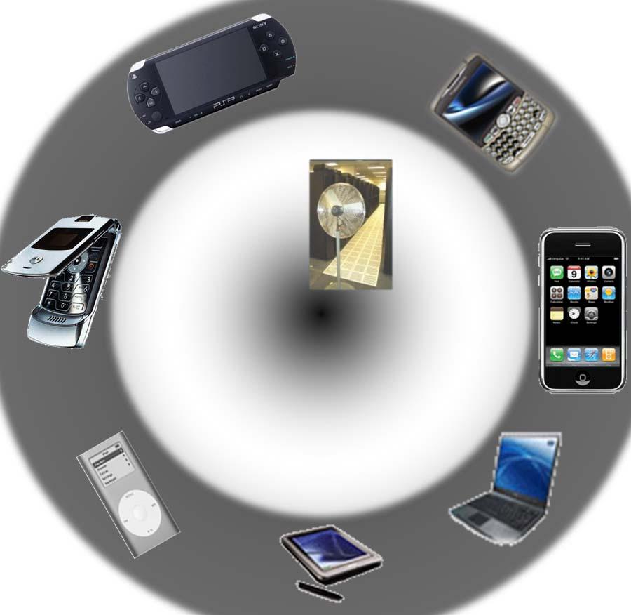


3 Vision for 2020: Swarms of Electronics Infrastructional core Driver for More of Moore s Law Mobile access Driver for More Than Moore s Law Sensory swarm (trillions of devices) J. Rabaey, ASPDAC
4 Why Mechanical Switches? Relays have zero off-state leakage zero leakage energy 3-Terminal Switch Air gap Source t gap Gate Drain t dimple Relays switch on/off abruptly allows for aggressive V DD scaling (ultra-low dynamic energy) Drain Current 1.E-04 1.E-06 1.E-08 1.E-10 1.E-12 1.E-14 Measured I-V S 0.1mV/dec V RL V PI Gate Voltage 4
5 Outline Electro-Mechanical Relay Design for Digital ICs Relay-Based IC Design Relay Reliability Summary


6 4-Terminal Relay Structure Isometric View: Gate Oxide AA cross-section: OFF state Gate Drain A Body Drain Body insulator Source substrate Gate Body A Source AA cross-section: ON state Channel I DS A voltage is applied between the gate and body to bring the channel into contact with the source and drain. Folded-flexure design relieves residual stress. Gate oxide layer insulates the channel from the gate. R. Nathanael et al., IEDM


7 4-T Relay Process Flow (I) Mask 1: Electrode 80 nm Al 2 O 3 50 nm W Si substrate Mask 2: Contact dimple 100nm SiO 2 Mask 3: Channel 50 nm W 100nm 200nm SiO 2 40 nm Al 2 O 3 Deposit Al 2 O 3 substrate insulator ALD at 300 o C Deposit & pattern W electrodes DC magnetron sputtering Deposit 1 st sacrificial LTO LPCVD at 400 o C Define contact regions Deposit 2 nd sacrificial LTO Deposit & pattern W channel Deposit Al 2 O 3 gate oxide R. Nathanael et al., IEDM

8 Mask 4: Structure 4-T Relay Process Flow (II) SiO 2 1 m p+ poly-si 0.4 Ge 0.6 Deposit p+ poly-si 0.4 Ge 0.6 gate LPCVD at 410 o C Pattern gate & gate oxide layers using LTO as a hard mask HF vapor TiO 2 Release in HF vapor Coat with ultra-thin (~0.3nm) TiO 2 ALD at 300 o C R. Nathanael et al., IEDM
 and surface adhesion. R. Nathanael et al., 2009 IEDM / V. Pott et al., Proc. IEEE, Vol. 98, pp.")
9 4-T Relay I D -V G Characteristic Plan View SEM of 4-T Relay 20 μm I DS (A) (a) 1E-02 1E-04 1E-06 1E-08 1E-10 1E-12 1E-14 V B = 9V V B = 0V V D = 2V V S = 0V V GS (V) Zero I OFF ; S < 0.1 mv/dec Hysteresis is due to pull-in mode operation (t dimple > t gap /3) and surface adhesion. R. Nathanael et al., 2009 IEDM / V. Pott et al., Proc. IEEE, Vol. 98, pp ,
 J.")
10 See-Saw Relay Structure Plan View Close-Up of Channel Region Perfectly complementary operation is achieved in left and right channels V BL = 0 V; V BR = 10 V I DS (A) Measured I D -V G Characteristics 1E-03 1E-05 1E-07 1E-09 1E-11 1E-13 I DS_RIGHT V ON_RIGHT =V OFF_LEFT =3.16V I DS_LEFT L A =42μm L A1 =12μm W A =40μm V ON_LEFT =V OFF_RIGHT =7.14V 1E V G (V) J. Jeon et al., IEEE Electron Device Letters, Vol. 31, pp ,
11 See-Saw Relay Latch V WL SRAM Cell V CTRL Storage Node V SN NMOS V BL NMOS V DATA B L GND D L S L G D R S R Seesaw B R V DD V DATA (V) V CTRL (V) V WL (V) V BL (V) Demonstrated SRAM Cell Operation R = READ W = WRITE W '0' V DD =12V W '0' W '1' W '1' R '0' R '0' R '1' R '1' (b-a) (b-b) (b-c) (b-d) Time (s) J. Jeon et al., IEEE/ASME J. MicroElectroMechanical Systems, Vol. 19, pp ,
12 4-T Relay Turn-On Delay Turn-ON Time vs. Gate Voltage Turn-ON Time vs. Body Bias Turn-on delay improves with gate overdrive, and saturates at ~200ns for V B = 0V. Turn-on delay improves w/ body biasing to reduce V PI 100ns turn-on delay R. Nathanael et al., IEDM
13 Relay Scaling, Scaling has similar benefits for relays as for MOSFETs. Pull-in Voltage: V PI Relay Parameter A Scaling Factor Spring constant 1 / Mass 1 / 3 Pull-in voltage 1 / Pull-in delay 1 / Switching energy 1 / 3 k eff Device density 2 Power density 1 0 t 3 gap Pull-in Delay: t PI 65 nm Relay Design Parameter Value Actuation Area nm 2 Actuation Gap Dimple Gap Pull-in voltage Pull-in delay mt k eff dimple t gap V V PI DD 15 nm 10 nm 0.4V - 1V 100ns 10ns V. Pott et al., Proc. IEEE, Vol. 98, pp ,
14 Outline Electro-Mechanical Relay Design for Digital ICs Relay-Based IC Design Relay Reliability Summary
15 Digital IC Design with Relays 4 gate delays 1 mechanical delay CMOS: delay is set by electrical time constant Quadratic delay penalty for stacking devices Buffer & distribute logical/electrical effort over many stages Relays: delay is dominated by mechanical movement Can stack ~100 devices before t elec t mech Implement relay logic as a single complex gate F. Chen et al., ICCAD


16 Relay-Based VLSI Building Blocks 2010 ISSCC Jack Raper Award for Outstanding Technology Directions F. Chen et al., ISSCC


17 Technology Transfer to SEMATECH UC Berkeley: 1 µm litho 1st prototype: 120 µm x 150 µm SEMATECH: 0.25 µm litho Scaled relay: 20 µm x 20 µm 17
18 Energy-Delay Comparison with CMOS CMOS 30-stage FO4 inverter chain: 0 V V dd Output 30-relay chain: V dd 0 V 65 nm technology transition probability=0.01 cap/cmos inverter=0.57ff Input Output Scaled relay technology is projected to provide for >10x energy savings, at clock rates up to ~100MHz V. Pott et al., Proc. IEEE, Vol. 98, pp ,
19 Outline Electro-Mechanical Relay Design for Digital ICs Relay-Based IC Design Relay Reliability Summary
20 Stiction Hysteresis voltage (V PI -V RL ) scales with the pull-in voltage (V PI ) ignoring surface adhesion force Surface adhesion force scales with area of contacting region(s): Extracted from measured V PI,V RL I DS Relay I-V V RL V PI V GB H. Kam et al., 2009 IEDM 20
21 Contact Design for Logic Gates V DD R ON Mechanical Delay t PI ~ ns Electrical Delay t RC < 1 ps C L High R ON (up to ~10 kω) is acceptable To achieve good endurance and reliability: 1. Use hard electrode material Tungsten 2. Apply a surface coating to reduce surface force and current density ALD TiO 2 F. Chen et al., ICCAD
![Contact Stability ON-state Resistance vs. # ON/OFF Cycles Contact resistance [Ω] 1.E+06 1.E+05 1.E+04 1.E+03 1.](/docs-images/86/93655847/images/22-0.jpg "E+02 100k specification L=25 m Measured in ambient 1.E+0 1.E+3 1.E+6 1.E+9 No.")
 Relative distribution (a. i.) Dimple 19nm (b) 0 10 20 Height 30 40(nm) 50 Height (nm) Dimple 19nm 19nm 19nm (d) 0 10 20 30 40 50 Height (nm) H.")
22 Contact Stability ON-state Resistance vs. # ON/OFF Cycles Contact resistance [Ω] 1.E+06 1.E+05 1.E+04 1.E+03 1.E k specification L=25 m Measured in ambient 1.E+0 1.E+3 1.E+6 1.E+9 No. of on/off cycles AFM Measurements Contact (a) Dimple FRESH CONTACT Never tested (c) Contact Dimple AFTER 10 9 cycles Variations are likely due to W oxidation No surface wear is seen after 1 billion ON/OFF cycles 3 μm 3 μm Relative distribution (a. i.) Relative distribution (a. i.) Dimple 19nm (b) Height 30 40(nm) 50 Height (nm) Dimple 19nm 19nm 19nm (d) Height (nm) H. Kam et al., IEDM 2009, R. Nathanael et al., IEDM
23 Relay Endurance Endurance increases exponentially with decreasing V DD, and linearly with decreasing C L Endurance is projected to exceed V H. Kam et al., IEDM


 15 11 8")

")


24 Nanoscale Relay Technology Sub-100 mv operation is possible Zero I OFF enables V DD scaling without increasing leakage power Hysteresis voltage scales with pull-in voltage Node (nm) Actuation Gap (nm) Pull-in Voltage (mv) Release Voltage (mv) * All dimensions scaled with technology node Source2 Drain2 Device Layout Source1 Drain1 Node (nm) Supply Voltage (V) Mechanical Delay (ns) Footprint for two switches = 14 14F 2 L. Hutin et al., to be published 24
 SEM of NVM Array Cross-sectional SEM Current [A] 1E-04 1E-05 1E-06 1E-07 1E-08 1E-09 1E-10 1E-11 1E-12")
 1E-13-1.5-1 -0.5 0 0.5 1 1.5 V BL [V] W. Kwon et al.")
25 Cross-Point Electro-Mechanical NVM Array Electro-mechanical diode cell design: Open circuit in Reset state Diode in Set state (built-in electric-field electrostatic force) SEM of NVM Array Cross-sectional SEM Current [A] 1E-04 1E-05 1E-06 1E-07 1E-08 1E-09 1E-10 1E-11 1E-12 Measured I-V Set state Reset state Smallest cell layout area (4F 2 ); 3-D stackable Low-voltage operation Excellent retention behavior Multiple-time programmable (> 10,000 cycles) 1E V BL [V] W. Kwon et al., to appear in IEEE Electron Device Letters 25
26 Outline Electro-Mechanical Relay Design for Digital ICs Relay-Based IC Design Relay Reliability Summary
27 Summary Mechanical switches have the ideal properties of zero off-state leakage and abrupt turn-on/turn-off. potential for achieving very low E/op (<1 aj) Dimensional scaling is required to achieve low-voltage operation and adequate reliability V DD < 100 mv endurance > cycles Materials optimization can yield further improvements. New circuit and system architectures are needed to fully realize the potential energy-efficiency benefits. device and circuit design co-optimization is key! 27
28 Acknowledgements NEM-Relay Team (current and former) members: Post-docs: Louis Hutin; Hei Kam (now with Intel); Vincent Pott (now with IME, Singapore) Students: Rhesa Nathanael, Jaeseok Jeon (now with Rutgers U.), I-Ru Chen, Yenhao Chen, Jack Yaung, Matt Spencer; Fred Chen and Hossein Fariborzi (MIT); Chengcheng Wang and Kevin Dwan (UCLA) Funding: DARPA/MTO NEMS Program DARPA/MARCO Focus Center Research Program Center for Circuits and Systems Solutions (C2S2) Center for Materials, Structures, and Devices (MSD) NSF Center of Integrated Nanomechanical Systems (COINS) NSF Center for Energy Efficient Electronics Science (E3S) UC Berkeley Micro/Nanofabrication Laboratory 28
29 Frequently Asked Questions 1. Displacement (x) due to gravity? x mg k eff 0.1fm 2. Mechanical shock causing pull-in? requires acceleration > 10 6 g due to small m (10-14 grams) 3. Thermal vibration? 1 2 k 1 2 BT k 2 eff x x 1Å for T = 300K 29
Beyond Transistor Scaling: New Devices for Ultra Low Energy Information Processing
 Beyond Transistor Scaling: New Devices for Ultra Low Energy Information Processing Prof. Tsu Jae King Liu Department of Electrical Engineering and Computer Sciences University of California, Berkeley,
Integrated Circuit Design with Nano-Electro-Mechanical Switches
 Integrated Circuit Design with Nano-Electro-Mechanical Switches Elad Alon 1, Tsu-Jae King Liu 1, Vladimir Stojanovic 2, Dejan Markovic 3 1 University of California, Berkeley 2 Massachusetts Institute of
Electronics Proliferation through Diversification of Solid-State Devices and Materials
 Electronics Proliferation through Diversification of Solid-State Devices and Materials Prof. Tsu-Jae King Liu Department of Electrical Engineering and Computer Sciences University of California, Berkeley,
Sustaining the Si Revolution: From 3D Transistors to 3D Integration
 Sustaining the Si Revolution: From 3D Transistors to 3D Integration Tsu Jae King Liu Department of Electrical Engineering and Computer Sciences University of California, Berkeley, CA USA February 23, 2015
Design of Nano-Electro Mechanical (NEM) Relay Based Nano Transistor for Power Efficient VLSI Circuits
 Relay Based Nano Transistor for Power Efficient VLSI Circuits") Design of Nano-Electro Mechanical (NEM) Relay Based Nano Transistor for Power Efficient VLSI Circuits Arul C 1 and Dr. Omkumar S 2 1 Research Scholar, SCSVMV University, Kancheepuram, India. 2 Associate
Design of Nano-Electro Mechanical (NEM) Relay Based Nano Transistor for Power Efficient VLSI Circuits Arul C 1 and Dr. Omkumar S 2 1 Research Scholar, SCSVMV University, Kancheepuram, India. 2 Associate
FinFET-based Design for Robust Nanoscale SRAM
 FinFET-based Design for Robust Nanoscale SRAM Prof. Tsu-Jae King Liu Dept. of Electrical Engineering and Computer Sciences University of California at Berkeley Acknowledgements Prof. Bora Nikoli Zheng
Lecture #29. Moore s Law
 Lecture #29 ANNOUNCEMENTS HW#15 will be for extra credit Quiz #6 (Thursday 5/8) will include MOSFET C-V No late Projects will be accepted after Thursday 5/8 The last Coffee Hour will be held this Thursday
NW-NEMFET: Steep Subthreshold Nanowire Nanoelectromechanical Field-Effect Transistor
 NW-NEMFET: Steep Subthreshold Nanowire Nanoelectromechanical Field-Effect Transistor Jie Xiang Electrical and Computer Engineering and Materials Science Engineering University of California, San Diego
ECE 5745 Complex Digital ASIC Design Topic 2: CMOS Devices
 ECE 5745 Complex Digital ASIC Design Topic 2: CMOS Devices Christopher Batten School of Electrical and Computer Engineering Cornell University http://www.csl.cornell.edu/courses/ece5950 Simple Transistor
New Devices for Ultra Low Energy Information Processing
 Beyond Transistor Scaling: New Devices for Ultra Low Energy Information Processing Prof. Tsu Jae King Liu Department of Electrical Engineering and Computer Sciences University it of California, i Berkeley,
Advanced Digital Integrated Circuits. Lecture 2: Scaling Trends. Announcements. No office hour next Monday. Extra office hour Tuesday 2-3pm
 EE241 - Spring 20 Advanced Digital Integrated Circuits Lecture 2: Scaling Trends and Features of Modern Technologies Announcements No office hour next Monday Extra office hour Tuesday 2-3pm 2 1 Outline
Fin-Shaped Field Effect Transistor (FinFET) Min Ku Kim 03/07/2018
 Min Ku Kim 03/07/2018") Fin-Shaped Field Effect Transistor (FinFET) Min Ku Kim 03/07/2018 ECE 658 Sp 2018 Semiconductor Materials and Device Characterizations OUTLINE Background FinFET Future Roadmap Keeping up w/ Moore s Law
Fin-Shaped Field Effect Transistor (FinFET) Min Ku Kim 03/07/2018 ECE 658 Sp 2018 Semiconductor Materials and Device Characterizations OUTLINE Background FinFET Future Roadmap Keeping up w/ Moore s Law
Improving CMOS Speed and Switching Energy with Vacuum-Gap Structures
 Improving CMOS Speed and Switching Energy with Vacuum-Gap Structures Chenming Hu and Je Min Park Univ. of California, Berkeley -1- Outline Introduction Background and Motivation MOSFETs with Vacuum-Spacer
Low-Power VLSI. Seong-Ook Jung VLSI SYSTEM LAB, YONSEI University School of Electrical & Electronic Engineering
 Low-Power VLSI Seong-Ook Jung 2013. 5. 27. sjung@yonsei.ac.kr VLSI SYSTEM LAB, YONSEI University School of Electrical & Electronic Engineering Contents 1. Introduction 2. Power classification & Power performance
Micro-Electro-Mechanical Diode for Tunable Power Conversion
 Micro-Electro-Mechanical Diode for Tunable Power Conversion Benjamin Osoba Electrical Engineering and Computer Sciences University of California at Berkeley Technical Report No. UCB/EECS-2016-157 http://www2.eecs.berkeley.edu/pubs/techrpts/2016/eecs-2016-157.html
2009 Spring CS211 Digital Systems & Lab 1 CHAPTER 3: TECHNOLOGY (PART 2)
") 1 CHAPTER 3: IMPLEMENTATION TECHNOLOGY (PART 2) Whatwillwelearninthischapter? we learn in this 2 How transistors operate and form simple switches CMOS logic gates IC technology FPGAs and other PLDs Basic
1 CHAPTER 3: IMPLEMENTATION TECHNOLOGY (PART 2) Whatwillwelearninthischapter? we learn in this 2 How transistors operate and form simple switches CMOS logic gates IC technology FPGAs and other PLDs Basic
Introduction to VLSI ASIC Design and Technology
 Introduction to VLSI ASIC Design and Technology Paulo Moreira CERN - Geneva, Switzerland Paulo Moreira Introduction 1 Outline Introduction Is there a limit? Transistors CMOS building blocks Parasitics
Body-Biased Complementary Logic Implemented Using AlN Piezoelectric MEMS Switches
 University of Pennsylvania From the SelectedWorks of Nipun Sinha 29 Body-Biased Complementary Logic Implemented Using AlN Piezoelectric MEMS Switches Nipun Sinha, University of Pennsylvania Timothy S.
The 3 D Tri Gate transistor is a variant of the FinFET developed at UC Berkeley, and is being used in Intel s 22nmgeneration. microprocessors.
 On May 4, 2011, Intel Corporation announced what it called the most radical shift in semiconductor technology in 50 years. A new 3 dimensional transistor design will enable the production of integrated
III-V CMOS: Quo Vadis?
 III-V CMOS: Quo Vadis? J. A. del Alamo, X. Cai, W. Lu, A. Vardi, and X. Zhao Microsystems Technology Laboratories Massachusetts Institute of Technology Compound Semiconductor Week 2018 Cambridge, MA, May
Logic Synthesis of MEM Relay Circuits
 UNIVERSITY OF CALIFORNIA Los Angeles Logic Synthesis of MEM Relay Circuits A thesis submitted in partial satisfaction of the requirements for the degree Master of Science in Electrical Engineering By Kevin
Metal-Oxide-Silicon (MOS) devices PMOS. n-type
 devices PMOS. n-type") Metal-Oxide-Silicon (MOS devices Principle of MOS Field Effect Transistor transistor operation Metal (poly gate on oxide between source and drain Source and drain implants of opposite type to substrate.
Metal-Oxide-Silicon (MOS devices Principle of MOS Field Effect Transistor transistor operation Metal (poly gate on oxide between source and drain Source and drain implants of opposite type to substrate.
FinFET Devices and Technologies
 FinFET Devices and Technologies Jack C. Lee The University of Texas at Austin NCCAVS PAG Seminar 9/25/14 Material Opportunities for Semiconductors 1 Why FinFETs? Planar MOSFETs cannot scale beyond 22nm
Semiconductor Memory: DRAM and SRAM. Department of Electrical and Computer Engineering, National University of Singapore
 Semiconductor Memory: DRAM and SRAM Outline Introduction Random Access Memory (RAM) DRAM SRAM Non-volatile memory UV EPROM EEPROM Flash memory SONOS memory QD memory Introduction Slow memories Magnetic
Homework 10 posted just for practice. Office hours next week, schedule TBD. HKN review today. Your feedback is important!
 EE141 Fall 2005 Lecture 26 Memory (Cont.) Perspectives Administrative Stuff Homework 10 posted just for practice No need to turn in Office hours next week, schedule TBD. HKN review today. Your feedback
420 Intro to VLSI Design
 Dept of Electrical and Computer Engineering 420 Intro to VLSI Design Lecture 0: Course Introduction and Overview Valencia M. Joyner Spring 2005 Getting Started Syllabus About the Instructor Labs, Problem
Lecture 12 Memory Circuits. Memory Architecture: Decoders. Semiconductor Memory Classification. Array-Structured Memory Architecture RWM NVRWM ROM
 Semiconductor Memory Classification Lecture 12 Memory Circuits RWM NVRWM ROM Peter Cheung Department of Electrical & Electronic Engineering Imperial College London Reading: Weste Ch 8.3.1-8.3.2, Rabaey
Design cycle for MEMS
 Design cycle for MEMS Design cycle for ICs IC Process Selection nmos CMOS BiCMOS ECL for logic for I/O and driver circuit for critical high speed parts of the system The Real Estate of a Wafer MOS Transistor
Low Transistor Variability The Key to Energy Efficient ICs
 Low Transistor Variability The Key to Energy Efficient ICs 2 nd Berkeley Symposium on Energy Efficient Electronic Systems 11/3/11 Robert Rogenmoser, PhD 1 BEES_roro_G_111103 Copyright 2011 SuVolta, Inc.
Sub-30 nm InAs Quantum-Well MOSFETs with Self-Aligned Metal Contacts and Sub-1 nm EOT HfO 2 Insulator
 Sub-30 nm InAs Quantum-Well MOSFETs with Self-Aligned Metal Contacts and Sub-1 nm EOT HfO 2 Insulator Jianqiang Lin, Dimitri A. Antoniadis, and Jesús A. del Alamo Microsystems Technology Laboratories,
III-V CMOS: the key to sub-10 nm electronics?
 III-V CMOS: the key to sub-10 nm electronics? J. A. del Alamo Microsystems Technology Laboratories, MIT 2011 MRS Spring Meeting and Exhibition Symposium P: Interface Engineering for Post-CMOS Emerging
+1 (479)
") Introduction to VLSI Design http://csce.uark.edu +1 (479) 575-6043 yrpeng@uark.edu Invention of the Transistor Vacuum tubes ruled in first half of 20th century Large, expensive, power-hungry, unreliable
Introduction to VLSI Design http://csce.uark.edu +1 (479) 575-6043 yrpeng@uark.edu Invention of the Transistor Vacuum tubes ruled in first half of 20th century Large, expensive, power-hungry, unreliable
100nm Thick Aluminum Nitride Based Piezoelectric Nano Switches Exhibiting 1mV Threshold Voltage Via Body-Biasing
 University of Pennsylvania From the SelectedWorks of Nipun Sinha 2010 100nm Thick Aluminum Nitride Based Piezoelectric Nano Switches Exhibiting 1mV Threshold Voltage Via Body-Biasing Nipun Sinha, University
Practical Information
 EE241 - Spring 2013 Advanced Digital Integrated Circuits MW 2-3:30pm 540A/B Cory Practical Information Instructor: Borivoje Nikolić 509 Cory Hall, 3-9297, bora@eecs Office hours: M 11-12, W 3:30pm-4:30pm
Practical Information
 EE241 - Spring 2010 Advanced Digital Integrated Circuits TuTh 3:30-5pm 293 Cory Practical Information Instructor: Borivoje Nikolić 550B Cory Hall, 3-9297, bora@eecs Office hours: M 10:30am-12pm Reader:
EE 42/100 Lecture 23: CMOS Transistors and Logic Gates. Rev A 4/15/2012 (10:39 AM) Prof. Ali M. Niknejad
 Prof. Ali M. Niknejad") A. M. Niknejad University of California, Berkeley EE 100 / 42 Lecture 23 p. 1/16 EE 42/100 Lecture 23: CMOS Transistors and Logic Gates ELECTRONICS Rev A 4/15/2012 (10:39 AM) Prof. Ali M. Niknejad University
A. M. Niknejad University of California, Berkeley EE 100 / 42 Lecture 23 p. 1/16 EE 42/100 Lecture 23: CMOS Transistors and Logic Gates ELECTRONICS Rev A 4/15/2012 (10:39 AM) Prof. Ali M. Niknejad University
Lecture 0: Introduction
 Lecture 0: Introduction Introduction Integrated circuits: many transistors on one chip. Very Large Scale Integration (VLSI): bucketloads! Complementary Metal Oxide Semiconductor Fast, cheap, low power
VLSI Design. Introduction
 Tassadaq Hussain VLSI Design Introduction Outcome of this course Problem Aims Objectives Outcomes Data Collection Theoretical Model Mathematical Model Validate Development Analysis and Observation Pseudo
ECE520 VLSI Design. Lecture 2: Basic MOS Physics. Payman Zarkesh-Ha
 ECE520 VLSI Design Lecture 2: Basic MOS Physics Payman Zarkesh-Ha Office: ECE Bldg. 230B Office hours: Wednesday 2:00-3:00PM or by appointment E-mail: pzarkesh@unm.edu Slide: 1 Review of Last Lecture Semiconductor
Performance of a Resistance-To-Voltage Read Circuit for Sensing Magnetic Tunnel Junctions
 Performance of a Resistance-To-Voltage Read Circuit for Sensing Magnetic Tunnel Junctions Michael J. Hall Viktor Gruev Roger D. Chamberlain Michael J. Hall, Viktor Gruev, and Roger D. Chamberlain, Performance
Topics. Memory Reliability and Yield Control Logic. John A. Chandy Dept. of Electrical and Computer Engineering University of Connecticut
 Topics Memory Reliability and Yield Control Logic Reliability and Yield Noise Sources in T DRam BL substrate Adjacent BL C WBL α-particles WL leakage C S electrode C cross Transposed-Bitline Architecture
This Week s Subject. DRAM & Flexible RRAM. p-channel MOSFET (PMOS) CMOS: Complementary Metal Oxide Semiconductor
 CMOS: Complementary Metal Oxide Semiconductor") DRAM & Flexible RRAM This Week s Subject p-channel MOSFET (PMOS) CMOS: Complementary Metal Oxide Semiconductor CMOS Logic Inverter NAND gate NOR gate CMOS Integration & Layout GaAs MESFET (JFET) 1 Flexible
DRAM & Flexible RRAM This Week s Subject p-channel MOSFET (PMOS) CMOS: Complementary Metal Oxide Semiconductor CMOS Logic Inverter NAND gate NOR gate CMOS Integration & Layout GaAs MESFET (JFET) 1 Flexible
VLSI Design. Introduction
 VLSI Design Introduction Outline Introduction Silicon, pn-junctions and transistors A Brief History Operation of MOS Transistors CMOS circuits Fabrication steps for CMOS circuits Introduction Integrated
EE4800 CMOS Digital IC Design & Analysis. Lecture 1 Introduction Zhuo Feng
 EE4800 CMOS Digital IC Design & Analysis Lecture 1 Introduction Zhuo Feng 1.1 Prof. Zhuo Feng Office: EERC 730 Phone: 487-3116 Email: zhuofeng@mtu.edu Class Website http://www.ece.mtu.edu/~zhuofeng/ee4800fall2010.html
In pursuit of high-density storage class memory
 Edition October 2017 Semiconductor technology & processing In pursuit of high-density storage class memory A novel thermally stable GeSe-based selector paves the way to storage class memory applications.
Innovation to Advance Moore s Law Requires Core Technology Revolution
 Innovation to Advance Moore s Law Requires Core Technology Revolution Klaus Schuegraf, Ph.D. Chief Technology Officer Silicon Systems Group Applied Materials UC Berkeley Seminar March 9 th, 2012 Innovation
AS THE semiconductor process is scaled down, the thickness
 IEEE TRANSACTIONS ON CIRCUITS AND SYSTEMS II: EXPRESS BRIEFS, VOL. 52, NO. 7, JULY 2005 361 A New Schmitt Trigger Circuit in a 0.13-m 1/2.5-V CMOS Process to Receive 3.3-V Input Signals Shih-Lun Chen,
ISSCC 2006 / SESSION 16 / MEMS AND SENSORS / 16.1
 16.1 A 4.5mW Closed-Loop Σ Micro-Gravity CMOS-SOI Accelerometer Babak Vakili Amini, Reza Abdolvand, Farrokh Ayazi Georgia Institute of Technology, Atlanta, GA Recently, there has been an increasing demand
CMOS VLSI Design (A3425)
") CMOS VLSI Design (A3425) Unit III Static Logic Gates Introduction A static logic gate is one that has a well defined output once the inputs are stabilized and the switching transients have decayed away.
CMOS VLSI Design (A3425) Unit III Static Logic Gates Introduction A static logic gate is one that has a well defined output once the inputs are stabilized and the switching transients have decayed away.
INTERNATIONAL JOURNAL OF APPLIED ENGINEERING RESEARCH, DINDIGUL Volume 1, No 3, 2010
 Low Power CMOS Inverter design at different Technologies Vijay Kumar Sharma 1, Surender Soni 2 1 Department of Electronics & Communication, College of Engineering, Teerthanker Mahaveer University, Moradabad
Design of Optimized Digital Logic Circuits Using FinFET
 Design of Optimized Digital Logic Circuits Using FinFET M. MUTHUSELVI muthuselvi.m93@gmail.com J. MENICK JERLINE jerlin30@gmail.com, R. MARIAAMUTHA maria.amutha@gmail.com I. BLESSING MESHACH DASON blessingmeshach@gmail.com.
Fabrication and Characterization of Emerging Nanoscale Memory
 Fabrication and Characterization of Emerging Nanoscale Memory Yuan Zhang, SangBum Kim, Byoungil Lee, Marissa Caldwell(*), and (*) Chemistry Department Stanford University, Stanford, California, U.S.A.
EECS 427 Lecture 13: Leakage Power Reduction Readings: 6.4.2, CBF Ch.3. EECS 427 F09 Lecture Reminders
 EECS 427 Lecture 13: Leakage Power Reduction Readings: 6.4.2, CBF Ch.3 [Partly adapted from Irwin and Narayanan, and Nikolic] 1 Reminders CAD assignments Please submit CAD5 by tomorrow noon CAD6 is due
Final Exam Topics. IC Technology Advancement. Microelectronics Technology in the 21 st Century. Intel s 90 nm CMOS Technology. 14 nm CMOS Transistors
 ANNOUNCEMENTS Final Exam: When: Wednesday 12/10 12:30-3:30PM Where: 10 Evans (last names beginning A-R) 60 Evans (last names beginning S-Z) Comprehensive coverage of course material Closed book; 3 sheets
Jack Keil Wolf Lecture. ESE 570: Digital Integrated Circuits and VLSI Fundamentals. Lecture Outline. MOSFET N-Type, P-Type.
 ESE 570: Digital Integrated Circuits and VLSI Fundamentals Jack Keil Wolf Lecture Lec 3: January 24, 2019 MOS Fabrication pt. 2: Design Rules and Layout http://www.ese.upenn.edu/about-ese/events/wolf.php
Vertical InAs/GaAsSb/GaSb tunneling field-effect transistor on Si with S = 48 mv/decade and Ion = 10 A/m for Ioff = 1 na/m at VDS = 0.
 Vertical InAs/GaAsSb/GaSb tunneling field-effect transistor on Si with S = 48 mv/decade and Ion = 10 A/m for Ioff = 1 na/m at VDS = 0.3 V Memisevic, E.; Svensson, Johannes; Hellenbrand, Markus; Lind, Erik;
Record I on (0.50 ma/μm at V DD = 0.5 V and I off = 100 na/μm) 25 nm-gate-length ZrO 2 /InAs/InAlAs MOSFETs
 25 nm-gate-length ZrO 2 /InAs/InAlAs MOSFETs") Record I on (0.50 ma/μm at V DD = 0.5 V and I off = 100 na/μm) 25 nm-gate-length ZrO 2 /InAs/InAlAs MOSFETs Sanghoon Lee 1*, V. Chobpattana 2,C.-Y. Huang 1, B. J. Thibeault 1, W. Mitchell 1, S. Stemmer
Record I on (0.50 ma/μm at V DD = 0.5 V and I off = 100 na/μm) 25 nm-gate-length ZrO 2 /InAs/InAlAs MOSFETs Sanghoon Lee 1*, V. Chobpattana 2,C.-Y. Huang 1, B. J. Thibeault 1, W. Mitchell 1, S. Stemmer
Comparison of 32nm High-k Metal Gate Predictive Technology Model CMOS and MOSFET-Like CNFET compact Model Based Domino logic Circuits
 Comparison of 32nm High-k Metal Gate Predictive Technology Model CMOS and MOSFET-Like CNFET compact Model Based Domino logic Circuits Saravana Maruthamuthu, Wireless Group Infineon Technologies India Private
Analysis of Low Power-High Speed Sense Amplifier in Submicron Technology
 Voltage IJSRD - International Journal for Scientific Research & Development Vol. 2, Issue 02, 2014 ISSN (online): 2321-0613 Analysis of Low Power-High Speed Sense Amplifier in Submicron Technology Sunil
Session 10: Solid State Physics MOSFET
 Session 10: Solid State Physics MOSFET 1 Outline A B C D E F G H I J 2 MOSCap MOSFET Metal-Oxide-Semiconductor Field-Effect Transistor: Al (metal) SiO2 (oxide) High k ~0.1 ~5 A SiO2 A n+ n+ p-type Si (bulk)
Nanoscale III-V CMOS
 Nanoscale III-V CMOS J. A. del Alamo Microsystems Technology Laboratories Massachusetts Institute of Technology SEMI Advanced Semiconductor Manufacturing Conference Saratoga Springs, NY; May 16-19, 2016
Depletion-mode operation ( 공핍형 ): Using an input gate voltage to effectively decrease the channel size of an FET
: Using an input gate voltage to effectively decrease the channel size of an FET") Ch. 13 MOSFET Metal-Oxide-Semiconductor Field-Effect Transistor : I D D-mode E-mode V g The gate oxide is made of dielectric SiO 2 with e = 3.9 Depletion-mode operation ( 공핍형 ): Using an input gate voltage
Ch. 13 MOSFET Metal-Oxide-Semiconductor Field-Effect Transistor : I D D-mode E-mode V g The gate oxide is made of dielectric SiO 2 with e = 3.9 Depletion-mode operation ( 공핍형 ): Using an input gate voltage
Wafer-scale 3D integration of silicon-on-insulator RF amplifiers
 Wafer-scale integration of silicon-on-insulator RF amplifiers The MIT Faculty has made this article openly available. Please share how this access benefits you. Your story matters. Citation As Published
ESE 570: Digital Integrated Circuits and VLSI Fundamentals
 ESE 570: Digital Integrated Circuits and VLSI Fundamentals Lec 3: January 24, 2019 MOS Fabrication pt. 2: Design Rules and Layout Penn ESE 570 Spring 2019 Khanna Jack Keil Wolf Lecture http://www.ese.upenn.edu/about-ese/events/wolf.php
Silicon Single-Electron Devices for Logic Applications
 ESSDERC 02/9/25 Silicon Single-Electron Devices for Logic Applications NTT Basic Research Laboratories Yasuo Takahashi Collaborators: : Yukinori Ono, Akira Fujiwara, Hiroshi Inokawa, Kenji Shiraishi, Masao
Announcements. Advanced Digital Integrated Circuits. Quiz #3 today Homework #4 posted This lecture until 4pm
 EE241 - Spring 2011 dvanced Digital Integrated Circuits Lecture 20: High-Performance Logic Styles nnouncements Quiz #3 today Homework #4 posted This lecture until 4pm Reading: Chapter 8 in the owhill text
Static Random Access Memory - SRAM Dr. Lynn Fuller Webpage:
 ROCHESTER INSTITUTE OF TECHNOLOGY MICROELECTRONIC ENGINEERING Static Random Access Memory - SRAM Dr. Lynn Fuller Webpage: http://people.rit.edu/lffeee 82 Lomb Memorial Drive Rochester, NY 14623-5604 Email:
The Design of SET-CMOS Hybrid Logic Style of 1-Bit Comparator
 The Design of SET-CMOS Hybrid Logic Style of 1-Bit Comparator A. T. Fathima Thuslim Department of Electronics and communication Engineering St. Peters University, Avadi, Chennai, India Abstract: Single
Atomic-layer deposition of ultrathin gate dielectrics and Si new functional devices
 Atomic-layer deposition of ultrathin gate dielectrics and Si new functional devices Anri Nakajima Research Center for Nanodevices and Systems, Hiroshima University 1-4-2 Kagamiyama, Higashi-Hiroshima,
Combinational Logic Gates in CMOS
 Combinational Logic Gates in CMOS References: dapted from: Digital Integrated Circuits: Design Perspective, J. Rabaey UC Principles of CMOS VLSI Design: Systems Perspective, 2nd Ed., N. H. E. Weste and
Ultra Low Voltage Operation with Bootstrap Scheme for Single Power Supply SOI-SRAM
 [ 2007 International Conference on VLSI Design ] Jan. 9, 2007 Ultra Low Voltage Operation with Bootstrap Scheme for Single Power Supply SOI-SRAM Masaaki Iijima, Masayuki Kitamura, Masahiro Numa, *Akira
Low Energy Communication: NanoPhotonic & Electrical. Prof. Eli Yablonovitch EECS Dept. UC Berkeley
 Low Energy Communication: NanoPhotonic & Electrical Prof. Eli Yablonovitch EECS Dept. UC Berkeley What is the energy cost of reading out your flash memory? Read the current going through a resistor, in
IR2110 HIGH AND LOW SIDE DRIVER. Features. Product Summary. Packages. Description. Typical Connection. 500V max. V OFFSET 10-20V VOUT.
 Features n Floating channel designed for bootstrap operation Fully operational to +5V Tolerant to negative transient voltage dv/dt immune n Gate drive supply range from 1 to 2V n Undervoltage lockout for
Chapter 4. CMOS Cascode Amplifiers. 4.1 Introduction. 4.2 CMOS Cascode Amplifiers
 Chapter 4 CMOS Cascode Amplifiers 4.1 Introduction A single stage CMOS amplifier cannot give desired dc voltage gain, output resistance and transconductance. The voltage gain can be made to attain higher
A novel high performance 3 VDD-tolerant ESD detection circuit in advanced CMOS process
 LETTER IEICE Electronics Express, Vol.14, No.21, 1 10 A novel high performance 3 VDD-tolerant ESD detection circuit in advanced CMOS process Xiaoyun Li, Houpeng Chen a), Yu Lei b), Qian Wang, Xi Li, Jie
problem grade total
 Fall 2005 6.012 Microelectronic Devices and Circuits Prof. J. A. del Alamo Name: Recitation: November 16, 2005 Quiz #2 problem grade 1 2 3 4 total General guidelines (please read carefully before starting):
Low Power High Performance 10T Full Adder for Low Voltage CMOS Technology Using Dual Threshold Voltage
 Low Power High Performance 10T Full Adder for Low Voltage CMOS Technology Using Dual Threshold Voltage Surbhi Kushwah 1, Shipra Mishra 2 1 M.Tech. VLSI Design, NITM College Gwalior M.P. India 474001 2
Topic 3. CMOS Fabrication Process
 Topic 3 CMOS Fabrication Process Peter Cheung Department of Electrical & Electronic Engineering Imperial College London URL: www.ee.ic.ac.uk/pcheung/ E-mail: p.cheung@ic.ac.uk Lecture 3-1 Layout of a Inverter
Total reduction of leakage power through combined effect of Sleep stack and variable body biasing technique
 Total reduction of leakage power through combined effect of Sleep and variable body biasing technique Anjana R 1, Ajay kumar somkuwar 2 Abstract Leakage power consumption has become a major concern for
45nm Bulk CMOS Within-Die Variations. Courtesy of C. Spanos (UC Berkeley) Lecture 11. Process-induced Variability I: Random
 Lecture 11. Process-induced Variability I: Random") 45nm Bulk CMOS Within-Die Variations. Courtesy of C. Spanos (UC Berkeley) Lecture 11 Process-induced Variability I: Random Random Variability Sources and Characterization Comparisons of Different MOSFET
45nm Bulk CMOS Within-Die Variations. Courtesy of C. Spanos (UC Berkeley) Lecture 11 Process-induced Variability I: Random Random Variability Sources and Characterization Comparisons of Different MOSFET
Semiconductor Physics and Devices
 Metal-Semiconductor and Semiconductor Heterojunctions The Metal-Oxide-Semiconductor Field-Effect Transistor (MOSFET) is one of two major types of transistors. The MOSFET is used in digital circuit, because
ECE 340 Lecture 37 : Metal- Insulator-Semiconductor FET Class Outline:
 ECE 340 Lecture 37 : Metal- Insulator-Semiconductor FET Class Outline: Metal-Semiconductor Junctions MOSFET Basic Operation MOS Capacitor Things you should know when you leave Key Questions What is the
InGaAs MOSFETs for CMOS:
 InGaAs MOSFETs for CMOS: Recent Advances in Process Technology J. A. del Alamo, D. Antoniadis, A. Guo, D.-H. Kim 1, T.-W. Kim 2, J. Lin, W. Lu, A. Vardi and X. Zhao Microsystems Technology Laboratories,
LSI ON GLASS SUBSTRATES
 LSI ON GLASS SUBSTRATES OUTLINE Introduction: Why System on Glass? MOSFET Technology Low-Temperature Poly-Si TFT Technology System-on-Glass Technology Issues Conclusion System on Glass CPU SRAM DRAM EEPROM
Sub-Threshold Region Behavior of Long Channel MOSFET
 Sub-threshold Region - So far, we have discussed the MOSFET behavior in linear region and saturation region - Sub-threshold region is refer to region where Vt is less than Vt - Sub-threshold region reflects
ESD-Transient Detection Circuit with Equivalent Capacitance-Coupling Detection Mechanism and High Efficiency of Layout Area in a 65nm CMOS Technology
 ESD-Transient Detection Circuit with Equivalent Capacitance-Coupling Detection Mechanism and High Efficiency of Layout Area in a 65nm CMOS Technology Chih-Ting Yeh (1, 2) and Ming-Dou Ker (1, 3) (1) Department
Energy Efficiency of Power-Gating in Low-Power Clocked Storage Elements
 Energy Efficiency of Power-Gating in Low-Power Clocked Storage Elements Christophe Giacomotto 1, Mandeep Singh 1, Milena Vratonjic 1, Vojin G. Oklobdzija 1 1 Advanced Computer systems Engineering Laboratory,
IFSIN. WEB PAGE Fall ://weble.upc.es/ifsin/
 IFSIN IMPLEMENTACIÓ FÍSICA DE SISTEMES INTEGRATS NANOMÈTRICS IMPLEMENTACIÓN N FÍSICA F DE SISTEMAS INTEGRADOS NANOMÉTRICOS PHYSICAL IMPLEMENTATION OF NANOMETER INTEGRATED SYSTEMS Fall 2008 Prof. Xavier
InAs Quantum-Well MOSFET for logic and microwave applications
 AWAD June 29 th 2012 Accelerating the next technology revolution InAs Quantum-Well MOSFET for logic and microwave applications T.-W. Kim, R. Hill, C. D. Young, D. Veksler, L. Morassi, S. Oktybrshky 1,
MOSFET & IC Basics - GATE Problems (Part - I)
") MOSFET & IC Basics - GATE Problems (Part - I) 1. Channel current is reduced on application of a more positive voltage to the GATE of the depletion mode n channel MOSFET. (True/False) [GATE 1994: 1 Mark]
MOSFET & IC Basics - GATE Problems (Part - I) 1. Channel current is reduced on application of a more positive voltage to the GATE of the depletion mode n channel MOSFET. (True/False) [GATE 1994: 1 Mark]
Sleepy Keeper Approach for Power Performance Tuning in VLSI Design
 International Journal of Electronics and Communication Engineering. ISSN 0974-2166 Volume 6, Number 1 (2013), pp. 17-28 International Research Publication House http://www.irphouse.com Sleepy Keeper Approach
PERFORMANCE CHARACTERISTICS OF EPAD PRECISION MATCHED PAIR MOSFET ARRAY
 TM ADVANCED LINEAR DEVICES, INC. e EPAD E N A B L E D PERFORMANCE CHARACTERISTICS OF EPAD PRECISION MATCHED PAIR MOSFET ARRAY GENERAL DESCRIPTION ALDxx/ALD9xx/ALDxx/ALD9xx are high precision monolithic
Gigahertz Ambipolar Frequency Multiplier Based on Cvd Graphene
 Gigahertz Ambipolar Frequency Multiplier Based on Cvd Graphene The MIT Faculty has made this article openly available. Please share how this access benefits you. Your story matters. Citation As Published
CMPEN 411 VLSI Digital Circuits Spring Lecture 24: Peripheral Memory Circuits
 CMPEN 411 VLSI Digital Circuits Spring 2011 Lecture 24: Peripheral Memory Circuits [Adapted from Rabaey s Digital Integrated Circuits, Second Edition, 2003 J. Rabaey, A. Chandrakasan, B. Nikolic] Sp11
Towards Sub-10 nm Diameter InGaAs Vertical nanowire MOSFETs and TFETs
 Towards Sub-10 nm Diameter InGaAs Vertical nanowire MOSFETs and TFETs J. A. del Alamo, X. Zhao, W. Lu, and A. Vardi Microsystems Technology Laboratories Massachusetts Institute of Technology 5 th Berkeley
I DDQ Current Testing
 I DDQ Current Testing Motivation Early 99 s Fabrication Line had 5 to defects per million (dpm) chips IBM wanted to get 3.4 defects per million (dpm) chips Conventional way to reduce defects: Increasing
Architecture of Computers and Parallel Systems Part 9: Digital Circuits
 Architecture of Computers and Parallel Systems Part 9: Digital Circuits Ing. Petr Olivka petr.olivka@vsb.cz Department of Computer Science FEI VSB-TUO Architecture of Computers and Parallel Systems Part
Low Power Design of Schmitt Trigger Based SRAM Cell Using NBTI Technique
 Low Power Design of Schmitt Trigger Based SRAM Cell Using NBTI Technique M.Padmaja 1, N.V.Maheswara Rao 2 Post Graduate Scholar, Gayatri Vidya Parishad College of Engineering for Women, Affiliated to JNTU,
EECS130 Integrated Circuit Devices
 EECS130 Integrated Circuit Devices Professor Ali Javey 11/6/2007 MOSFETs Lecture 6 BJTs- Lecture 1 Reading Assignment: Chapter 10 More Scalable Device Structures Vertical Scaling is important. For example,
Analyzing Combined Impacts of Parameter Variations and BTI in Nano-scale Logical Gates
 Analyzing Combined Impacts of Parameter Variations and BTI in Nano-scale Logical Gates Seyab Khan Said Hamdioui Abstract Bias Temperature Instability (BTI) and parameter variations are threats to reliability