Static Random Access Memory - SRAM Dr. Lynn Fuller Webpage:
|
|
|
- Gladys Houston
- 6 years ago
- Views:
Transcription
1 ROCHESTER INSTITUTE OF TECHNOLOGY MICROELECTRONIC ENGINEERING Static Random Access Memory - SRAM Dr. Lynn Fuller Webpage: 82 Lomb Memorial Drive Rochester, NY Lynn.Fuller@rit.edu Department webpage: SRAM.ppt Page 1
2 ADOBE PRESENTER This PowerPoint module has been published using Adobe Presenter. Please click on the Notes tab in the left panel to read the instructors comments for each slide. Manually advance the slide by clicking on the play arrow or pressing the page down key. Page 2
3 OUTLINE Introduction Memory Organization Bitline Capacitance Column Pullups Column Select Write/Read Operation Write/Read Circuitry Sense Amplifiers References Homework Page 3
4 INTRODUCTION Read-Only Memories (ROMs) - These are used to store information that will not change during the life of the system. They are permanently programmed during manufacture. Nonvolatile read-write Memories (EPROM, EEPROM) - These devices retain the information stored in them when the power is turned off. They can be erased but usually much slower than they can be written. The number of erase/write cycles may be limited. Dynamic Random Access Memories (DRAMs) - Information is stored as charge on a capacitor. The stored charge will eventually leak away so DRAMs must be periodically refreshed. Typically DRAMs are refreshed every 5-50 milli seconds. One transistor one capacitor per cell. Static Random Access Memories (SRAM) - These devices store information in two cross-coupled inverters. Such a memory does not need to be refreshed. CMOS SRAM is low power. The SRAM cell requires six transistors making it fewer bits per chip than DRAM. Page 4

5 INTRODUCTION NAND Flash has smallest unit cell, then DRAM and SRAM. Page 5
6 SRAM CELL LAYOUT SIZE Cell Layout size has been shrinking as technology improves Page 6

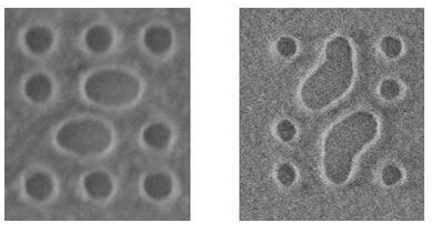
7 B BB SRAM SEM OF SRAM SHOWING UNIT CELL Wordline 0.65µm x 0.25µm = 0.16um 2 M5 Q M3 M4 Q M6 M1 M2 BB T5 T1 VSS OFF T3 These pictures show transistor gates and active regions. The metal interconnect is above the transistors and is not shown. VSS T4 T2 T6 BL Page 7
8 FINFET SRAM REDUCES CELL SIZE Page 8
9 Bit Line Bit Line MEMORY ORGANIZATION The peripheral circuits include multiplexers, decoders, sense amplifiers, column precharge, data buffers, Read-Write circuits, and more. These circuits have to work for millions of storage locations. Precharge Electronics Word line Word line Read/Write R/W Control Sense Enable Write Enable Decoder Word line Read/Write Column Decoder Column MUX Sense Amplifiers Page 9
10 B-1 Bitline-1 SRAM Bitline-1 BB-1 B-2 Bitline-2 Bitline-2 BB-2 6 TRANSISTOR SRAM CELL -1 Wordline-1 Q Q Q Q -2 Wordline-2 Page 10
11 B BB B BB B BB COLUMN PULLUPS In both read and write operations both bitlines are pulled up to near. The circuits used to precharge the bitlines depends on the type of sensing that is used in the read operation. Shown here are three different pullup circuits. A balance transistor between both bitlines ensures that both bitlines are at the same voltage after precharge. Once the precharge is completed the word lines goes high and one of the bitlines remains high while the other goes low. The millivolt difference is amplified by the sense amplifier. Current sense amplifiers require transistors that are always on as show in the two circuits on the right. Precharge Electronics PC PC PC Page 11
12 BITLINE AND WORDLINE CAPACITANCE Using the following parameters we will estimate the capacitance of the word and bitlines. Assume we have a 16Kbit memory organized as 2048 words each of 8-bits. The wiring capacitance is 0.2fF/um of length. Assuming a length of 1mm we add 200fF for each Bitline and only 3.3fF for each Wordline. (these wordlines are only 8 cells long) (note: selected memory organization will change resutlts significantly) The two pass transistors in each cell that are connected to the wordline have W/L = 0.5um/0.1um for an area of 0.05um2 and using 50Å gate oxide thickness results in a capacitance of 0.345fF/transistor and 0.69fF/cell. For an 8-Bit word the wordline capacitance is 8 times 0.69fF plus the wiring capacitance which is 3.3fF for a total of 8.8fF Wordline Capacitance = 8.8fF 350nm W = 500nm 2l 2l 2l l L = 2l = 100nm Page 12
13 BITLINE AND WORDLINE CAPACITANCE Wordline Capacitance = 8.8fF (from previous page) The bitlines are connected to the drain/source of one transistor per cell. In 100nm technology this results in transistor D/S area of 0.5um x 0.35um= 0.175um 2 and perimeter of ~1.7um. With doping levels ~3E17cm-3 the width of the space charge layer is 0.08um giving junction capacitance of 0.45fF/cell. For 2048 cells connected to the bitline the total capacitance per bitline is 0.922pF plus the wiring capacitance of 200fF for a total of 1.1pF. Bitline Capacitance = 1.1pF 350nm W = 500nm 2l 2l 2l l L = 2l = 100nm Page 13
14 B BB READ OPERATION 0 0 PC t t M5 M3 M4 M6 0 0 B, BB Q QB t t Cbit Q M1 M2 QB Cbit Cbit represents the Bit Line Capacitance Page 14
15 READ OPERATION The precharge raises the bitline to near volts. Once the wordline, is activated the bitlines are connected to the crosscoupled inverter storage cell through a pass transistor. If Q is high QB is low and vise versa. The bitline connected to the low side of the cell inverters will begin to discharge through the pass transistor and the NMOS transistor in the inverter to ground. The voltage on that bitline will decrease slowly while the other bitline will remain high. Once the voltage difference reaches a couple hundred millivolts the amplifier is saturated and the value is stored in a data latch. The wordline is set to zero and the bitlines are recharged high. The cell resets itself to its original state. The transistor sizes for read stability should be such that it does not disturb the original state stored in the cell. The current flows from the bitline through the pass transistor and the NMOS transistor in the inverter. If the NMOS has 3 or 4 times the conductance of the PMOS transistor in that inverter the voltage will remain close enough to low to not disturb the stored value. Page 15
16 B BB READ CIRCUITRY clk PC pc addr data M7 M9 M8 B, BB Cbit M5 Q M3 M4 QB M6 Cbit QB Q COL sense M10 M1 M2 Write Driver M11 Data out SENSE ENABLE SENSE AMPLIFIER OUT Page 16
17 READ CIRCUITRY The precharge raises the bitline to near volts. Once the wordline,, is activated the SRAM cell attempts to drive the bitlines to high or low as appropriate. The large capacitance of the bitlines would require a long time to charge or discharge. However the sense amplifier needs only a few 100 s of millivolt difference between B and BB to amplify to obtain the appropriate output voltage. The time required is relatively short. The is returned to its standby state and the cross coupled inverters return the Q and QB nodes to the appropriate voltages representing the stored data. Page 17
18 BL Bitline-1 SRAM Bitline-1 BB DIFFERENTIAL VOLTAGE SENSE AMPLIFIER Output Bias Page 18
19 Bit Line Bit Line SRAM COLUMN SELECTION Precharge Electronics Row Decoder Column Decoder Column MUX Sense Amplifiers Write Enable Sense Enable R/W Control R/W Page 19
20 ANALOG SWITCHES TRANSMISSION GATE I PMOS Vt= -1 S zero D C V1 V2 V1 V2 D NMOS Vt=+1 +5 S C Transmission Gate For current flowing to the right (ie V1>V2) the PMOS transistor will be on if V1 is greater than the threshold voltage, the NMOS transistor will be on if V2 is <4 volts. If we are charging up a capacitor load at node 2, to 5 volts, initially current will flow through NMOS and PMOS but once V2 gets above 4 volts the NMOS will be off. If we are trying to charge up V2 to V1 = +1 volt the PMOS will never be on. A complementary situation occurs for current flow to the left. Single transistor switches can be used if we are sure the Vgs will be more than the threshold voltage for the specific circuit application. (or use larger voltages on the gates) Page 20
21 B BB WRITE OPERATION The operation of writing 0 or 1 is done by forcing one of the bitlines low while leaving the other high. The pass transistors must be wider (~2x) than the PMOS transistors in the inverters to be able to overpower the cell and pull the inverter output low enough to initiate a regenerative effect between the two inverters. Once the inverters have reached their new written state the wordline can be returned to its standby state (low). OFF M5 Q Wordline For example if Q is 0 and you want to write a 1 then BB is connected to GND while B is left floating (high after precharge). The wordline turns on M5 and M6 and the output Q goes low and eventually Q goes high. M3 M4 M1 M2 Q M6 Page 21
22 B BB WRITE CIRCUITRY clk PC pc M7 M9 M8 addr data Cbit M5 Q M3 M4 QB M6 Cbit COL B, BB QB Q W D M1 M2 M13 Write Driver COL SELECT M15 M14 W D Page 22
23 WRITE CIRCUITRY First the columns are precharged to using M7, M8 and M9. Next, the address and data signals are set up and held stable and then the clock is applied. The address signals are converted into colum select and wordline activation signals. The data and write signals are applied and then the wordline is enabled. Only one of the two bitlines will be connected to GND, the other remains high from the precharge operation. M13, M14 and M15 are sized to pull down the bitline in a specified time. Once the cell is written the wordline and column select lines return to their standby value. Page 23
24 SRAM CELL WITH PC, READ AND WRITE CIRCUITRY PC R V DD = 1.2 V PC M 7 M 8 20l/2l M 11 V DD = 1.2 V 2l/2l 20l/2l PC R C bit = 1 pf M 5 M 6 10 ff 10 ff C bit = 1 pf BL 4l/2l M 3 Q 10l/2l _ Q M 1 M 2 10l/2l M 4 4l/2l BL WE _ D M 9 M 10 WE D Page 24

25 SPICE FOR SRAM WRITE This is a schematic of the sense amplifier and waveforms for the SRAM Rochester Institute Write of Technology operation. L/W for Pass=2/8, NMOS=2/16, PMOS=2/4 Page 25
26 SPICE FOR SRAM WRITE ONE Waveforms for the SRAM Write 1 operation. Page 26
27 SPICE FOR SRAM WRITE ZERO Waveforms for the SRAM Write 0 operation. Page 27

28 SPICE FOR SRAM READ This is a schematic of the sense amplifier and waveforms for the SRAM Rochester Institute Read of Technology operation. L/W for Pass=2/8, NMOS=2/16, PMOS=2/4 Page 28
29 SPICE FOR SRAM READ Waveforms for the SRAM READ operation. Page 29
30 SRAM LAYOUT SHOWING TWO LAYERS METAL BB BL VSS pmos pmos Active Poly CC Metal 1 Via Metal 2 BL VSS Page 30
31 SRAM LAYOUT SHOWING TWO LAYERS METAL Note: PMOS W>NMOS W L s different for PMOS BB BL VSS Cell layout can be copied and pasted to make array pmos pmos BL VSS Page 31
32 SRAM LAYOUT ARRAY BB BL VSS BB BL VSS pmos pmos pmos pmos BB BL BL VSS VSS BB BL BL VSS VSS pmos pmos pmos pmos Rochester Institute of Technology VSS BL VSS BL Page 32
33 FINFET SRAM REDUCES CELL SIZE Page 33

34 SEM OF SRAM CELL USING FINFETS These pictures show transistor gates and active regions. The metal interconnect is above the transistors and is not shown. 0.47µm x 0.2µm = 0.094um 2 Page 34

35 LAYOUT AFFECTS LITHOGRAPHY Page 35

36 REFERNCES 1. Hodges Jackson and Saleh, Analysis and Design of Digital Integrated Circuits, Chapter Sedra and Smith, Microelectronic Circuits, Sixth Edition, Chapter Dr. Fuller s Lecture Notes, Page 36
37 HOMEWORK SRAM 1. Use SPICE to illustrate the operation of the SRAM cell. Show write of 0 and 1, show read. 2. Investigate the speed of operation of the SRAM cell using SPICE. 3. Design the sense amplifier and a data latch to read the cell. Page 37

38 HOMEWORK SRAM SRAM cell plus sense amplifier and data latch. Zach Allen, 2016 Page 38

39 HOMEWORK SRAM SRAM cell plus sense amplifier and data latch. Zach Allen, 2016 Page 39
Memory Basics. historically defined as memory array with individual bit access refers to memory with both Read and Write capabilities
 Memory Basics RAM: Random Access Memory historically defined as memory array with individual bit access refers to memory with both Read and Write capabilities ROM: Read Only Memory no capabilities for
Lecture 12 Memory Circuits. Memory Architecture: Decoders. Semiconductor Memory Classification. Array-Structured Memory Architecture RWM NVRWM ROM
 Semiconductor Memory Classification Lecture 12 Memory Circuits RWM NVRWM ROM Peter Cheung Department of Electrical & Electronic Engineering Imperial College London Reading: Weste Ch 8.3.1-8.3.2, Rabaey
Electronic Circuits EE359A
 Electronic Circuits EE359A Bruce McNair B206 bmcnair@stevens.edu 201-216-5549 1 Memory and Advanced Digital Circuits - 2 Chapter 11 2 Figure 11.1 (a) Basic latch. (b) The latch with the feedback loop opened.
CMPEN 411 VLSI Digital Circuits Spring Lecture 24: Peripheral Memory Circuits
 CMPEN 411 VLSI Digital Circuits Spring 2011 Lecture 24: Peripheral Memory Circuits [Adapted from Rabaey s Digital Integrated Circuits, Second Edition, 2003 J. Rabaey, A. Chandrakasan, B. Nikolic] Sp11
Memory (Part 1) RAM memory
 RAM memory") Budapest University of Technology and Economics Department of Electron Devices Technology of IT Devices Lecture 7 Memory (Part 1) RAM memory Semiconductor memory Memory Overview MOS transistor recap and
Budapest University of Technology and Economics Department of Electron Devices Technology of IT Devices Lecture 7 Memory (Part 1) RAM memory Semiconductor memory Memory Overview MOS transistor recap and
電子電路. Memory and Advanced Digital Circuits
 電子電路 Memory and Advanced Digital Circuits Hsun-Hsiang Chen ( 陳勛祥 ) Department of Electronic Engineering National Changhua University of Education Email: chenhh@cc.ncue.edu.tw Spring 2010 2 Reference Microelectronic
EEC 118 Lecture #12: Dynamic Logic
 EEC 118 Lecture #12: Dynamic Logic Rajeevan Amirtharajah University of California, Davis Jeff Parkhurst Intel Corporation Outline Today: Alternative MOS Logic Styles Dynamic MOS Logic Circuits: Rabaey
DESIGN & IMPLEMENTATION OF SELF TIME DUMMY REPLICA TECHNIQUE IN 128X128 LOW VOLTAGE SRAM
 DESIGN & IMPLEMENTATION OF SELF TIME DUMMY REPLICA TECHNIQUE IN 128X128 LOW VOLTAGE SRAM 1 Mitali Agarwal, 2 Taru Tevatia 1 Research Scholar, 2 Associate Professor 1 Department of Electronics & Communication
Homework 10 posted just for practice. Office hours next week, schedule TBD. HKN review today. Your feedback is important!
 EE141 Fall 2005 Lecture 26 Memory (Cont.) Perspectives Administrative Stuff Homework 10 posted just for practice No need to turn in Office hours next week, schedule TBD. HKN review today. Your feedback
EE 42/100 Lecture 23: CMOS Transistors and Logic Gates. Rev A 4/15/2012 (10:39 AM) Prof. Ali M. Niknejad
 Prof. Ali M. Niknejad") A. M. Niknejad University of California, Berkeley EE 100 / 42 Lecture 23 p. 1/16 EE 42/100 Lecture 23: CMOS Transistors and Logic Gates ELECTRONICS Rev A 4/15/2012 (10:39 AM) Prof. Ali M. Niknejad University
A. M. Niknejad University of California, Berkeley EE 100 / 42 Lecture 23 p. 1/16 EE 42/100 Lecture 23: CMOS Transistors and Logic Gates ELECTRONICS Rev A 4/15/2012 (10:39 AM) Prof. Ali M. Niknejad University
Lecture #29. Moore s Law
 Lecture #29 ANNOUNCEMENTS HW#15 will be for extra credit Quiz #6 (Thursday 5/8) will include MOSFET C-V No late Projects will be accepted after Thursday 5/8 The last Coffee Hour will be held this Thursday
A Robust Low Power Static Random Access Memory Cell Design
 Wright State University CORE Scholar Browse all Theses and Dissertations Theses and Dissertations 2018 A Robust Low Power Static Random Access Memory Cell Design A. V. Rama Raju Pusapati Wright State University
Lecture 6: Electronics Beyond the Logic Switches Xufeng Kou School of Information Science and Technology ShanghaiTech University
 Lecture 6: Electronics Beyond the Logic Switches Xufeng Kou School of Information Science and Technology ShanghaiTech University EE 224 Solid State Electronics II Lecture 3: Lattice and symmetry 1 Outline
Semiconductor Memory: DRAM and SRAM. Department of Electrical and Computer Engineering, National University of Singapore
 Semiconductor Memory: DRAM and SRAM Outline Introduction Random Access Memory (RAM) DRAM SRAM Non-volatile memory UV EPROM EEPROM Flash memory SONOS memory QD memory Introduction Slow memories Magnetic
Preface to Third Edition Deep Submicron Digital IC Design p. 1 Introduction p. 1 Brief History of IC Industry p. 3 Review of Digital Logic Gate
 Preface to Third Edition p. xiii Deep Submicron Digital IC Design p. 1 Introduction p. 1 Brief History of IC Industry p. 3 Review of Digital Logic Gate Design p. 6 Basic Logic Functions p. 6 Implementation
Device Technologies. Yau - 1
 Device Technologies Yau - 1 Objectives After studying the material in this chapter, you will be able to: 1. Identify differences between analog and digital devices and passive and active components. Explain
MOS Inverters Dr. Lynn Fuller Webpage:
 ROCHESTER INSTITUTE OF TECHNOLOGY MICROELECTRONIC ENGINEERING MOS Inverters Webpage: http://people.rit.edu/lffeee 82 Lomb Memorial Drive Rochester, NY 14623-5604 Tel (585) 475-2035 Email: Lynn.Fuller@rit.edu
Design of a high speed and low power Sense Amplifier
 Design of a high speed and low power Sense Amplifier A dissertation submitted in partial fulfillment of the requirement for the award of degree of Master of Technology in VLSI Design & CAD Submitted by
A Low-Power SRAM Design Using Quiet-Bitline Architecture
 A Low-Power SRAM Design Using uiet-bitline Architecture Shin-Pao Cheng Shi-Yu Huang Electrical Engineering Department National Tsing-Hua University, Taiwan Abstract This paper presents a low-power SRAM
! Sequential Logic. ! Timing Hazards. ! Dynamic Logic. ! Add state elements (registers, latches) ! Compute. " From state elements
 ! Compute. From state elements") ESE 570: Digital Integrated Circuits and VLSI Fundamentals Lec 19: April 2, 2019 Sequential Logic, Timing Hazards and Dynamic Logic Lecture Outline! Sequential Logic! Timing Hazards! Dynamic Logic 4 Sequential
ESE 570: Digital Integrated Circuits and VLSI Fundamentals Lec 19: April 2, 2019 Sequential Logic, Timing Hazards and Dynamic Logic Lecture Outline! Sequential Logic! Timing Hazards! Dynamic Logic 4 Sequential
EE 330 Lecture 44. Digital Circuits. Dynamic Logic Circuits. Course Evaluation Reminder - All Electronic
 EE 330 Lecture 44 Digital Circuits Dynamic Logic Circuits Course Evaluation Reminder - All Electronic Digital Building Blocks Shift Registers Sequential Logic Shift Registers (stack) Array Logic Memory
1. Short answer questions. (30) a. What impact does increasing the length of a transistor have on power and delay? Why? (6)
 a. What impact does increasing the length of a transistor have on power and delay? Why? (6)") CSE 493/593 Test 2 Fall 2011 Solution 1. Short answer questions. (30) a. What impact does increasing the length of a transistor have on power and delay? Why? (6) Decreasing of W to make the gate slower,
CSE 493/593 Test 2 Fall 2011 Solution 1. Short answer questions. (30) a. What impact does increasing the length of a transistor have on power and delay? Why? (6) Decreasing of W to make the gate slower,
Variability-Aware Design of Static Random Access Memory Bit-Cell
 Variability-Aware Design of Static Random Access Memory Bit-Cell by Vasudha Gupta A thesis presented to the University of Waterloo in fulfilment of the thesis requirement for the degree of Master of Applied
Chapter 2 : Semiconductor Materials & Devices (II) Feb
 Feb") Chapter 2 : Semiconductor Materials & Devices (II) 1 Reference 1. SemiconductorManufacturing Technology: Michael Quirk and Julian Serda (2001) 3. Microelectronic Circuits (5/e): Sedra & Smith (2004) 4.
Chapter 2 : Semiconductor Materials & Devices (II) 1 Reference 1. SemiconductorManufacturing Technology: Michael Quirk and Julian Serda (2001) 3. Microelectronic Circuits (5/e): Sedra & Smith (2004) 4.
EE 330 Lecture 44. Digital Circuits. Ring Oscillators Sequential Logic Array Logic Memory Arrays. Final: Tuesday May 2 7:30-9:30
 EE 330 Lecture 44 igital Circuits Ring Oscillators Sequential Logic Array Logic Memory Arrays Final: Tuesday May 2 7:30-9:30 Review from Last Time ynamic Logic Basic ynamic Logic Gate V F A n PN Any of
Chapter 6 Combinational CMOS Circuit and Logic Design. Jin-Fu Li Department of Electrical Engineering National Central University Jungli, Taiwan
 Chapter 6 Combinational CMOS Circuit and Logic Design Jin-Fu Li Department of Electrical Engineering National Central University Jungli, Taiwan Outline Advanced Reliable Systems (ARES) Lab. Jin-Fu Li,
Lecture 8: Memory Peripherals
 Digital Integrated Circuits (83-313) Lecture 8: Memory Peripherals Semester B, 2016-17 Lecturer: Dr. Adam Teman TAs: Itamar Levi, Robert Giterman 20 May 2017 Disclaimer: This course was prepared, in its
SRAM Read-Assist Scheme for Low Power High Performance Applications
 SRAM Read-Assist Scheme for Low Power High Performance Applications Ali Valaee A Thesis In the Department of Electrical and Computer Engineering Presented in Partial Fulfillment of the Requirements for
Device Technology( Part 2 ): CMOS IC Technologies
: CMOS IC Technologies") 1 Device Technology( Part 2 ): CMOS IC Technologies Chapter 3 : Semiconductor Manufacturing Technology by M. Quirk & J. Serda Saroj Kumar Patra, Department of Electronics and Telecommunication, Norwegian
1 Device Technology( Part 2 ): CMOS IC Technologies Chapter 3 : Semiconductor Manufacturing Technology by M. Quirk & J. Serda Saroj Kumar Patra, Department of Electronics and Telecommunication, Norwegian
[Vivekanand*, 4.(12): December, 2015] ISSN: (I2OR), Publication Impact Factor: 3.785
![[Vivekanand*, 4.(12): December, 2015] ISSN: (I2OR), Publication Impact Factor: 3.785](/thumbs/84/90801833.jpg "[Vivekanand*, 4.(12): December, 2015] ISSN: (I2OR), Publication Impact Factor: 3.785") IJESRT INTERNATIONAL JOURNAL OF ENGINEERING SCIENCES & RESEARCH TECHNOLOGY DESIGN AND IMPLEMENTATION OF HIGH RELIABLE 6T SRAM CELL V.Vivekanand*, P.Aditya, P.Pavan Kumar * Electronics and Communication
IJESRT INTERNATIONAL JOURNAL OF ENGINEERING SCIENCES & RESEARCH TECHNOLOGY DESIGN AND IMPLEMENTATION OF HIGH RELIABLE 6T SRAM CELL V.Vivekanand*, P.Aditya, P.Pavan Kumar * Electronics and Communication
Topics. Memory Reliability and Yield Control Logic. John A. Chandy Dept. of Electrical and Computer Engineering University of Connecticut
 Topics Memory Reliability and Yield Control Logic Reliability and Yield Noise Sources in T DRam BL substrate Adjacent BL C WBL α-particles WL leakage C S electrode C cross Transposed-Bitline Architecture
CPE/EE 427, CPE 527 VLSI Design I: Homeworks 3 & 4
 CPE/EE 427, CPE 527 VLSI Design I: Homeworks 3 & 4 1 2 3 4 5 6 7 8 9 10 Sum 30 10 25 10 30 40 10 15 15 15 200 1. (30 points) Misc, Short questions (a) (2 points) Postponing the introduction of signals
A Read-Decoupled Gated-Ground SRAM Architecture for Low-Power Embedded Memories
 A Read-Decoupled Gated-Ground SRAM Architecture for Low-Power Embedded Memories Wasim Hussain A Thesis In The Department of Electrical and Computer Engineering Presented in Partial Fulfillment of the Requirements
Topic 6. CMOS Static & Dynamic Logic Gates. Static CMOS Circuit. NMOS Transistors in Series/Parallel Connection
 NMOS Transistors in Series/Parallel Connection Topic 6 CMOS Static & Dynamic Logic Gates Peter Cheung Department of Electrical & Electronic Engineering Imperial College London Transistors can be thought
Introduction to the Long Channel MOSFET. Dr. Lynn Fuller
 ROCHESTER INSTITUTE OF TECHNOLOGY MICROELECTRONIC ENGINEERING Introduction to the Long Channel MOSFET Dr. Lynn Fuller Webpage: http://people.rit.edu/lffeee Electrical and 82 Lomb Memorial Drive Rochester,
Team VeryLargeScaleEngineers Robert Costanzo Michael Recachinas Hector Soto. High Speed 64kb SRAM. ECE 4332 Fall 2013
 Team VeryLargeScaleEngineers Robert Costanzo Michael Recachinas Hector Soto High Speed 64kb SRAM ECE 4332 Fall 2013 Outline Problem Design Approach & Choices Circuit Block Architecture Novelties Layout
Lecture 4&5 CMOS Circuits
 Lecture 4&5 CMOS Circuits Xuan Silvia Zhang Washington University in St. Louis http://classes.engineering.wustl.edu/ese566/ Worst-Case V OL 2 3 Outline Combinational Logic (Delay Analysis) Sequential Circuits
Oki 2BM6143 Microcontroller Unit Extracted from Casio GW2500 Watch 0.25 µm CMOS Process
 Oki 2BM6143 Microcontroller Unit Extracted from Casio GW2500 Watch 0.25 µm CMOS Process Custom Process Review with TEM Analysis For comments, questions, or more information about this report, or for any
CHAPTER 3 NEW SLEEPY- PASS GATE
 56 CHAPTER 3 NEW SLEEPY- PASS GATE 3.1 INTRODUCTION A circuit level design technique is presented in this chapter to reduce the overall leakage power in conventional CMOS cells. The new leakage po leepy-
EE 330 Lecture 12. Devices in Semiconductor Processes. Diodes
 EE 330 Lecture 12 Devices in Semiconductor Processes Diodes Guest Lecture: Joshua Abbott Non Volatile Product Engineer Micron Technology NAND Memory: Operation, Testing and Challenges Intro to Flash Memory
Chapter 3. H/w s/w interface. hardware software Vijaykumar ECE495K Lecture Notes: Chapter 3 1
 Chapter 3 hardware software H/w s/w interface Problems Algorithms Prog. Lang & Interfaces Instruction Set Architecture Microarchitecture (Organization) Circuits Devices (Transistors) Bits 29 Vijaykumar
Zero Steady State Current Power-on-Reset Circuit with Brown-Out Detector
 Zero Steady State Current Power-on-Reset Circuit with Brown-Out Detector Sanjay Kumar Wadhwa 1, G.K. Siddhartha 2, Anand Gaurav 3 Freescale Semiconductor India Pvt. Ltd. 1 sanjay.wadhwa@freescale.com,
BASIC PHYSICAL DESIGN AN OVERVIEW The VLSI design flow for any IC design is as follows
 Unit 3 BASIC PHYSICAL DESIGN AN OVERVIEW The VLSI design flow for any IC design is as follows 1.Specification (problem definition) 2.Schematic(gate level design) (equivalence check) 3.Layout (equivalence
Lecture 18. BUS and MEMORY
 Lecture 18 BUS and MEMORY Slides of Adam Postula used 12/8/2002 1 SIGNAL PROPAGATION FROM ONE SOURCE TO MANY SINKS A AND XOR Signal le - FANOUT = 3 AND AND B BUS LINE Signal Driver - Sgle Source Many Sks
Performance Comparison of CMOS and Finfet Based Circuits At 45nm Technology Using SPICE
 RESEARCH ARTICLE OPEN ACCESS Performance Comparison of CMOS and Finfet Based Circuits At 45nm Technology Using SPICE Mugdha Sathe*, Dr. Nisha Sarwade** *(Department of Electrical Engineering, VJTI, Mumbai-19)
Digital Timing Control in SRAMs for Yield Enhancement and Graceful Aging Degradation
 Digital Timing Control in SRAMs for Yield Enhancement and Graceful Aging Degradation by Adam Neale A thesis presented to the University of Waterloo in fulfillment of the thesis requirement for the degree
Design and Analysis of Hybrid Current/Voltage CMOS SRAM Sense Amplifier with Offset Cancellation Karishma Bajaj 1, Manjit Kaur 2, Gurmohan Singh 3 1
 American International Journal of Research in Science, Technology, Engineering & Mathematics Available online at http://www.iasir.net ISSN (Print): 2328-3491, ISSN (Online): 2328-3580, ISSN (CD-ROM): 2328-3629
EE141-Spring 2007 Digital Integrated Circuits
 EE141-Spring 2007 Digital Integrated Circuits Lecture 22 I/O, Power Distribution dders 1 nnouncements Homework 9 has been posted Due Tu. pr. 24, 5pm Project Phase 4 (Final) Report due Mo. pr. 30, noon
Leakage Current Analysis
 Current Analysis Hao Chen, Latriese Jackson, and Benjamin Choo ECE632 Fall 27 University of Virginia , , @virginia.edu Abstract Several common leakage current reduction methods such
Design and Implementation of High Speed Sense Amplifier for Sram
 American-Eurasian Journal of Scientific Research 12 (6): 320-326, 2017 ISSN 1818-6785 IDOSI Publications, 2017 DOI: 10.5829/idosi.aejsr.2017.320.326 Design and Implementation of High Speed Sense Amplifier
CHAPTER 7 A BICS DESIGN TO DETECT SOFT ERROR IN CMOS SRAM
 131 CHAPTER 7 A BICS DESIGN TO DETECT SOFT ERROR IN CMOS SRAM 7.1 INTRODUCTION Semiconductor memories are moving towards higher levels of integration. This increase in integration is achieved through reduction
Analysis of Low Power-High Speed Sense Amplifier in Submicron Technology
 Voltage IJSRD - International Journal for Scientific Research & Development Vol. 2, Issue 02, 2014 ISSN (online): 2321-0613 Analysis of Low Power-High Speed Sense Amplifier in Submicron Technology Sunil
Design and Implement of Low Power Consumption SRAM Based on Single Port Sense Amplifier in 65 nm
 Journal of Computer and Communications, 2015, 3, 164-168 Published Online November 2015 in SciRes. http://www.scirp.org/journal/jcc http://dx.doi.org/10.4236/jcc.2015.311026 Design and Implement of Low
DESIGN OF LOW POWER SRAM CELL WITH IMPROVED STABILITY
 DESIGN OF LOW POWER SRAM CELL WITH IMPROVED STABILITY DISSERTATION REPORT SUBMITTED IN PARTIAL FULFILLMENT OF THE REQUIREMENTS FOR THE AWARD OF THE DEGREE OF MASTER OF TECHNOLOGY CONTROL AND INSTRUMENTATION
UMAINE ECE Morse Code ROM and Transmitter at ISM Band Frequency
 UMAINE ECE Morse Code ROM and Transmitter at ISM Band Frequency Jamie E. Reinhold December 15, 2011 Abstract The design, simulation and layout of a UMAINE ECE Morse code Read Only Memory and transmitter
UNIT-1 Bipolar Junction Transistors. Text Book:, Microelectronic Circuits 6 ed., by Sedra and Smith, Oxford Press
 UNIT-1 Bipolar Junction Transistors Text Book:, Microelectronic Circuits 6 ed., by Sedra and Smith, Oxford Press Figure 6.1 A simplified structure of the npn transistor. Microelectronic Circuits, Sixth
ECE/CoE 0132: FETs and Gates
 ECE/CoE 0132: FETs and Gates Kartik Mohanram September 6, 2017 1 Physical properties of gates Over the next 2 lectures, we will discuss some of the physical characteristics of integrated circuits. We will
MEMS Microphone Design and Signal Conditioning Dr. Lynn Fuller, Erin Sullivan Webpage:
 ROCHESTER INSTITUTE OF TECHNOLOGY MICROELECTRONIC ENGINEERING MEMS Microphone Design and Signal Conditioning, Erin Sullivan Webpage: http://people.rit.edu/lffeee 82 Lomb Memorial Drive Rochester, NY 14623-5604
EEC 216 Lecture #8: Leakage. Rajeevan Amirtharajah University of California, Davis
 EEC 216 Lecture #8: Leakage Rajeevan Amirtharajah University of California, Davis Outline Announcements Review: Low Power Interconnect Finish Lecture 7 Leakage Mechanisms Circuit Styles for Low Leakage
UNIT-III GATE LEVEL DESIGN
 UNIT-III GATE LEVEL DESIGN LOGIC GATES AND OTHER COMPLEX GATES: Invert(nmos, cmos, Bicmos) NAND Gate(nmos, cmos, Bicmos) NOR Gate(nmos, cmos, Bicmos) The module (integrated circuit) is implemented in terms
Micron MT9T Megapixel, ¼ Optical Format, 1.75 µm Pixel Size System-on-Chip (SOC) CMOS Image Sensor
 CMOS Image Sensor") Micron MT9T111 3.1 Megapixel, ¼ Optical Format, 1.75 µm Pixel Size System-on-Chip (SOC) CMOS Image Sensor Imager Process Review with Optional TEM Analysis of SRAM For comments, questions, or more information
Micron MT9T111 3.1 Megapixel, ¼ Optical Format, 1.75 µm Pixel Size System-on-Chip (SOC) CMOS Image Sensor Imager Process Review with Optional TEM Analysis of SRAM For comments, questions, or more information
CMOS VLSI Design (A3425)
") CMOS VLSI Design (A3425) Unit V Dynamic Logic Concept Circuits Contents Charge Leakage Charge Sharing The Dynamic RAM Cell Clocks and Synchronization Clocked-CMOS Clock Generation Circuits Communication
CMOS VLSI Design (A3425) Unit V Dynamic Logic Concept Circuits Contents Charge Leakage Charge Sharing The Dynamic RAM Cell Clocks and Synchronization Clocked-CMOS Clock Generation Circuits Communication
3.CMOS Inverter-homework
 3.CMOS Inverter-homework 1. for a CMOS inverter, when the pmos and nmos are long-channel devices,or when the supply voltage is low, velocity does not occur, under these circumstances,vm(vin=vout)=? 2.
Implementation of dual stack technique for reducing leakage and dynamic power
 Implementation of dual stack technique for reducing leakage and dynamic power Citation: Swarna, KSV, Raju Y, David Solomon and S, Prasanna 2014, Implementation of dual stack technique for reducing leakage
CMOS Instrumentation Amplifier with Offset Cancellation Circuitry for Biomedical Application
 CMOS Instrumentation Amplifier with Offset Cancellation Circuitry for Biomedical Application Author Mohd-Yasin, Faisal, Yap, M., I Reaz, M. Published 2006 Conference Title 5th WSEAS Int. Conference on
Digital Microelectronic Circuits ( ) Pass Transistor Logic. Lecture 9: Presented by: Adam Teman
 Pass Transistor Logic. Lecture 9: Presented by: Adam Teman") Digital Microelectronic Circuits (361-1-3021 ) Presented by: Adam Teman Lecture 9: Pass Transistor Logic 1 Motivation In the previous lectures, we learned about Standard CMOS Digital Logic design. CMOS
Digital Microelectronic Circuits (361-1-3021 ) Presented by: Adam Teman Lecture 9: Pass Transistor Logic 1 Motivation In the previous lectures, we learned about Standard CMOS Digital Logic design. CMOS
Reference. Wayne Wolf, FPGA-Based System Design Pearson Education, N Krishna Prakash,, Amrita School of Engineering
 FPGA Fabrics Reference Wayne Wolf, FPGA-Based System Design Pearson Education, 2004 CPLD / FPGA CPLD Interconnection of several PLD blocks with Programmable interconnect on a single chip Logic blocks executes
Lecture 16. Complementary metal oxide semiconductor (CMOS) CMOS 1-1
 CMOS 1-1") Lecture 16 Complementary metal oxide semiconductor (CMOS) CMOS 1-1 Outline Complementary metal oxide semiconductor (CMOS) Inverting circuit Properties Operating points Propagation delay Power dissipation
Lecture 16 Complementary metal oxide semiconductor (CMOS) CMOS 1-1 Outline Complementary metal oxide semiconductor (CMOS) Inverting circuit Properties Operating points Propagation delay Power dissipation
Design and analysis of 6T SRAM cell using FINFET at Nanometer Regime Monali S. Mhaske 1, Prof. S. A. Shaikh 2
 Design and analysis of 6T SRAM cell using FINFET at Nanometer Regime Monali S. Mhaske 1, Prof. S. A. Shaikh 2 1 ME, Dept. Of Electronics And Telecommunication,PREC, Maharashtra, India 2 Associate Professor,
Power-Area trade-off for Different CMOS Design Technologies
 Power-Area trade-off for Different CMOS Design Technologies Priyadarshini.V Department of ECE Sri Vishnu Engineering College for Women, Bhimavaram dpriya69@gmail.com Prof.G.R.L.V.N.Srinivasa Raju Head
Lecture 0: Introduction
 Lecture 0: Introduction Introduction Integrated circuits: many transistors on one chip. Very Large Scale Integration (VLSI): bucketloads! Complementary Metal Oxide Semiconductor Fast, cheap, low power
EE105 Fall 2015 Microelectronic Devices and Circuits: MOSFET Prof. Ming C. Wu 511 Sutardja Dai Hall (SDH)
") EE105 Fall 2015 Microelectronic Devices and Circuits: MOSFET Prof. Ming C. Wu wu@eecs.berkeley.edu 511 Sutardja Dai Hall (SDH) 7-1 Simplest Model of MOSFET (from EE16B) 7-2 CMOS Inverter 7-3 CMOS NAND
EE105 Fall 2015 Microelectronic Devices and Circuits: MOSFET Prof. Ming C. Wu wu@eecs.berkeley.edu 511 Sutardja Dai Hall (SDH) 7-1 Simplest Model of MOSFET (from EE16B) 7-2 CMOS Inverter 7-3 CMOS NAND
EE434 ASIC & Digital Systems
 EE434 ASIC & Digital Systems Partha Pande School of EECS Washington State University pande@eecs.wsu.edu Spring 2015 Dae Hyun Kim daehyun@eecs.wsu.edu 1 Lecture 4 More on CMOS Gates Ref: Textbook chapter
Chapter 3 Digital Logic Structures
 Chapter 3 Digital Logic Structures Transistor: Building Block of Computers Microprocessors contain millions of transistors Intel Pentium 4 (2): 48 million IBM PowerPC 75FX (22): 38 million IBM/Apple PowerPC
Volterra. VT1115MF Pulse Width Modulation (PWM) Controller. Partial Circuit Analysis
 Controller. Partial Circuit Analysis") Volterra VT1115MF Pulse Width Modulation (PWM) Controller Partial Circuit Analysis For questions, comments, or more information about this report, or for any additional technical needs concerning semiconductor
Volterra VT1115MF Pulse Width Modulation (PWM) Controller Partial Circuit Analysis For questions, comments, or more information about this report, or for any additional technical needs concerning semiconductor
Digital Systems Laboratory
 2012 Fall CSE140L Digital Systems Laboratory Lecture #2 by Dr. Choon Kim CSE Department, UCSD chk034@eng.ucsd.edu Lecture #2 1 Digital Technologies CPU(Central Processing Unit) GPU(Graphics Processing
CHAPTER 3 PERFORMANCE OF A TWO INPUT NAND GATE USING SUBTHRESHOLD LEAKAGE CONTROL TECHNIQUES
 CHAPTER 3 PERFORMANCE OF A TWO INPUT NAND GATE USING SUBTHRESHOLD LEAKAGE CONTROL TECHNIQUES 41 In this chapter, performance characteristics of a two input NAND gate using existing subthreshold leakage
1. Introduction. Volume 6 Issue 6, June Licensed Under Creative Commons Attribution CC BY. Sumit Kumar Srivastava 1, Amit Kumar 2
 Minimization of Leakage Current of 6T SRAM using Optimal Technology Sumit Kumar Srivastava 1, Amit Kumar 2 1 Electronics Engineering Department, Institute of Engineering & Technology, Uttar Pradesh Technical
EECS 141: SPRING 98 FINAL
 University of California College of Engineering Department of Electrical Engineering and Computer Science J. M. Rabaey 511 Cory Hall TuTh3:3-5pm e141@eecs EECS 141: SPRING 98 FINAL For all problems, you
A Wordline Voltage Management for NOR Type Flash Memories
 A Wordline Voltage Management for NOR Type Flash Memories Student Name: Rohan Sinha M.Tech-ECE-VLSI Design & Embedded Systems-12-13 May 28, 2014 Indraprastha Institute of Information Technology, New Delhi
Core Circuit Technologies for PN-Diode-Cell PRAM
 128 HEE-BOK KANG et al : CORE CIRCUIT TECHNOLOGIES FOR PN-DIODE-CELL PRAM Core Circuit Technologies for PN-Diode-Cell PRAM Hee-Bok Kang*, Suk-Kyoung Hong*, Sung-Joo Hong*, Man Young Sung**, Bok-Gil Choi***,
Combinational Logic Gates in CMOS
 Combinational Logic Gates in CMOS References: dapted from: Digital Integrated Circuits: Design Perspective, J. Rabaey UC Principles of CMOS VLSI Design: Systems Perspective, 2nd Ed., N. H. E. Weste and
(12) United States Patent (10) Patent No.: US 8,536,898 B2
 United States Patent (10) Patent No.: US 8,536,898 B2") US008536898B2 (12) United States Patent (10) Patent No.: US 8,536,898 B2 Rennie et al. (45) Date of Patent: Sep. 17, 2013 (54) SRAM SENSE AMPLIFIER 5,550,777 A * 8/1996 Tran... 365,205 5,627,789 A 5, 1997
US008536898B2 (12) United States Patent (10) Patent No.: US 8,536,898 B2 Rennie et al. (45) Date of Patent: Sep. 17, 2013 (54) SRAM SENSE AMPLIFIER 5,550,777 A * 8/1996 Tran... 365,205 5,627,789 A 5, 1997
ABSTARCT. Keyword :- Minimal Power, SRAM, 130nm, 7T SRAM cell
 ABSTARCT As per the requirement of a design with minimal power has been a cardinal matter for the systems based on digital technology & greater performance like microprocessors, DSPs & various applications
Power Conditioning Electronics Dr. Lynn Fuller Webpage:
 ROCHESTER INSTITUTE OF TECHNOLOGY MICROELECTRONIC ENGINEERING Power Conditioning Electronics Dr. Lynn Fuller Webpage: http://people.rit.edu/lffeee 82 Lomb Memorial Drive Rochester, NY 14623-5604 Email:
19. Design for Low Power
 19. Design for Low Power Jacob Abraham Department of Electrical and Computer Engineering The University of Texas at Austin VLSI Design Fall 2017 November 8, 2017 ECE Department, University of Texas at
EEC 118 Lecture #11: CMOS Design Guidelines Alternative Static Logic Families
 EEC 118 Lecture #11: CMOS Design Guidelines Alternative Static Logic Families Rajeevan Amirtharajah University of California, Davis Jeff Parkhurst Intel Corporation Announcements Homework 5 this week Lab
Low-Power, Low-Voltage SRAM Circuit Designs For Nanometric CMOS Technologies
 Low-Power, Low-Voltage SRAM Circuit Designs For Nanometric CMOS Technologies by Tahseen Shakir A thesis presented to the University of Waterloo in fulfillment of the thesis requirement for the degree of
Effect of W/L Ratio on SRAM Cell SNM for High-Speed Application
 Effect of W/L Ratio on SRAM Cell SNM for High-Speed Application Akhilesh Goyal 1, Abhishek Tomar 2, Aman Goyal 3 1PG Scholar, Department Of Electronics and communication, SRCEM Banmore, Gwalior, India
Jack Keil Wolf Lecture. ESE 570: Digital Integrated Circuits and VLSI Fundamentals. Lecture Outline. MOSFET N-Type, P-Type.
 ESE 570: Digital Integrated Circuits and VLSI Fundamentals Jack Keil Wolf Lecture Lec 3: January 24, 2019 MOS Fabrication pt. 2: Design Rules and Layout http://www.ese.upenn.edu/about-ese/events/wolf.php
Basic Layout Techniques
 Basic Layout Techniques Rahul Shukla Advisor: Jaime Ramirez-Angulo Spring 2005 Mixed Signal VLSI Lab Klipsch School of Electrical and Computer Engineering New Mexico State University Outline Transistor
Diode Sensor Lab. Dr. Lynn Fuller
 ROCHESTER INSTITUTE OF TECHNOLOGY MICROELECTRONIC ENGINEERING Diode Sensor Lab Dr. Lynn Fuller Webpage: http://people.rit.edu/lffeee 82 Lomb Memorial Drive Rochester, NY 14623-5604 Tel (585) 475-2035 Fax
Design And Implementation of Pulse-Based Low Power 5-Bit Flash Adc In Time-Domain
 IOSR Journal of Electronics and Communication Engineering (IOSR-JECE) e-issn: 2278-2834,p- ISSN: 2278-8735.Volume 13, Issue 3, Ver. I (May. - June. 2018), PP 55-60 www.iosrjournals.org Design And Implementation
EEC 216 Lecture #10: Ultra Low Voltage and Subthreshold Circuit Design. Rajeevan Amirtharajah University of California, Davis
 EEC 216 Lecture #1: Ultra Low Voltage and Subthreshold Circuit Design Rajeevan Amirtharajah University of California, Davis Opportunities for Ultra Low Voltage Battery Operated and Mobile Systems Wireless
A Novel Technique to Reduce Write Delay of SRAM Architectures
 A Novel Technique to Reduce Write Delay of SRAM Architectures SWAPNIL VATS AND R.K. CHAUHAN * Department of Electronics and Communication Engineering M.M.M. Engineering College, Gorahpur-73 010, U.P. INDIA
Introduction to Electronic Devices
 Introduction to Electronic Devices (Course Number 300331) Fall 2006 Dr. Dietmar Knipp Assistant Professor of Electrical Engineering Information: http://www.faculty.iubremen.de/dknipp/ Source: Apple Ref.:
Comparison of Power Dissipation in inverter using SVL Techniques
 Comparison of Power Dissipation in inverter using SVL Techniques K. Kalai Selvi Assistant Professor, Dept. of Electronics & Communication Engineering, Government College of Engineering, Tirunelveli, India
DESIGNING OF SRAM USING LECTOR TECHNIQUE TO REDUCE LEAKAGE POWER
 DESIGNING OF SRAM USING LECTOR TECHNIQUE TO REDUCE LEAKAGE POWER Ashwini Khadke 1, Paurnima Chaudhari 2, Mayur More 3, Prof. D.S. Patil 4 1Pursuing M.Tech, Dept. of Electronics and Engineering, NMU, Maharashtra,
EE 330 Lecture 43. Digital Circuits. Other Logic Styles Dynamic Logic Circuits
 EE 330 Lecture 43 Digital Circuits Other Logic Styles Dynamic Logic Circuits Review from Last Time Elmore Delay Calculations W M 5 V OUT x 20C RE V IN 0 L R L 1 L R RW 6 W 1 C C 3 D R t 1 R R t 2 R R t
INSTITUTE OF AERONAUTICAL ENGINEERING (Autonomous) Dundigal, Hyderabad
 Dundigal, Hyderabad") INSTITUTE OF AERONAUTICAL ENGINEERING (Autonomous) Dundigal, Hyderabad - 500 0 ELECTRONICS AND COMMUNICATION ENGINEERING TUTORIAL QUESTION BANK Name : VLSI Design Code : A0 Regulation : R5 Structure :
INSTITUTE OF AERONAUTICAL ENGINEERING (Autonomous) Dundigal, Hyderabad - 500 0 ELECTRONICS AND COMMUNICATION ENGINEERING TUTORIAL QUESTION BANK Name : VLSI Design Code : A0 Regulation : R5 Structure :