NW-NEMFET: Steep Subthreshold Nanowire Nanoelectromechanical Field-Effect Transistor
|
|
|
- Jordan Underwood
- 5 years ago
- Views:
Transcription

1 NW-NEMFET: Steep Subthreshold Nanowire Nanoelectromechanical Field-Effect Transistor Jie Xiang Electrical and Computer Engineering and Materials Science Engineering University of California, San Diego Energy Efficient Electronic Systems Symposium, Oct. 29, 2013, Berkeley


2 Acknowledgements Xiang Lab Ji-Hun Kim Zack C.Y. Chen SoonShin Kwon Han-Ping Chen Former Members Peida Zhao Kyle F. Garton Dr. Mingliang Zhang Collaborators Prof. Renkun Chen Prof. Baowen Li Prof. Yuan Taur Prof. Peter Asbeck Prof. Jennifer Cha Prof. Deli Wang Matt Wingert Facility CalIT 2 Nano3 facility UCSD Cryo-Electron Microscopy Facility with support by NIH and Agouron Institute Electrical, Communications and Cyber Systems (ECCS) Startup Fund Senate Research Award Hellman Fellow
 kt d B Vg kt B SS ln10 log I q P V I static DD off Static Vth exp( )")
3 MOSFET Static Power Exponentially Dependent on S.S. P = ACV 2 f + VI leak Dynamic 60 mv/ dec I I I I I leak G GIDL off off qvth exp( ) kt d B Vg kt B SS ln10 log I q P V I static DD off Static Vth exp( ) SS


4 Output I MOSFET S.S. are thermally limited by nonscaling factor k B T I on V threshold PMOS V dd I off I on Input V g 0 S.S. A ideal switch I off

5 Output I MOSFET S.S. are thermally limited by nonscaling factor k B T I on V threshold PMOS V dd I off gate I on Input V g Abrupt electromechanical pull-in does not depend on k B T Similar source-drain current as MOS when on 0 S.S. A ideal switch I off

6 Early Proposed NEMFET/Suspended Gate FET Wong, Philip et al, IEEE Trans. on Electron Devices (2008) Tsu-Jae, King et.al. IEDM (2005)


7 Limitations of experimental suspended-gate FET Large gate mass limits resonant frequency to ~16 MHz High voltage and large onoff V g window ~ 5 V How does it scale towards NEMS? N. Abele et al, IEDM (2005) ; IEDM (2006)

8 What is Nanoelectromechanical Systems (NEMS)? 1 mm


9 Nanowire Nanoelectromechanical Systems (NEMS) with GHz resonance Fast f 0 ~ GHz Sensitive transducers Mass sensitivity: yocto~zepto gram Force sensitivity ~ pn Huang XMH, et.al., Nature (Caltech)


10 NEMFET is not the following 2 / 3 Terminal NEM contact switches S. W. Lee, et al., Nano Letters, J. E. Jang, et al., Appl. Phys. Lett., X.L.Feng, et al., Nano. Lett., Lee, J. O. et al. Nat Nano 8, 36-40, (2013). NEMFET does not require metal-metal or metal-semiconductor contact Potential to alleviate reliability concerns


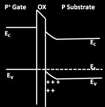

11 NW NEMFET : Basic Device Design and Simulation Zero V G Drain Nanowire Gate oxide Gate Source Accumulation Increase V G Mechanical force Si Ge Electro-static force Pull-In Occurs Depleted


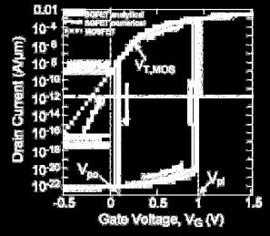
12 Modeling NEMFET device characteristics V DD window on-off ratio within a 0.5V V DD window High I ON /I OFF ratio within 1V DD compared to 4V DD Higher p-doping of the NW leads to high off-current for the stuckstate JH. Kim, C. Chen, DRC (2013)


13 Gen 1 NEMFET: a contact switch Process Flow JH. Kim DRC (2013)


14 Gen 2 NEMFET: back gated V PULL-IN NW diameter : 28nnm L CH : 1.68um t GAP 80nm Gate oxide 40nm ZrO 2 V GS Sweep Direction V PULL-OUT V PI : 10.8V V PO : 6.5V I ON /I OFF : 10.7 S.S. : <15mV 1um JH. Kim DRC (2013)


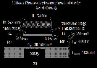
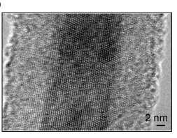
15 Final NEMFET with HfO 2 dielectrics L: 1.3 mm 100 mm x gap : 35 nm D: nm 5 mm Atomic level control of air gap reduction by ALD coating
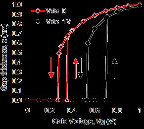
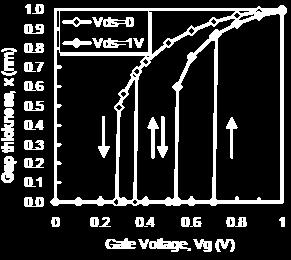
16 Near Zero S.S. at Room Temperature V pi -V po = 1.6 V 12 mv/dec V d = 1 V V pi : 14.48V S.S. : 6 mv/dec (limited by bin size) I on /I off : 2200 (limited by stuck-state off current) I on = 2 ma
 = 0.83±0.52 V Eventually failed due to stiction. JH.")
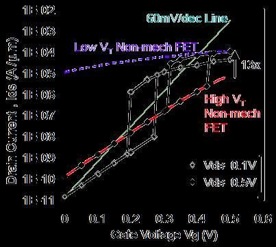
17 Stable, multiple switching with < 1V voltage window Initial rise but stabilized operational voltage window (V pi -V po ) = 0.83±0.52 V Eventually failed due to stiction. JH. Kim (submitted)


18 NEMFET resonance at 126 MHz (VHF) I MIX measurement with 400Hz/99% AM modulation Measured f 0 = 126MHz; Q = 630 at 40 mv drive. Quadratic dependency of f 0 to AC drive voltage


 V ac V g dc GND V.A.")
19 Gate and bias dependence of resonance frequency elucidates how nanowire is tensioned and driven f o vs. V g Elastic Hardening. Nanowire has no slack f o vs. V d Capacitive Softening (Effective side gate effect) V ac V g dc GND V.A. Sazonova Cornell thesis (2006) JH. Kim (submitted)


20 Device Speed and Scaling a design window for Si-based NW NEMFET Airgap fixed at 10 nm. >300 MHz with 5 V V pull-in can be achieved using SiNWs with 11.7 nm diameter. Readily available in our laboratory. Sub 1V operation for diameter smaller than 5 nm. More aggressive scaling with CNT, graphene and other 2D monolayer materials

21 Conclusion Low-Power, High-Speed NEMFET ~ 0 mv/dec S.S. circumvents thermodynamic limit to sharp switching VHF operation with small voltage window requirements (< 1 V) due to nanowire beam structure Can enable both logic and non-volatile memory Next steps: Improvements needed on doping and surface states control in Si/Ge based channels. Further scaling and interface fixed charge planting for reduced V pi. Explore new carbon-based or molecular monolayer materials.
Beyond Transistor Scaling: New Devices for Ultra Low Energy Information Processing
 Beyond Transistor Scaling: New Devices for Ultra Low Energy Information Processing Prof. Tsu Jae King Liu Department of Electrical Engineering and Computer Sciences University of California, Berkeley,
Towards Sub-10 nm Diameter InGaAs Vertical nanowire MOSFETs and TFETs
 Towards Sub-10 nm Diameter InGaAs Vertical nanowire MOSFETs and TFETs J. A. del Alamo, X. Zhao, W. Lu, and A. Vardi Microsystems Technology Laboratories Massachusetts Institute of Technology 5 th Berkeley
III-V CMOS: Quo Vadis?
 III-V CMOS: Quo Vadis? J. A. del Alamo, X. Cai, W. Lu, A. Vardi, and X. Zhao Microsystems Technology Laboratories Massachusetts Institute of Technology Compound Semiconductor Week 2018 Cambridge, MA, May
Depletion-mode operation ( 공핍형 ): Using an input gate voltage to effectively decrease the channel size of an FET
: Using an input gate voltage to effectively decrease the channel size of an FET") Ch. 13 MOSFET Metal-Oxide-Semiconductor Field-Effect Transistor : I D D-mode E-mode V g The gate oxide is made of dielectric SiO 2 with e = 3.9 Depletion-mode operation ( 공핍형 ): Using an input gate voltage
Ch. 13 MOSFET Metal-Oxide-Semiconductor Field-Effect Transistor : I D D-mode E-mode V g The gate oxide is made of dielectric SiO 2 with e = 3.9 Depletion-mode operation ( 공핍형 ): Using an input gate voltage
III-V Vertical Nanowire FETs with Steep Subthreshold Towards Sub-10 nm Diameter Devices
 III-V Vertical Nanowire FETs with Steep Subthreshold Towards Sub-10 nm Diameter Devices Jesús A. del Alamo, Xin Zhao, Wenjie Lu, Alon Vardi Microsystems Technology Laboratories, MIT E 3 S Retreat September
Tunneling Field Effect Transistors for Low Power ULSI
 Tunneling Field Effect Transistors for Low Power ULSI Byung-Gook Park Inter-university Semiconductor Research Center and School of Electrical and Computer Engineering Seoul National University Outline
Parameter Optimization Of GAA Nano Wire FET Using Taguchi Method
 Parameter Optimization Of GAA Nano Wire FET Using Taguchi Method S.P. Venu Madhava Rao E.V.L.N Rangacharyulu K.Lal Kishore Professor, SNIST Professor, PSMCET Registrar, JNTUH Abstract As the process technology
INTERNATIONAL JOURNAL OF APPLIED ENGINEERING RESEARCH, DINDIGUL Volume 1, No 3, 2010
 Low Power CMOS Inverter design at different Technologies Vijay Kumar Sharma 1, Surender Soni 2 1 Department of Electronics & Communication, College of Engineering, Teerthanker Mahaveer University, Moradabad
The Path Toward Efficient Nano-Mechanical Circuits and Systems
 The Path Toward Efficient Nano-Mechanical Circuits and Systems http://www.chi-yun.com/blog/wp-content/uploads/2008/10/ba-road-less.jp Tsu-Jae King Liu 1 Elad Alon 1, Vladimir Stojanovic 2, Dejan Markovic
Transistor Scaling in the Innovation Era. Mark Bohr Intel Senior Fellow Logic Technology Development August 15, 2011
 Transistor Scaling in the Innovation Era Mark Bohr Intel Senior Fellow Logic Technology Development August 15, 2011 MOSFET Scaling Device or Circuit Parameter Scaling Factor Device dimension tox, L, W
Tunnel FET architectures and device concepts for steep slope switches Joachim Knoch
 Tunnel FET architectures and device concepts for steep slope switches Joachim Knoch Institute of Semiconductor Electronics RWTH Aachen University Sommerfeldstraße 24 52074 Aachen Outline MOSFETs Operational
Design of Gate-All-Around Tunnel FET for RF Performance
 Drain Current (µa/µm) International Journal of Computer Applications (97 8887) International Conference on Innovations In Intelligent Instrumentation, Optimization And Signal Processing ICIIIOSP-213 Design
Record I on (0.50 ma/μm at V DD = 0.5 V and I off = 100 na/μm) 25 nm-gate-length ZrO 2 /InAs/InAlAs MOSFETs
 25 nm-gate-length ZrO 2 /InAs/InAlAs MOSFETs") Record I on (0.50 ma/μm at V DD = 0.5 V and I off = 100 na/μm) 25 nm-gate-length ZrO 2 /InAs/InAlAs MOSFETs Sanghoon Lee 1*, V. Chobpattana 2,C.-Y. Huang 1, B. J. Thibeault 1, W. Mitchell 1, S. Stemmer
Record I on (0.50 ma/μm at V DD = 0.5 V and I off = 100 na/μm) 25 nm-gate-length ZrO 2 /InAs/InAlAs MOSFETs Sanghoon Lee 1*, V. Chobpattana 2,C.-Y. Huang 1, B. J. Thibeault 1, W. Mitchell 1, S. Stemmer
Nanoscale III-V CMOS
 Nanoscale III-V CMOS J. A. del Alamo Microsystems Technology Laboratories Massachusetts Institute of Technology SEMI Advanced Semiconductor Manufacturing Conference Saratoga Springs, NY; May 16-19, 2016
MOS Capacitance and Introduction to MOSFETs
 ECE-305: Fall 2016 MOS Capacitance and Introduction to MOSFETs Professor Peter Bermel Electrical and Computer Engineering Purdue University, West Lafayette, IN USA pbermel@purdue.edu 11/4/2016 Pierret,
ECE 340 Lecture 37 : Metal- Insulator-Semiconductor FET Class Outline:
 ECE 340 Lecture 37 : Metal- Insulator-Semiconductor FET Class Outline: Metal-Semiconductor Junctions MOSFET Basic Operation MOS Capacitor Things you should know when you leave Key Questions What is the
Modeling the Influence of Dielectric Interface Traps on I-V Characteristics of TFETs
 Modeling the Influence of Dielectric Interface Traps on I-V Characteristics of TFETs Jie Min 1, Peter Asbeck UCSD 1 Present address: Global Foundries, Santa Clara, CA Schematic TFET Structures Based on
Nanometer-Scale InGaAs Field-Effect Transistors for THz and CMOS Technologies
 Nanometer-Scale InGaAs Field-Effect Transistors for THz and CMOS Technologies J. A. del Alamo Microsystems Technology Laboratories, MIT ESSDERC-ESSCIRC 2013 Bucharest, Romania, September 16-20, 2013 Acknowledgements:
Sub-Threshold Region Behavior of Long Channel MOSFET
 Sub-threshold Region - So far, we have discussed the MOSFET behavior in linear region and saturation region - Sub-threshold region is refer to region where Vt is less than Vt - Sub-threshold region reflects
Integration of III-V heterostructure tunnel FETs on Si using Template Assisted Selective Epitaxy (TASE)
") Integration of III-V heterostructure tunnel FETs on Si using Template Assisted Selective Epitaxy (TASE) K. Moselund 1, D. Cutaia 1. M. Borg 1, H. Schmid 1, S. Sant 2, A. Schenk 2 and H. Riel 1 1 IBM Research
Integration of III-V heterostructure tunnel FETs on Si using Template Assisted Selective Epitaxy (TASE) K. Moselund 1, D. Cutaia 1. M. Borg 1, H. Schmid 1, S. Sant 2, A. Schenk 2 and H. Riel 1 1 IBM Research
Lecture 33 - The Short Metal-Oxide-Semiconductor Field-Effect Transistor (cont.) April 30, 2007
 April 30, 2007") 6.720J/3.43J - Integrated Microelectronic Devices - Spring 2007 Lecture 33-1 Lecture 33 - The Short Metal-Oxide-Semiconductor Field-Effect Transistor (cont.) April 30, 2007 Contents: 1. MOSFET scaling
6.720J/3.43J - Integrated Microelectronic Devices - Spring 2007 Lecture 33-1 Lecture 33 - The Short Metal-Oxide-Semiconductor Field-Effect Transistor (cont.) April 30, 2007 Contents: 1. MOSFET scaling
Design of Nano-Electro Mechanical (NEM) Relay Based Nano Transistor for Power Efficient VLSI Circuits
 Relay Based Nano Transistor for Power Efficient VLSI Circuits") Design of Nano-Electro Mechanical (NEM) Relay Based Nano Transistor for Power Efficient VLSI Circuits Arul C 1 and Dr. Omkumar S 2 1 Research Scholar, SCSVMV University, Kancheepuram, India. 2 Associate
Design of Nano-Electro Mechanical (NEM) Relay Based Nano Transistor for Power Efficient VLSI Circuits Arul C 1 and Dr. Omkumar S 2 1 Research Scholar, SCSVMV University, Kancheepuram, India. 2 Associate
Introduction to VLSI ASIC Design and Technology
 Introduction to VLSI ASIC Design and Technology Paulo Moreira CERN - Geneva, Switzerland Paulo Moreira Introduction 1 Outline Introduction Is there a limit? Transistors CMOS building blocks Parasitics
FinFET-based Design for Robust Nanoscale SRAM
 FinFET-based Design for Robust Nanoscale SRAM Prof. Tsu-Jae King Liu Dept. of Electrical Engineering and Computer Sciences University of California at Berkeley Acknowledgements Prof. Bora Nikoli Zheng
Performance Evaluation of MISISFET- TCAD Simulation
 Performance Evaluation of MISISFET- TCAD Simulation Tarun Chaudhary Gargi Khanna Rajeevan Chandel ABSTRACT A novel device n-misisfet with a dielectric stack instead of the single insulator of n-mosfet
Record Extrinsic Transconductance (2.45 ms/μm at V DS = 0.5 V) InAs/In 0.53 Ga 0.47 As Channel MOSFETs Using MOCVD Source-Drain Regrowth
 InAs/In 0.53 Ga 0.47 As Channel MOSFETs Using MOCVD Source-Drain Regrowth") Record Extrinsic Transconductance (2.45 ms/μm at = 0.5 V) InAs/In 0.53 Ga 7 As Channel MOSFETs Using MOCVD Source-Drain Regrowth Sanghoon Lee 1*, C.-Y. Huang 1, A. D. Carter 1, D. C. Elias 1, J. J. M.
Record Extrinsic Transconductance (2.45 ms/μm at = 0.5 V) InAs/In 0.53 Ga 7 As Channel MOSFETs Using MOCVD Source-Drain Regrowth Sanghoon Lee 1*, C.-Y. Huang 1, A. D. Carter 1, D. C. Elias 1, J. J. M.
Body-Biased Complementary Logic Implemented Using AlN Piezoelectric MEMS Switches
 University of Pennsylvania From the SelectedWorks of Nipun Sinha 29 Body-Biased Complementary Logic Implemented Using AlN Piezoelectric MEMS Switches Nipun Sinha, University of Pennsylvania Timothy S.
Comparative Study of Silicon and Germanium Doping-less Tunnel Field Effect Transistors
 IJSTE - International Journal of Science Technology & Engineering Volume 2 Issue 5 November 2015 ISSN (online): 2349-784X Comparative Study of Silicon and Germanium Doping-less Tunnel Field Effect Transistors
Atomic-layer deposition of ultrathin gate dielectrics and Si new functional devices
 Atomic-layer deposition of ultrathin gate dielectrics and Si new functional devices Anri Nakajima Research Center for Nanodevices and Systems, Hiroshima University 1-4-2 Kagamiyama, Higashi-Hiroshima,
EE70 - Intro. Electronics
 EE70 - Intro. Electronics Course website: ~/classes/ee70/fall05 Today s class agenda (November 28, 2005) review Serial/parallel resonant circuits Diode Field Effect Transistor (FET) f 0 = Qs = Qs = 1 2π
Alternative Channel Materials for MOSFET Scaling Below 10nm
 Alternative Channel Materials for MOSFET Scaling Below 10nm Doug Barlage Electrical Requirements of Channel Mark Johnson Challenges With Material Synthesis Introduction Outline Challenges with scaling
InGaAs MOSFETs for CMOS:
 InGaAs MOSFETs for CMOS: Recent Advances in Process Technology J. A. del Alamo, D. Antoniadis, A. Guo, D.-H. Kim 1, T.-W. Kim 2, J. Lin, W. Lu, A. Vardi and X. Zhao Microsystems Technology Laboratories,
DG-FINFET LOGIC DESIGN USING 32NM TECHNOLOGY
 International Journal of Knowledge Management & e-learning Volume 3 Number 1 January-June 2011 pp. 1-5 DG-FINFET LOGIC DESIGN USING 32NM TECHNOLOGY K. Nagarjuna Reddy 1, K. V. Ramanaiah 2 & K. Sudheer
ECE520 VLSI Design. Lecture 2: Basic MOS Physics. Payman Zarkesh-Ha
 ECE520 VLSI Design Lecture 2: Basic MOS Physics Payman Zarkesh-Ha Office: ECE Bldg. 230B Office hours: Wednesday 2:00-3:00PM or by appointment E-mail: pzarkesh@unm.edu Slide: 1 Review of Last Lecture Semiconductor
Analysis of Power Gating Structure using CNFET Footer
 , October 19-21, 211, San Francisco, USA Analysis of Power Gating Structure using CNFET Footer Woo-Hun Hong, Kyung Ki Kim Abstract This paper proposes a new hybrid MOSFET/ carbon nanotube FET (CNFET) power
Reconfigurable Si-Nanowire Devices
 Reconfigurable Si-Nanowire Devices André Heinzig, Walter M. Weber, Dominik Martin, Jens Trommer, Markus König and Thomas Mikolajick andre.heinzig@namlab.com log I d Present CMOS technology ~ 88 % of IC
Dependence of Carbon Nanotube Field Effect Transistors Performance on Doping Level of Channel at Different Diameters: on/off current ratio
 Copyright (2012) American Institute of Physics. This article may be downloaded for personal use only. Any other use requires prior permission of the author and the American Institute of Physics. The following
A New Self-aligned Quantum-Well MOSFET Architecture Fabricated by a Scalable Tight-Pitch Process
 A New Self-aligned Quantum-Well MOSFET Architecture Fabricated by a Scalable Tight-Pitch Process Jianqiang Lin, Xin Zhao, Tao Yu, Dimitri A. Antoniadis, and Jesús A. del Alamo Microsystems Technology Laboratories,
UNIVERSITY OF CALIFORNIA AT BERKELEY College of Engineering Department of Electrical Engineering and Computer Sciences.
 UNIVERSITY OF CALIFORNIA AT BERKELEY College of Engineering Department of Electrical Engineering and Computer Sciences Discussion #9 EE 05 Spring 2008 Prof. u MOSFETs The standard MOSFET structure is shown
Transport properties of graphene nanoribbon-based tunnel
 Transport properties of graphene nanoribbon-based tunnel Mark Cheung School of Engineering and Applied Science, Department of Electrical and Computer Engineering Keywords: Monolithic Graphene, Low-Power,
CHAPTER 3 PERFORMANCE OF A TWO INPUT NAND GATE USING SUBTHRESHOLD LEAKAGE CONTROL TECHNIQUES
 CHAPTER 3 PERFORMANCE OF A TWO INPUT NAND GATE USING SUBTHRESHOLD LEAKAGE CONTROL TECHNIQUES 41 In this chapter, performance characteristics of a two input NAND gate using existing subthreshold leakage
InGaAs MOSFET Electronics
 InGaAs MOSFET Electronics J. A. del Alamo Microsystems Technology Laboratories, MIT The 17 th International Symposium Physics of Semiconductors and Applications Jeju, Korea, December 7-11, 2014 Acknowledgements:
Session 10: Solid State Physics MOSFET
 Session 10: Solid State Physics MOSFET 1 Outline A B C D E F G H I J 2 MOSCap MOSFET Metal-Oxide-Semiconductor Field-Effect Transistor: Al (metal) SiO2 (oxide) High k ~0.1 ~5 A SiO2 A n+ n+ p-type Si (bulk)
Sub-30 nm InAs Quantum-Well MOSFETs with Self-Aligned Metal Contacts and Sub-1 nm EOT HfO 2 Insulator
 Sub-30 nm InAs Quantum-Well MOSFETs with Self-Aligned Metal Contacts and Sub-1 nm EOT HfO 2 Insulator Jianqiang Lin, Dimitri A. Antoniadis, and Jesús A. del Alamo Microsystems Technology Laboratories,
Leakage Current Analysis
 Current Analysis Hao Chen, Latriese Jackson, and Benjamin Choo ECE632 Fall 27 University of Virginia , , @virginia.edu Abstract Several common leakage current reduction methods such
Gigahertz Ambipolar Frequency Multiplier Based on Cvd Graphene
 Gigahertz Ambipolar Frequency Multiplier Based on Cvd Graphene The MIT Faculty has made this article openly available. Please share how this access benefits you. Your story matters. Citation As Published
Logic circuits based on carbon nanotubes
 Available online at www.sciencedirect.com Physica E 16 (23) 42 46 www.elsevier.com/locate/physe Logic circuits based on carbon nanotubes A. Bachtold a;b;, P. Hadley a, T. Nakanishi a, C. Dekker a a Department
Study of Pattern Area of Logic Circuit. with Tunneling Field-Effect Transistors
 Contemporary Engineering Sciences, Vol. 6, 2013, no. 6, 273-284 HIKARI Ltd, www.m-hikari.com http://dx.doi.org/10.12988/ces.2013.3632 Study of Pattern Area of Logic Circuit with Tunneling Field-Effect
ECE 5745 Complex Digital ASIC Design Topic 2: CMOS Devices
 ECE 5745 Complex Digital ASIC Design Topic 2: CMOS Devices Christopher Batten School of Electrical and Computer Engineering Cornell University http://www.csl.cornell.edu/courses/ece5950 Simple Transistor
Low Power Realization of Subthreshold Digital Logic Circuits using Body Bias Technique
 Indian Journal of Science and Technology, Vol 9(5), DOI: 1017485/ijst/2016/v9i5/87178, Februaru 2016 ISSN (Print) : 0974-6846 ISSN (Online) : 0974-5645 Low Power Realization of Subthreshold Digital Logic
Practical Information
 EE241 - Spring 2013 Advanced Digital Integrated Circuits MW 2-3:30pm 540A/B Cory Practical Information Instructor: Borivoje Nikolić 509 Cory Hall, 3-9297, bora@eecs Office hours: M 11-12, W 3:30pm-4:30pm
Contribution of Gate Induced Drain Leakage to Overall Leakage and Yield Loss in Digital submicron VLSI Circuits
 Contribution of Gate Induced Drain Leakage to Overall Leakage and Yield Loss in Digital submicron VLSI Circuits Oleg Semenov, Andrzej Pradzynski * and Manoj Sachdev Dept. of Electrical and Computer Engineering,
NAME: Last First Signature
 UNIVERSITY OF CALIFORNIA, BERKELEY College of Engineering Department of Electrical Engineering and Computer Sciences EE 130: IC Devices Spring 2003 FINAL EXAMINATION NAME: Last First Signature STUDENT
FUNDAMENTALS OF MODERN VLSI DEVICES
 19-13- FUNDAMENTALS OF MODERN VLSI DEVICES YUAN TAUR TAK H. MING CAMBRIDGE UNIVERSITY PRESS Physical Constants and Unit Conversions List of Symbols Preface page xi xiii xxi 1 INTRODUCTION I 1.1 Evolution
Silicon Single-Electron Devices for Logic Applications
 ESSDERC 02/9/25 Silicon Single-Electron Devices for Logic Applications NTT Basic Research Laboratories Yasuo Takahashi Collaborators: : Yukinori Ono, Akira Fujiwara, Hiroshi Inokawa, Kenji Shiraishi, Masao
ANALYTICAL MODELING AND CHARACTERIZATION OF CYLINDRICAL GATE ALL AROUND MOSFET
 ANALYTICAL MODELING AND CHARACTERIZATION OF CYLINDRICAL GATE ALL AROUND MOSFET Shailly Garg 1, Prashant Mani Yadav 2 1 Student, SRM University 2 Assistant Professor, Department of Electronics and Communication,
Semiconductor Physics and Devices
 Nonideal Effect The experimental characteristics of MOSFETs deviate to some degree from the ideal relations that have been theoretically derived. Semiconductor Physics and Devices Chapter 11. MOSFET: Additional
Leakage Current in Low Standby Power and High Performance Devices: Trends and Challenges
 Leakage Current in Low Standby Power and High Performance Devices: Trends and Challenges (Invited Paper) Geoffrey C-F Yeap Motorola Inc., DigitalDNA Laboratories, 3501 Ed Bluestein Blvd., MD: K10, Austin,
Fin-Shaped Field Effect Transistor (FinFET) Min Ku Kim 03/07/2018
 Min Ku Kim 03/07/2018") Fin-Shaped Field Effect Transistor (FinFET) Min Ku Kim 03/07/2018 ECE 658 Sp 2018 Semiconductor Materials and Device Characterizations OUTLINE Background FinFET Future Roadmap Keeping up w/ Moore s Law
Fin-Shaped Field Effect Transistor (FinFET) Min Ku Kim 03/07/2018 ECE 658 Sp 2018 Semiconductor Materials and Device Characterizations OUTLINE Background FinFET Future Roadmap Keeping up w/ Moore s Law
Optimization of Direct Tunneling Gate Leakage Current in Ultrathin Gate Oxide FET with High-K Dielectrics
 Optimization of Direct Tunneling Gate Leakage Current in Ultrathin Gate Oxide FET with High-K Dielectrics Sweta Chander 1, Pragati Singh 2, S Baishya 3 1,2,3 Department of Electronics & Communication Engineering,
Active Technology for Communication Circuits
 EECS 242: Active Technology for Communication Circuits UC Berkeley EECS 242 Copyright Prof. Ali M Niknejad Outline Comparison of technology choices for communication circuits Si npn, Si NMOS, SiGe HBT,
Week 9a OUTLINE. MOSFET I D vs. V GS characteristic Circuit models for the MOSFET. Reading. resistive switch model small-signal model
 Week 9a OUTLINE MOSFET I vs. V GS characteristic Circuit models for the MOSFET resistive switch model small-signal model Reading Rabaey et al.: Chapter 3.3.2 Hambley: Chapter 12 (through 12.5); Section
Comparison of 32nm High-k Metal Gate Predictive Technology Model CMOS and MOSFET-Like CNFET compact Model Based Domino logic Circuits
 Comparison of 32nm High-k Metal Gate Predictive Technology Model CMOS and MOSFET-Like CNFET compact Model Based Domino logic Circuits Saravana Maruthamuthu, Wireless Group Infineon Technologies India Private
FACULTY OF ENGINEERING LAB SHEET ENT 3036 SEMICONDUCTOR DEVICES TRIMESTER
 FACULTY OF ENGINEERING LAB SHEET ENT 3036 SEMICONDUCTOR DEVICES TRIMESTER 3 2017-2018 SD1 I-V MEASUREMENT OF MOS CAPACITOR *Note: On-the-spot evaluation may be carried out during or at the end of the experiment.
Transparent p-type SnO Nanowires with Unprecedented Hole Mobility among Oxide Semiconductors
 Supplementary Information Transparent p-type SnO Nanowires with Unprecedented Hole Mobility among Oxide Semiconductors J. A. Caraveo-Frescas and H. N. Alshareef* Materials Science and Engineering, King
Vertical Nanowire InGaAs MOSFETs Fabricated by a Top-down Approach
 Vertical Nanowire InGaAs MOSFETs Fabricated by a Top-down Approach Xin Zhao, Jianqiang Lin, Christopher Heidelberger, Eugene A. Fitzgerald and Jesús A. del Alamo Microsystems Technology Laboratories, MIT
Acknowledgments: This work was supported by Air Force HiREV program and the DTRA Basic Research Program.
 Gate Bias and Geometry Dependence of Total-Ionizing-Dose Effects in InGaAs Quantum-Well MOSFETs K. Ni 1, E. X. Zhang 1, R. D. Schrimpf 1, D. M. Fleetwood 1, R. A. Reed 1, M. L. Alles 1, J. Lin 2, and J.
Performance Optimization of Dynamic and Domino logic Carry Look Ahead Adder using CNTFET in 32nm technology
 IOSR Journal of VLSI and Signal Processing (IOSR-JVSP) Volume 5, Issue 5, Ver. I (Sep - Oct. 2015), PP 30-35 e-issn: 2319 4200, p-issn No. : 2319 4197 www.iosrjournals.org Performance Optimization of Dynamic
Experimentally reported sub-60mv/dec
 Experimentally reported sub-60mv/dec swing in Tunnel FETs? 1 We considered InAs conventional, lateral transistor architectures: GAA nanowire, Fin FETs FETs (Tri gate) UTB,DG SOI Analysis is not directly
The 3 D Tri Gate transistor is a variant of the FinFET developed at UC Berkeley, and is being used in Intel s 22nmgeneration. microprocessors.
 On May 4, 2011, Intel Corporation announced what it called the most radical shift in semiconductor technology in 50 years. A new 3 dimensional transistor design will enable the production of integrated
CHAPTER 2 LITERATURE REVIEW
 CHAPTER 2 LITERATURE REVIEW 2.1 Introduction of MOSFET The structure of the MOS field-effect transistor (MOSFET) has two regions of doping opposite that of the substrate, one at each edge of the MOS structure
Design & Performance Analysis of DG-MOSFET for Reduction of Short Channel Effect over Bulk MOSFET at 20nm
 RESEARCH ARTICLE OPEN ACCESS Design & Performance Analysis of DG- for Reduction of Short Channel Effect over Bulk at 20nm Ankita Wagadre*, Shashank Mane** *(Research scholar, Department of Electronics
Performance advancement of High-K dielectric MOSFET
 Performance advancement of High-K dielectric MOSFET Neha Thapa 1 Lalit Maurya 2 Er. Rajesh Mehra 3 M.E. Student M.E. Student Associate Prof. ECE NITTTR, Chandigarh NITTTR, Chandigarh NITTTR, Chandigarh
InGaAs Nanoelectronics: from THz to CMOS
 InGaAs Nanoelectronics: from THz to CMOS J. A. del Alamo Microsystems Technology Laboratories, MIT IEEE International Conference on Electron Devices and Solid-State Circuits Hong Kong, June 3, 2013 Acknowledgements:
Performance of Near-Ballistic Limit Carbon Nano Transistor (CNT) Circuits
 Circuits") Performance of Near-Ballistic Limit Carbon Nano Transistor (CNT) Circuits A. A. A. Nasser 1, Moustafa H. Aly 2, Roshdy A. AbdelRassoul 3, Ahmed Khourshed 4 College of Engineering and Technology, Arab Academy
Performance of Near-Ballistic Limit Carbon Nano Transistor (CNT) Circuits A. A. A. Nasser 1, Moustafa H. Aly 2, Roshdy A. AbdelRassoul 3, Ahmed Khourshed 4 College of Engineering and Technology, Arab Academy
A Review Of Conventional And Emerging Power Gating Techniques For Leakage Power Reduction
 A Review Of Conventional And Emerging Power Gating Techniques For Leakage Power Reduction Sandip B. Rahane, A.K. Kureshi, Sachin D. Pable Abstract Leakage power reduction has become one of the top design
Zota, Cezar B.; Lindelow, Fredrik; Wernersson, Lars Erik; Lind, Erik
 InGaAs tri-gate MOSFETs with record on-current Zota, Cezar B.; Lindelow, Fredrik; Wernersson, Lars Erik; Lind, Erik Published in: 6 IEEE International Electron Devices Meeting, IEDM 6 DOI:.9/IEDM.6.7886
Nanoelectronics and the Future of Microelectronics
 Nanoelectronics and the Future of Microelectronics Mark Lundstrom Electrical and Computer Engineering University, West Lafayette, IN August 22, 2002 1. Introduction 2. Challenges in Silicon Technology
DESIGN OF ON CHIP TEMPERATURE MONITORING IN 90NM CMOS
 DESIGN OF ON CHIP TEMPERATURE MONITORING IN 90NM CMOS A thesis submitted to the faculty of San Francisco State University In partial fulfillment of The Requirements for The Degree Master of Science In
III-V Channel Transistors
 III-V Channel Transistors Jesús A. del Alamo Professor Microsystems Technology Laboratories MIT Acknowledgements: Students and collaborators: D. Antoniadis, J. Lin, W. Lu, A. Vardi, X. Zhao Sponsors: Applied
A BRIEF STUDY ON CHALLENGES OF MOSFET AND EVOLUTION OF FINFETS
 A BRIEF STUDY ON CHALLENGES OF MOSFET AND EVOLUTION OF FINFETS ABSTRACT J.Shailaja 1, Y.Priya 2 1 ECE Department, Sphoorthy Engineering College (India) 2 ECE,Sphoorthy Engineering College, (India) The
Low Power Design of Schmitt Trigger Based SRAM Cell Using NBTI Technique
 Low Power Design of Schmitt Trigger Based SRAM Cell Using NBTI Technique M.Padmaja 1, N.V.Maheswara Rao 2 Post Graduate Scholar, Gayatri Vidya Parishad College of Engineering for Women, Affiliated to JNTU,
Fundamental Tradeoff between Conductance and Subthreshold Swing Voltage for Barrier Thickness Modulation in Tunnel Field Effect Transistors
 Fundamental Tradeoff between Conductance and Subthreshold Swing Voltage for Barrier Thickness Modulation in Tunnel Field Effect Transistors Sapan Agarwal Eli Yablonovitch Electrical Engineering and Computer
Semiconductor Memory: DRAM and SRAM. Department of Electrical and Computer Engineering, National University of Singapore
 Semiconductor Memory: DRAM and SRAM Outline Introduction Random Access Memory (RAM) DRAM SRAM Non-volatile memory UV EPROM EEPROM Flash memory SONOS memory QD memory Introduction Slow memories Magnetic
Low Power Design of Successive Approximation Registers
 Low Power Design of Successive Approximation Registers Rabeeh Majidi ECE Department, Worcester Polytechnic Institute, Worcester MA USA rabeehm@ece.wpi.edu Abstract: This paper presents low power design
Sustaining the Si Revolution: From 3D Transistors to 3D Integration
 Sustaining the Si Revolution: From 3D Transistors to 3D Integration Tsu Jae King Liu Department of Electrical Engineering and Computer Sciences University of California, Berkeley, CA USA February 23, 2015
EECS 427 Lecture 13: Leakage Power Reduction Readings: 6.4.2, CBF Ch.3. EECS 427 F09 Lecture Reminders
 EECS 427 Lecture 13: Leakage Power Reduction Readings: 6.4.2, CBF Ch.3 [Partly adapted from Irwin and Narayanan, and Nikolic] 1 Reminders CAD assignments Please submit CAD5 by tomorrow noon CAD6 is due
EEC 216 Lecture #8: Leakage. Rajeevan Amirtharajah University of California, Davis
 EEC 216 Lecture #8: Leakage Rajeevan Amirtharajah University of California, Davis Outline Announcements Review: Low Power Interconnect Finish Lecture 7 Leakage Mechanisms Circuit Styles for Low Leakage
Investigation of Feasibility of Tunneling Field Effect Transistor (TFET) as Highly Sensitive and Multi-sensing Biosensors
 as Highly Sensitive and Multi-sensing Biosensors") JOURNAL OF SEMICONDUCTOR TECHNOLOGY AND SCIENCE, VOL.17, NO.1, FEBRUARY, 2017 ISSN(Print) 1598-1657 https://doi.org/10.5573/jsts.2017.17.1.141 ISSN(Online) 2233-4866 Investigation of Feasibility of Tunneling
JOURNAL OF SEMICONDUCTOR TECHNOLOGY AND SCIENCE, VOL.17, NO.1, FEBRUARY, 2017 ISSN(Print) 1598-1657 https://doi.org/10.5573/jsts.2017.17.1.141 ISSN(Online) 2233-4866 Investigation of Feasibility of Tunneling
ENG2410 Digital Design CMOS Technology. Fall 2017 S. Areibi School of Engineering University of Guelph
 ENG2410 Digital Design CMOS Technology Fall 2017 S. reibi School of Engineering University of Guelph The Transistor Revolution First transistor Bell Labs, 1948 Bipolar logic 1960 s Intel 4004 processor
The Design of SET-CMOS Hybrid Logic Style of 1-Bit Comparator
 The Design of SET-CMOS Hybrid Logic Style of 1-Bit Comparator A. T. Fathima Thuslim Department of Electronics and communication Engineering St. Peters University, Avadi, Chennai, India Abstract: Single
Practical Information
 EE241 - Spring 2010 Advanced Digital Integrated Circuits TuTh 3:30-5pm 293 Cory Practical Information Instructor: Borivoje Nikolić 550B Cory Hall, 3-9297, bora@eecs Office hours: M 10:30am-12pm Reader:
DESIGN AND ANALYSIS OF SUB 1-V BANDGAP REFERENCE (BGR) VOLTAGE GENERATORS FOR PICOWATT LSI s.
 VOLTAGE GENERATORS FOR PICOWATT LSI s.") http:// DESIGN AND ANALYSIS OF SUB 1-V BANDGAP REFERENCE (BGR) VOLTAGE GENERATORS FOR PICOWATT LSI s. Shivam Mishra 1, K. Suganthi 2 1 Research Scholar in Mech. Deptt, SRM University,Tamilnadu 2 Asst.
http:// DESIGN AND ANALYSIS OF SUB 1-V BANDGAP REFERENCE (BGR) VOLTAGE GENERATORS FOR PICOWATT LSI s. Shivam Mishra 1, K. Suganthi 2 1 Research Scholar in Mech. Deptt, SRM University,Tamilnadu 2 Asst.
Performance Analysis of 20 nm Pentagonal and Trapezoidal NanoWire Transistor with Si and Ge Channel
 Performance Analysis of 20 nm Pentagonal and Trapezoidal NanoWire Transistor with Si and Ge Channel SANDEEP SINGH GILL 1, JAIDEV KAUSHIK 2, NAVNEET KAUR 3 Department of Electronics and Communication Engineering
A NEW APPROACH FOR DELAY AND LEAKAGE POWER REDUCTION IN CMOS VLSI CIRCUITS
 http:// A NEW APPROACH FOR DELAY AND LEAKAGE POWER REDUCTION IN CMOS VLSI CIRCUITS Ruchiyata Singh 1, A.S.M. Tripathi 2 1,2 Department of Electronics and Communication Engineering, Mangalayatan University
Vertical InAs/GaAsSb/GaSb tunneling field-effect transistor on Si with S = 48 mv/decade and Ion = 10 A/m for Ioff = 1 na/m at VDS = 0.
 Vertical InAs/GaAsSb/GaSb tunneling field-effect transistor on Si with S = 48 mv/decade and Ion = 10 A/m for Ioff = 1 na/m at VDS = 0.3 V Memisevic, E.; Svensson, Johannes; Hellenbrand, Markus; Lind, Erik;
Leakage Modeling for Devices with Steep Sub-threshold Slope Considering Random Threshold Variations
 Leakage Modeling for Devices with Steep Sub-threshold Slope Considering Random Threshold Variations Ayan Paul, Chaitanya Kshirsagar, Sachin S. Sapatnekar, Steven Koester and Chris H. Kim Electrical and
Optimization of Double Gate Vertical Channel Tunneling Field Effect Transistor (DVTFET) with Dielectric Sidewall
 with Dielectric Sidewall") JOURNAL OF SEMICONDUCTOR TECHNOLOGY AND SCIENCE, VOL.17, NO.2, APRIL, 2017 ISSN(Print) 1598-1657 https://doi.org/10.5573/jsts.2017.17.2.192 ISSN(Online) 2233-4866 Optimization of Double Gate Vertical Channel
JOURNAL OF SEMICONDUCTOR TECHNOLOGY AND SCIENCE, VOL.17, NO.2, APRIL, 2017 ISSN(Print) 1598-1657 https://doi.org/10.5573/jsts.2017.17.2.192 ISSN(Online) 2233-4866 Optimization of Double Gate Vertical Channel
3. COMPARING STRUCTURE OF SINGLE GATE AND DOUBLE GATE MOSFET WITH DESIGN AND CURVE
 P a g e 80 Available online at http://arjournal.org APPLIED RESEARCH JOURNAL RESEARCH ARTICLE ISSN: 2423-4796 Applied Research Journal Vol. 3, Issue, 2, pp.80-86, February, 2017 COMPARATIVE STUDY ON SINGLE
Department of Electrical Engineering IIT Madras
 Department of Electrical Engineering IIT Madras Sample Questions on Semiconductor Devices EE3 applicants who are interested to pursue their research in microelectronics devices area (fabrication and/or