III-V Channel Transistors
|
|
|
- Damon Robertson
- 5 years ago
- Views:
Transcription


1 III-V Channel Transistors Jesús A. del Alamo Professor Microsystems Technology Laboratories MIT Acknowledgements: Students and collaborators: D. Antoniadis, J. Lin, W. Lu, A. Vardi, X. Zhao Sponsors: Applied Materials, DTRA, KIST, Lam Research, Northrop Grumman, NSF, Samsung Labs at MIT: MTL, EBL 24 April 2017


2 Moore s Law at 50: the end in sight? 2

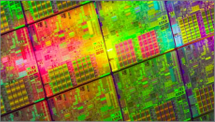
3 Moore s Law Moore s Law = exponential increase in transistor density Intel microprocessors 2016: Intel 22-core Xeon Broadwell-E5 7.2B transistors 3
4 Moore s Law How far can Si support Moore s Law?? 4
5 Transistor scaling Voltage scaling Performance suffers Supply voltage: Transistor current density: Intel microprocessors Intel microprocessors Goals: Reduced footprint with moderate short-channel effects High performance at low voltage 5

6 Moore s Law: it s all about MOSFET scaling 1. New device structures with improved scalability: 2. New materials with improved transport characteristics: n-channel: Si Strained Si SiGe InGaAs p-channel: Si Strained Si SiGe Ge InGaSb 6

7 III-V electronics in your pocket! 7


8 Contents 8


9 1. Self-aligned Planar InGaAs MOSFETs dry-etched recess selective MOCVD W Mo Lin, IEDM 2012, 2013, 2014 Lee, EDL 2014; Huang, IEDM 2014 implanted Si + selective epi reacted NiInAs Sun, IEDM 2013, 2014 Chang, IEDM
 1.0 L g =20 nm V gs -V t = 0.5 V 0.8 R on =224 m 0.4 V 0.6 0.4 0.2 0.0 0.0 0.1 0.2 0.3 0.4 0.5 V ds (V) 10")
10 Self-aligned Planar InGaAs MIT W Mo Lin, IEDM 2012, 2013, 2014 Recess-gate process: CMOS-compatible Refractory ohmic contacts Extensive use of RIE I d (ma/ m) 1.0 L g =20 nm V gs -V t = 0.5 V 0.8 R on =224 m 0.4 V V ds (V) 10


 dimensions MOS interface exposed late")
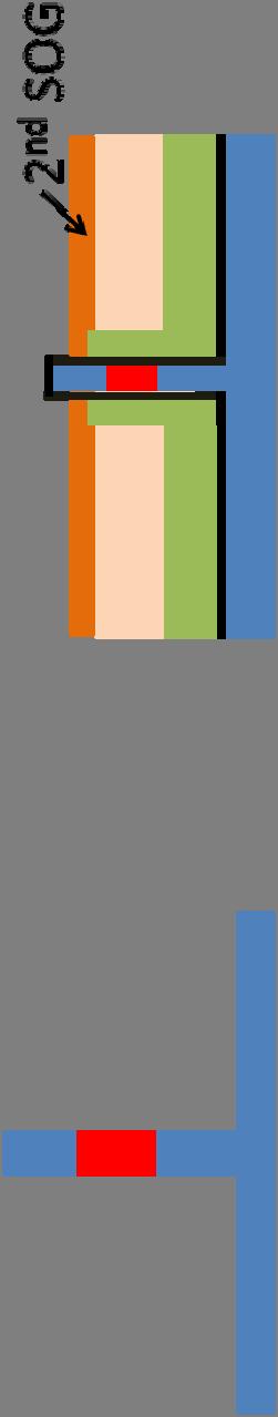
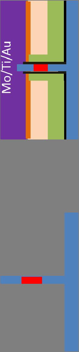
11 Fabrication process Mo/W ohmic contact + SiO 2 hardmask SF 6, CF 4 anisotropic RIE Resist CF 4 :O 2 isotropic RIE SiO 2 W/Mo n + InGaAs/InP InGaAs/InAs InAlAs -Si InP Waldron, IEDM 2007 Cl 2 :N 2 anisotropic RIE Digital etch Finished device O 2 plasma H 2 SO 4 Pad Mo HfO 2 Lin, EDL 2014 Ohmic contact first, gate last Precise control of vertical (~1 nm), lateral (~5 nm) dimensions MOS interface exposed late in process 11

 Gate oxide:")


12 Highest performance InGaAs MOSFET Channel: In 0.7 Ga 0.3 As/InAs/In 0.7 Ga 0.3 As (t ch =9 nm) Gate oxide: HfO 2 (2.5 nm, EOT~ 0.5 nm) 3.45 ms/ m L g =70 nm: Exceeds best HEMT! Record g m,max = 3.45 ms/µm at V ds = 0.5 V R on = 190 Ω.µm Lin, EDL

13 Excess OFF-state current Transistor fails to turn off: I d (A/ m) 10-5 L g =500 nm V ds V ds =0.3~0.7 V step=50 mv V gs (V) OFF-state current enhanced with V ds Band-to-Band Tunneling (BTBT) or Gate-Induced Drain Leakage (GIDL) Lin, IEDM
14 Excess OFF-state current I d (A/ m) T=200 K V ds =0.7 V L g =80 nm 120 nm 280 nm 500 nm V gs -V t (V) Lin, EDL 2014 Lin, TED 2015 L g OFF-state current bipolar gain effect due to floating body I d (A/ m) I d (A/ m) 10-5 L g =500 nm w/ W/ BTBT+BJT w/o W/O BTBT+BJT L g =500 nm V ds V ds =0.3~0.7 V step=50 mv V gs (V) Simulations V ds =0.3~0.7 V step=50 mv V gs (V) 14


15 2. InGaAs FinFETs Intel Si Trigate MOSFETs 15


16 Bottom-up InGaAs FinFETs Aspect-Ratio Trapping Fiorenza, ECST 2010 Si Epi-grown fin inside trench Waldron, VLSI Tech

17 Top-down InGaAs FinFETs Radosavljevic, IEDM 2010 dry-etched fins 60 nm Kim, IEDM
18 Natarajan, IEDM 2014 g m [ms/ m] FinFET benchmarking g m normalized by width of gate periphery Si FinFETs channel aspect ratio InGaAs FinFETs W f [nm] State-of-the-art Si FinFETs: W f =7 nm 18

![m] 2.0 1.5 1.0 0.](/docs-images/85/92444901/images/19-1.jpg "5 FinFET benchmarking g m")


19 Kim, IEDM 2013 Natarajan, IEDM 2014 Oxland, EDL 2016 g m [ms/ m] FinFET benchmarking g m normalized by width of gate periphery Si FinFETs InGaAs FinFETs W f [nm] channel aspect ratio Narrowest InGaAs FinFET fin: W f =15 nm Best channel aspect ratio of InGaAs FinFET: 1.8 g m much lower than planar InGaAs MOSFETs Radosavljevic, IEDM 2011 Thathachary, VLSI

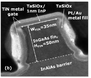
20 InGaAs MIT Key enabling technologies: BCl 3 /SiCl 4 /Ar RIE + digital etch Sub-10 nm fin width Aspect ratio > 20 Vertical sidewalls Vardi, DRC 2014, EDL 2015, IEDM

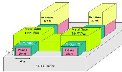
21 InGaAs MIT High K SiO 2 W/Mo n + InGaAs L g Mo HSQ InGaAs δ Si InAlAs InP HSQ High K InGaAs Mo InP Vardi, VLSI Tech 2016 Vardi, EDL 2016 CMOS compatible process Mo contact-first process Fin etch mask left in place double-gate MOSFET 21
![Most aggressively scaled FinFET W f =7 nm, L g =30 nm, H c =40 nm (AR=5.7), EOT=0.6 nm: 1E-3 1E-4 V DS =500 mv I d [ A/ m] 500 400 300 200 V GS =-0.5 to 0.75 V GS =0.](/docs-images/85/92444901/images/22-0.jpg "25 V I d [A/ m] 1E-5 1E-6 1E-7 1E-8 DIBL=90 mv/v S sat =100 mv/dev V DS =50 mv 100 0 0.0 0.1 0.2 0.3 0.4 0.5 V DS [V] 1E-9-0.5-0.4-0.3-0.2-0.1 0.0 0.1 0.2 0.3 0.4 1000 V GS [V] g m max =900 S/ m Current normalized by 2xH c At V DS =0.")
22 Most aggressively scaled FinFET W f =7 nm, L g =30 nm, H c =40 nm (AR=5.7), EOT=0.6 nm: 1E-3 1E-4 V DS =500 mv I d [ A/ m] V GS =-0.5 to 0.75 V GS =0.25 V I d [A/ m] 1E-5 1E-6 1E-7 1E-8 DIBL=90 mv/v S sat =100 mv/dev V DS =50 mv V DS [V] 1E V GS [V] g m max =900 S/ m Current normalized by 2xH c At V DS =0.5 V: g m =900 µs/µm R on =320 Ω.µm g m [ S/ m] V DS =0.5 V Vardi, EDL S sat =100 mv/dec V GS [V] 22
23 L g and EOT scaling g m [ S/ m] EOT V DS =0.5 V W f nm S sat [mv/dec] A: Al 2 O 3, EOT=2.8 nm B:Al 2 O 3 /HfO 2, EOT=1 nm C: HfO 2, EOT=0.6 nm EOT 60 mv/dec L g [nm] L g [nm] V T [V] I on [ A/ m] EOT I off =100 na/ m V DS =0.5 V -0.6 EOT L g [nm] L g [nm] Classical scaling with L g and EOT 23
24 g m max [ S/ m] V T [V] Fin width scaling (EOT=0.6 nm) W f =22 nm W f = 5 nm L g [nm] L g [nm] W f = 5 nm W f =22 nm S sat,min [mv/dec] W f =7 nm W f =12 nm W f =17 nm W f =22 nm L g [nm] Contaminated by gate leakage 60 mv/dec Non-ideal fin width scaling High D it (~5x10 12 cm -2.eV -1 ); mobility degradation; line edge roughness R on [ m] L g [nm] 7 nm W f =22 nm 24
25 InGaAs FinFETs: g m benchmarking g m normalized by width of gate periphery: H c W f H c Double gate Trigate g m [ms/ m] Si FinFETs InGaAs FinFETs W f [nm] First InGaAs FinFETs with W f <10 nm Record results for InGaAs FinFETs with W f < 25 nm Still short of Si FinFETs (though they operate at V DD =0.8 V) 25
26 InGaAs FinFETs: g m benchmarking g m normalized by fin width (FOM for density): H c W f W f H c Vardi, EDL 2016 g m /W f [ms/ m] Si FinFETs (V DD =0.8 V) InGaAs FinFETs W f [nm] Doubled g m /W f over earlier InGaAs FinFETs 26
27 Impact of fin width on V T InGaAs doped-channel FinFETs: 50 nm thick, N D ~10 18 cm -3 Vardi, IEDM 2015 T=90K Strong V T sensitivity for W f < 10 nm; much worse than Si Due to quantum effects Big concern for future manufacturing 27

28 3. Vertical nanowire MOSFET: ultimate scalable transistor L L c spacer L g Vertical NW MOSFET: uncouples footprint scaling from L g, L spacer, and L c scaling 28


29 Vertical nanowire MOSFET for 5 nm node 5 nm node Yakimets, TED 2015 Bao, ESSDERC % area reduction in 6T SRAM 19% area reduction in 32 bit multiplier Vertical NW: power, performance and area gains w.r.t. Lateral NW or FinFET 29


 Technique")

30 InGaAs Vertical Nanowires on Si by direct growth Au seed InAs NWs on Si by SAE Vapor-Solid-Liquid (VLS) Technique Selective-Area Epitaxy Riel, MRS Bull 2014 Björk, JCG

31 InGaAs VNW MOSFETs by top-down MIT Key enabling technologies: RIE = BCl 3 /SiCl 4 /Ar chemistry Digital Etch (DE) = O 2 plasma oxidation H 2 SO 4 oxide removal 240 nm 15 nm Sub-20 nm NW diameter Aspect ratio > 10 Smooth sidewalls Zhao, EDL
32 InGaAs VNW Mechanical Stability for D<10 nm Difficult to reach 10 nm VNW diameter due to breakage 8 nm InGaAs VNWs: Yield = 0% Broken NW 32
33 InGaAs VNW Mechanical Stability for D<10 nm Difficult to reach 10 nm VNW diameter due to breakage Broken NW 8 nm InGaAs VNWs: Yield = 0% Water-based acid is problem: Surface tension (mn/m): Water: 72 Methanol: 22 IPA: 23 Solution: alcohol-based digital etch 33


34 Alcohol-Based Digital Etch 8 nm InGaAs VNWs Lu, EDL % HCl in DI water Yield = 0% 10% HCl in IPA Yield = 97% Broken NW Radial etch rate: 1.0 nm/cycle Radial etch rate: 1.0 nm/cycle Alcohol-based DE enables D < 10 nm 34
 Lu, EDL 2017")
35 InGaAs Digital Etch First demonstration of D=5 nm diameter InGaAs VNW (Aspect Ratio > 40) Lu, EDL

36 InGaAs VNW-MOSFETs by top-down MIT Starting heterostructure: n + InGaAs, 70 nm i InGaAs, 80 nm n + InGaAs, 300 nm n + : cm 3 Si doping Top-down approach: flexible and manufacturable 36


37 Tomioka, Nature 2012 Persson, DRC 2012 Zhao, IEDM 2013 Process flow 37
38 NW-MOSFET I-V characteristics: D=40 nm I s A/ m) 300 V gs =-0.2 V to 0.7 V in 0.1 V step V ds (V) g m ( S/ m) V d = 0.5 V g m,pk =720 μs/μm Zhao, CSW V gs (V) 10-3 V ds =0.5 V Single nanowire MOSFET: L ch = 80 nm 3 nm Al 2 O 3 (EOT = 1.5 nm) g m,pk =720 V DS =0.5 V S lin =70 mv/dec, S sat =80 mv/dec DIBL=88 mv/v I s (A/ m) V ds =0.05 V S lin = 70 mv/dec S sat = 80 mv/dec DIBL = 88 mv/v V gs (V) 38
 1400 1200")


39 InGaAs VNW-MOSFETs Benchmark Berg, IEDM 2015 Tomioka, Nature 2012 g m,pk ( S/ m) V ds =0.5 V This work Tanaka, APEX 2010 Tomioka, IEDM 2011 Tomioka, Nature 2012 Persson, DRC 2012 Persson, EDL 2010 Zhao, IEDM 2013 Berg, IEDM 2015 This work S sat (mv/dec) Persson, DRC 2012 Tanaka, APEX 2010 Top down VNW MOSFETs as good as bottom up devices 39
40 How are we doing in terms of short-channel effects? Planar-MOSFET FinFET S lin : linear subthreshold swing L g = gate length λ c = electrostatic scaling length: f(t ox, t ch ) Ideal scaling VNW MOSFET Reasonable scaling behavior but Excessive D it del Alamo, J-EDS


41 4. InGaSb p type MOSFETs Planar InGaSb MOSFET demonstrations: Nainani, IEDM 2010 Takei, Nano Lett


42 InGaSb p type MIT Key enabling technology: BCl 3 /N 2 RIE [digital etch under development] 20 nm fins, 20 nm spacing Lu, IEDM nm fins, AR>13 Smallest W f = 15 nm Aspect ratio >10 Fin angle > 85 Dense fin patterns 42
43 Si-compatible contacts to p + -InAs Ni/Ti/Pt/Al on p + -InAs (circular TLMs): Lu, IEDM 2015 Record ρ c : 3.5x10⁻⁸ Ω.cm 2 at 400 o C 43


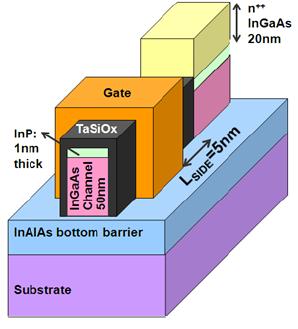
44 InGaSb p-type FinFETs Fin etch mask left in place double-gate MOSFET Channel: 10 nm In 0.27 Ga 0.73 Sb (compressively strained) Gate oxide: 4 nm Al 2 O 3 (EOT=1.8 nm) Lu, IEDM
 Normalized by conducting gate periphery First InGaSb FinFET Peak g m approaches best InGaSb planar MOSFETs Poor turn off g m ( S/ m) 100 This work (FinFET) In 0.27 Ga 0.")
45 InGaSb FinFET I-V characteristics L g = 100 nm, W f = 30 nm (AR=0.33) Normalized by conducting gate periphery First InGaSb FinFET Peak g m approaches best InGaSb planar MOSFETs Poor turn off g m ( S/ m) 100 This work (FinFET) In 0.27 Ga 0.73 Sb Planar MOSFETs Yuan, 2013 [7] Nainani, 2010 [8] Chu, 2014 [11] Xu, 2011 [12] Nagaiah, 2011 [13] GaSb GaSb In 0.36 Ga 0.64 Sb L g ( m) In 0.35 Ga 0.65 Sb In 0.2 Ga 0.8 Sb Lu, IEDM
46 InGaSb p-channel FinFETs (2 nd gen.) 200 L g = 100 nm, W f = 18 nm (AR=0.42) Channel: 7.5 nm In 0.4 Ga 0.6 Sb V g : 1 to -1.6 in -0.4V step, R tot :2.30e+03 - m Lu, CSW V d (V) g m ( S/ m) g m,max = 200 µs/µm Still poor turn-off need digital etch, better sidewall passivation 100 Gen 1 In 0.27 Ga 0.73 Sb Gen 1 In 0.2 Ga 0.8 Sb Planar MOSFETs Yuan, 2013 Nainani, 2010 Chu, 2014 Xu, 2011 Nagaiah, 2011 Gen 2 In 0.4 Ga 0.6 Sb GaSb GaSb L g ( m) In 0.35 Ga 0.65 Sb In 0.2 Ga 0.8 Sb In 0.36 Ga 0.64 Sb 46


47 5. Co-integration of SiGe p-mosfets and InGaAs MOSFETs on SOI SiGe InGaAs InGaAs n-mosfet SiGe p-mosfet SiO 2 Si Confined Epitaxial Lateral Overgrowth 6T-SRAM Czornomaz, VLSI Tech
48 Conclusions 1. Great recent progress on planar, fin and nanowire InGaAs MOSFETs 2. Device performance still lacking for multigate designs 3. P-type InGaSb MOSFETs in their infancy 4. Many, MANY issues to work out: sub-10 nm fin/nanowire fabrication, self-aligned contacts, device asymmetry, introduction of mechanical stress, V T control, sidewall roughness, device variability, BTBT and parasitic HBT gain, trapping, selfheating, reliability, NW survivability, co-integration on n- and p-channel devices on Si, 48
49 Hype curve for III-V CMOS? # Papers on III-V CMOS at IEDM Year 49


50 A lot of work ahead but exciting future for III-V electronics 50
51
Nanoscale III-V CMOS
 Nanoscale III-V CMOS J. A. del Alamo Microsystems Technology Laboratories Massachusetts Institute of Technology SEMI Advanced Semiconductor Manufacturing Conference Saratoga Springs, NY; May 16-19, 2016
Nanoscale III-V Electronics: from Quantum-Well Planar MOSFETs to Vertical Nanowire MOSFETs
 Nanoscale III-V Electronics: from Quantum-Well Planar MOSFETs to Vertical Nanowire MOSFETs J. A. del Alamo Microsystems Technology Laboratories, MIT Purdue University, West Lafayette, IN; September 29,
III-V CMOS: Quo Vadis?
 III-V CMOS: Quo Vadis? J. A. del Alamo, X. Cai, W. Lu, A. Vardi, and X. Zhao Microsystems Technology Laboratories Massachusetts Institute of Technology Compound Semiconductor Week 2018 Cambridge, MA, May
Towards Sub-10 nm Diameter InGaAs Vertical nanowire MOSFETs and TFETs
 Towards Sub-10 nm Diameter InGaAs Vertical nanowire MOSFETs and TFETs J. A. del Alamo, X. Zhao, W. Lu, and A. Vardi Microsystems Technology Laboratories Massachusetts Institute of Technology 5 th Berkeley
InGaAs MOSFET Electronics
 InGaAs MOSFET Electronics J. A. del Alamo Microsystems Technology Laboratories, MIT The 17 th International Symposium Physics of Semiconductors and Applications Jeju, Korea, December 7-11, 2014 Acknowledgements:
III-V Vertical Nanowire FETs with Steep Subthreshold Towards Sub-10 nm Diameter Devices
 III-V Vertical Nanowire FETs with Steep Subthreshold Towards Sub-10 nm Diameter Devices Jesús A. del Alamo, Xin Zhao, Wenjie Lu, Alon Vardi Microsystems Technology Laboratories, MIT E 3 S Retreat September
InGaAs MOSFETs for CMOS:
 InGaAs MOSFETs for CMOS: Recent Advances in Process Technology J. A. del Alamo, D. Antoniadis, A. Guo, D.-H. Kim 1, T.-W. Kim 2, J. Lin, W. Lu, A. Vardi and X. Zhao Microsystems Technology Laboratories,
Vertical Nanowire InGaAs MOSFETs Fabricated by a Top-down Approach
 Vertical Nanowire InGaAs MOSFETs Fabricated by a Top-down Approach Xin Zhao, Jianqiang Lin, Christopher Heidelberger, Eugene A. Fitzgerald and Jesús A. del Alamo Microsystems Technology Laboratories, MIT
A New Self-aligned Quantum-Well MOSFET Architecture Fabricated by a Scalable Tight-Pitch Process
 A New Self-aligned Quantum-Well MOSFET Architecture Fabricated by a Scalable Tight-Pitch Process Jianqiang Lin, Xin Zhao, Tao Yu, Dimitri A. Antoniadis, and Jesús A. del Alamo Microsystems Technology Laboratories,
III-V CMOS: the key to sub-10 nm electronics?
 III-V CMOS: the key to sub-10 nm electronics? J. A. del Alamo Microsystems Technology Laboratories, MIT 2011 MRS Spring Meeting and Exhibition Symposium P: Interface Engineering for Post-CMOS Emerging
Sub-30 nm InAs Quantum-Well MOSFETs with Self-Aligned Metal Contacts and Sub-1 nm EOT HfO 2 Insulator
 Sub-30 nm InAs Quantum-Well MOSFETs with Self-Aligned Metal Contacts and Sub-1 nm EOT HfO 2 Insulator Jianqiang Lin, Dimitri A. Antoniadis, and Jesús A. del Alamo Microsystems Technology Laboratories,
Nanometer-Scale InGaAs Field-Effect Transistors for THz and CMOS Technologies
 Nanometer-Scale InGaAs Field-Effect Transistors for THz and CMOS Technologies J. A. del Alamo Microsystems Technology Laboratories, MIT ESSDERC-ESSCIRC 2013 Bucharest, Romania, September 16-20, 2013 Acknowledgements:
Record I on (0.50 ma/μm at V DD = 0.5 V and I off = 100 na/μm) 25 nm-gate-length ZrO 2 /InAs/InAlAs MOSFETs
 25 nm-gate-length ZrO 2 /InAs/InAlAs MOSFETs") Record I on (0.50 ma/μm at V DD = 0.5 V and I off = 100 na/μm) 25 nm-gate-length ZrO 2 /InAs/InAlAs MOSFETs Sanghoon Lee 1*, V. Chobpattana 2,C.-Y. Huang 1, B. J. Thibeault 1, W. Mitchell 1, S. Stemmer
Record I on (0.50 ma/μm at V DD = 0.5 V and I off = 100 na/μm) 25 nm-gate-length ZrO 2 /InAs/InAlAs MOSFETs Sanghoon Lee 1*, V. Chobpattana 2,C.-Y. Huang 1, B. J. Thibeault 1, W. Mitchell 1, S. Stemmer
InGaAs is a promising channel material candidate for
 468 IEEE TRANSACTIONS ON SEMICONDUCTOR MANUFACTURING, VOL. 30, NO. 4, NOVEMBER 2017 A Si-Compatible Fabrication Process for Scaled Self-Aligned InGaAs FinFETs A. Vardi, Member, IEEE, J.Lin,Member, IEEE,
InGaAs Nanoelectronics: from THz to CMOS
 InGaAs Nanoelectronics: from THz to CMOS J. A. del Alamo Microsystems Technology Laboratories, MIT IEEE International Conference on Electron Devices and Solid-State Circuits Hong Kong, June 3, 2013 Acknowledgements:
Zota, Cezar B.; Lindelow, Fredrik; Wernersson, Lars Erik; Lind, Erik
 InGaAs tri-gate MOSFETs with record on-current Zota, Cezar B.; Lindelow, Fredrik; Wernersson, Lars Erik; Lind, Erik Published in: 6 IEEE International Electron Devices Meeting, IEDM 6 DOI:.9/IEDM.6.7886
CMOS beyond Si: Nanometer-Scale III-V MOSFETs
 CMOS beyond Si: Nanometer-Scale III-V MOSFETs Jesús A. del Alamo, Xiaowei Cai, Jianqiang Lin, Wenjie Lu, Alon Vardi, Xin Zhao Microsystems Technology Laboratories, Massachusetts Institute of Technology,
Record Extrinsic Transconductance (2.45 ms/μm at V DS = 0.5 V) InAs/In 0.53 Ga 0.47 As Channel MOSFETs Using MOCVD Source-Drain Regrowth
 InAs/In 0.53 Ga 0.47 As Channel MOSFETs Using MOCVD Source-Drain Regrowth") Record Extrinsic Transconductance (2.45 ms/μm at = 0.5 V) InAs/In 0.53 Ga 7 As Channel MOSFETs Using MOCVD Source-Drain Regrowth Sanghoon Lee 1*, C.-Y. Huang 1, A. D. Carter 1, D. C. Elias 1, J. J. M.
Record Extrinsic Transconductance (2.45 ms/μm at = 0.5 V) InAs/In 0.53 Ga 7 As Channel MOSFETs Using MOCVD Source-Drain Regrowth Sanghoon Lee 1*, C.-Y. Huang 1, A. D. Carter 1, D. C. Elias 1, J. J. M.
Nanometer-Scale III-V MOSFETs
 Received 31 January 2016; revised 3 May 2016; accepted 11 May 2016. Date of publication 7 July, 2016; date of current version 23 August 2016. The review of this paper was arranged by Editor P. R. Berger.
Single suspended InGaAs nanowire MOSFETs
 Single suspended InGaAs nanowire MOSFETs Zota, Cezar B.; Wernersson, Lars-Erik; Lind, Erik Published in: Technical Digest - International Electron Devices Meeting, IEDM DOI:.9/IEDM.5.7988 Published: 6--6
Vertical InAs/GaAsSb/GaSb tunneling field-effect transistor on Si with S = 48 mv/decade and Ion = 10 A/m for Ioff = 1 na/m at VDS = 0.
 Vertical InAs/GaAsSb/GaSb tunneling field-effect transistor on Si with S = 48 mv/decade and Ion = 10 A/m for Ioff = 1 na/m at VDS = 0.3 V Memisevic, E.; Svensson, Johannes; Hellenbrand, Markus; Lind, Erik;
FinFET Devices and Technologies
 FinFET Devices and Technologies Jack C. Lee The University of Texas at Austin NCCAVS PAG Seminar 9/25/14 Material Opportunities for Semiconductors 1 Why FinFETs? Planar MOSFETs cannot scale beyond 22nm
InAs Quantum-Well MOSFET for logic and microwave applications
 AWAD June 29 th 2012 Accelerating the next technology revolution InAs Quantum-Well MOSFET for logic and microwave applications T.-W. Kim, R. Hill, C. D. Young, D. Veksler, L. Morassi, S. Oktybrshky 1,
Device architectures for the 5nm technology node and beyond Nadine Collaert
 Device architectures for the 5nm technology node and beyond Nadine Collaert Distinguished member of technical staff, imec Outline Introduction Beyond FinFET: lateral nanowires and vertical transistors
EECS130 Integrated Circuit Devices
 EECS130 Integrated Circuit Devices Professor Ali Javey 11/01/2007 MOSFETs Lecture 5 Announcements HW7 set is due now HW8 is assigned, but will not be collected/graded. MOSFET Technology Scaling Technology
Integration of III-V heterostructure tunnel FETs on Si using Template Assisted Selective Epitaxy (TASE)
") Integration of III-V heterostructure tunnel FETs on Si using Template Assisted Selective Epitaxy (TASE) K. Moselund 1, D. Cutaia 1. M. Borg 1, H. Schmid 1, S. Sant 2, A. Schenk 2 and H. Riel 1 1 IBM Research
Integration of III-V heterostructure tunnel FETs on Si using Template Assisted Selective Epitaxy (TASE) K. Moselund 1, D. Cutaia 1. M. Borg 1, H. Schmid 1, S. Sant 2, A. Schenk 2 and H. Riel 1 1 IBM Research
Enabling Breakthroughs In Technology
 Enabling Breakthroughs In Technology Mike Mayberry Director of Components Research VP, Technology and Manufacturing Group Intel Corporation June 2011 Defined To be defined Enabling a Steady Technology
EECS130 Integrated Circuit Devices
 EECS130 Integrated Circuit Devices Professor Ali Javey 11/6/2007 MOSFETs Lecture 6 BJTs- Lecture 1 Reading Assignment: Chapter 10 More Scalable Device Structures Vertical Scaling is important. For example,
SUPPLEMENTARY INFORMATION
 SUPPLEMENTARY INFORMATION doi:10.1038/nature11293 1. Formation of (111)B polar surface on Si(111) for selective-area growth of InGaAs nanowires on Si. Conventional III-V nanowires (NWs) tend to grow in
45nm Bulk CMOS Within-Die Variations. Courtesy of C. Spanos (UC Berkeley) Lecture 11. Process-induced Variability I: Random
 Lecture 11. Process-induced Variability I: Random") 45nm Bulk CMOS Within-Die Variations. Courtesy of C. Spanos (UC Berkeley) Lecture 11 Process-induced Variability I: Random Random Variability Sources and Characterization Comparisons of Different MOSFET
45nm Bulk CMOS Within-Die Variations. Courtesy of C. Spanos (UC Berkeley) Lecture 11 Process-induced Variability I: Random Random Variability Sources and Characterization Comparisons of Different MOSFET
Self-aligned, gate-last process for vertical InAs nanowire MOSFETs on Si
 Self-aligned, gate-last process for vertical InAs nanowire MOSFETs on Si Berg, Martin; Persson, Karl-Magnus; Kilpi, Olli-Pekka; Svensson, Johannes; Lind, Erik; Wernersson, Lars-Erik Published in: Technical
Electrical Characterization and Modeling of Gate-Last Vertical InAs Nanowire MOSFETs on Si
 Electrical Characterization and Modeling of Gate-Last Vertical InAs Nanowire MOSFETs on Si Berg, Martin; Kilpi, Olli-Pekka; Persson, Karl-Magnus; Svensson, Johannes; Hellenbrand, Markus; Lind, Erik; Wernersson,
Scaling of InGaAs MOSFETs into deep-submicron regime (invited)
") Scaling of InGaAs MOSFETs into deep-submicron regime (invited) Y.Q. Wu, J.J. Gu, and P.D. Ye * School of Electrical and Computer Engineering, Purdue University, West Lafayette, IN 47906 * Tel: 765-494-7611,
Scaling of InGaAs MOSFETs into deep-submicron regime (invited) Y.Q. Wu, J.J. Gu, and P.D. Ye * School of Electrical and Computer Engineering, Purdue University, West Lafayette, IN 47906 * Tel: 765-494-7611,
In principle, the high mobilities of InGaAs and
 114Conference report: IEDM part 2 Meeting the challenge of integrating III-Vs with deep submicron silicon High-mobility devices based on indium gallium arsenide (InGaAs) channels could benefit the performance
1020 IEEE TRANSACTIONS ON ELECTRON DEVICES, VOL. 63, NO. 3, MARCH 2016
 1020 IEEE TRANSACTIONS ON ELECTRON DEVICES, VOL. 63, NO. 3, MARCH 2016 InGaAs Quantum-Well MOSFET Arrays for Nanometer-Scale Ohmic Contact Characterization J. Lin, Student Member, IEEE, D. A. Antoniadis,
Acknowledgments: This work was supported by Air Force HiREV program and the DTRA Basic Research Program.
 Gate Bias and Geometry Dependence of Total-Ionizing-Dose Effects in InGaAs Quantum-Well MOSFETs K. Ni 1, E. X. Zhang 1, R. D. Schrimpf 1, D. M. Fleetwood 1, R. A. Reed 1, M. L. Alles 1, J. Lin 2, and J.
Ultra High-Speed InGaAs Nano-HEMTs
 Ultra High-Speed InGaAs Nano-HEMTs 2003. 10. 14 Kwang-Seok Seo School of Electrical Eng. and Computer Sci. Seoul National Univ., Korea Contents Introduction to InGaAsNano-HEMTs Nano Patterning Process
Parameter Optimization Of GAA Nano Wire FET Using Taguchi Method
 Parameter Optimization Of GAA Nano Wire FET Using Taguchi Method S.P. Venu Madhava Rao E.V.L.N Rangacharyulu K.Lal Kishore Professor, SNIST Professor, PSMCET Registrar, JNTUH Abstract As the process technology
Atomic-layer deposition of ultrathin gate dielectrics and Si new functional devices
 Atomic-layer deposition of ultrathin gate dielectrics and Si new functional devices Anri Nakajima Research Center for Nanodevices and Systems, Hiroshima University 1-4-2 Kagamiyama, Higashi-Hiroshima,
Nanometer-scale InGaAs Field-Effect Transistors for THz and CMOS technologies
 Nanometer-scale InGaAs Field-Effect Transistors for THz and CMOS technologies The MIT Faculty has made this article openly available. Please share how this access benefits you. Your story matters. Citation
Eigen # Hole s Wavefunctions, E-k and Equi-Energy Contours from a P-FinFET. Lecture 5
 Eigen # Gate Gate Hole s Wavefunctions, E-k and Equi-Energy Contours from a P-FinFET Lecture 5 Thin-Body MOSFET Carrier Transport quantum confinement effects low-field mobility: Orientation and Si Thickness
CMOS Scaling Beyond FinFETs: Nanowires and TFETs
 SEMATECH Symposium June 23, 2011 Tokyo Accelerating the next technology revolution CMOS Scaling Beyond FinFETs: Nanowires and TFETs Chris Hobbs, Wei-Yip Loh, Kerem Akarvardar, Paul Kirsch, and Raj Jammy
MOS Capacitance and Introduction to MOSFETs
 ECE-305: Fall 2016 MOS Capacitance and Introduction to MOSFETs Professor Peter Bermel Electrical and Computer Engineering Purdue University, West Lafayette, IN USA pbermel@purdue.edu 11/4/2016 Pierret,
32nm Technology and Beyond
 32nm Technology and Beyond Paolo Gargini Chairman ITRS IEEE Fellow Director of Technology Strategy Intel Fellow ISS Europe 2009 P. Gargini 1 Agenda Equivalent Scaling 45nm Technology summary 32nm Technology
Fin-Shaped Field Effect Transistor (FinFET) Min Ku Kim 03/07/2018
 Min Ku Kim 03/07/2018") Fin-Shaped Field Effect Transistor (FinFET) Min Ku Kim 03/07/2018 ECE 658 Sp 2018 Semiconductor Materials and Device Characterizations OUTLINE Background FinFET Future Roadmap Keeping up w/ Moore s Law
Fin-Shaped Field Effect Transistor (FinFET) Min Ku Kim 03/07/2018 ECE 658 Sp 2018 Semiconductor Materials and Device Characterizations OUTLINE Background FinFET Future Roadmap Keeping up w/ Moore s Law
Transistors for VLSI, for Wireless: A View Forwards Through Fog
 Plenary, Device Research Conference, June 22, 2015, Ohio State Transistors for VLSI, for Wireless: A View Forwards Through Fog Mark Rodwell, UCSB Low-voltage devices P. Long, E. Wilson, S. Mehrotra, M.
SEVERAL III-V materials, due to their high electron
 IEEE TRANSACTIONS ON NUCLEAR SCIENCE, VOL. 64, NO. 1, JANUARY 2017 239 Gate Bias and Geometry Dependence of Total-Ionizing-Dose Effects in InGaAs Quantum-Well MOSFETs Kai Ni, Student Member, IEEE, En Xia
Scaling of Vertical InAs GaSb Nanowire Tunneling Field-Effect Transistors on Si
 Scaling of Vertical InAs GaSb Nanowire Tunneling Field-Effect Transistors on Si Memisevic, Elvedin; Svensson, Johannes; Hellenbrand, Markus; Lind, Erik; Wernersson, Lars-Erik Published in: IEEE Electron
General look back at MESFET processing. General principles of heterostructure use in FETs
 SMA5111 - Compound Semiconductors Lecture 11 - Heterojunction FETs - General HJFETs, HFETs Last items from Lec. 10 Depletion mode vs enhancement mode logic Complementary FET logic (none exists, or is likely
FinFET vs. FD-SOI Key Advantages & Disadvantages
 FinFET vs. FD-SOI Key Advantages & Disadvantages Amiad Conley Technical Marketing Manager Process Diagnostics & Control, Applied Materials ChipEx-2014, Apr 2014 1 Moore s Law The number of transistors
Lecture 33 - The Short Metal-Oxide-Semiconductor Field-Effect Transistor (cont.) April 30, 2007
 April 30, 2007") 6.720J/3.43J - Integrated Microelectronic Devices - Spring 2007 Lecture 33-1 Lecture 33 - The Short Metal-Oxide-Semiconductor Field-Effect Transistor (cont.) April 30, 2007 Contents: 1. MOSFET scaling
6.720J/3.43J - Integrated Microelectronic Devices - Spring 2007 Lecture 33-1 Lecture 33 - The Short Metal-Oxide-Semiconductor Field-Effect Transistor (cont.) April 30, 2007 Contents: 1. MOSFET scaling
Performance Analysis of 20 nm Pentagonal and Trapezoidal NanoWire Transistor with Si and Ge Channel
 Performance Analysis of 20 nm Pentagonal and Trapezoidal NanoWire Transistor with Si and Ge Channel SANDEEP SINGH GILL 1, JAIDEV KAUSHIK 2, NAVNEET KAUR 3 Department of Electronics and Communication Engineering
NW-NEMFET: Steep Subthreshold Nanowire Nanoelectromechanical Field-Effect Transistor
 NW-NEMFET: Steep Subthreshold Nanowire Nanoelectromechanical Field-Effect Transistor Jie Xiang Electrical and Computer Engineering and Materials Science Engineering University of California, San Diego
Drain. Drain. [Intel: bulk-si MOSFETs]
![Drain. Drain. [Intel: bulk-si MOSFETs]](/thumbs/89/97695223.jpg "Drain. Drain. [Intel: bulk-si MOSFETs]") 1 Introduction For more than 40 years, the evolution and growth of very-large-scale integration (VLSI) silicon-based integrated circuits (ICs) have followed from the continual shrinking, or scaling, of
1 Introduction For more than 40 years, the evolution and growth of very-large-scale integration (VLSI) silicon-based integrated circuits (ICs) have followed from the continual shrinking, or scaling, of
CMOS Logic Technology IEEE EDS DL
 IIT-bombay, Tutorial CMOS Logic Technology IEEE EDS DL January 24, 2013 IIT-Bombay, Mumbai, India Hiroshi Iwai Frontier Research Center Tokyo Institute of Technology 1 More Moore approach Technology benchmark
Experimentally reported sub-60mv/dec
 Experimentally reported sub-60mv/dec swing in Tunnel FETs? 1 We considered InAs conventional, lateral transistor architectures: GAA nanowire, Fin FETs FETs (Tri gate) UTB,DG SOI Analysis is not directly
Session 10: Solid State Physics MOSFET
 Session 10: Solid State Physics MOSFET 1 Outline A B C D E F G H I J 2 MOSCap MOSFET Metal-Oxide-Semiconductor Field-Effect Transistor: Al (metal) SiO2 (oxide) High k ~0.1 ~5 A SiO2 A n+ n+ p-type Si (bulk)
Session 3: Solid State Devices. Silicon on Insulator
 Session 3: Solid State Devices Silicon on Insulator 1 Outline A B C D E F G H I J 2 Outline Ref: Taurand Ning 3 SOI Technology SOl materials: SIMOX, BESOl, and Smart Cut SIMOX : Synthesis by IMplanted
DUAL MATERIAL PILE GATE APPROACH FOR LOW LEAKAGE FINFET. Sanjay S. Chopade 1*, Dinesh V. Padole 1
 International Journal of Technology (2017) 1: 168-176 ISSN 2086-9614 IJTech 2017 DUAL MATERIAL PILE GATE APPROACH FOR LOW LEAKAGE FINFET Sanjay S. Chopade 1*, Dinesh V. Padole 1 1 Department of Electronics
Transistor Scaling in the Innovation Era. Mark Bohr Intel Senior Fellow Logic Technology Development August 15, 2011
 Transistor Scaling in the Innovation Era Mark Bohr Intel Senior Fellow Logic Technology Development August 15, 2011 MOSFET Scaling Device or Circuit Parameter Scaling Factor Device dimension tox, L, W
Challenges and Innovations in Nano CMOS Transistor Scaling
 Challenges and Innovations in Nano CMOS Transistor Scaling Tahir Ghani Intel Fellow Logic Technology Development October, 2009 Nikkei Presentation 1 Outline Traditional Scaling Traditional Scaling Limiters,
Lecture 8. Thin-Body MOSFET s Process II. Source/Drain Technologies Threshold Voltage Engineering
 Atom Probe Tomography for Dopants in FinFETs Lecture 8 A.K. Kambham (imec), VLSI-T 2012 Thin-Body MOSFET s Process II Source/Drain Technologies Threshold Voltage Engineering Reading: multiple research
III-V on Si for VLSI. 200 mm III-V on Si. Accelerating the next technology revolution. III-V nfet on 200 mm Si
 III-V on Si for VLSI Accelerating the next technology revolution 200 mm III-V on Si III-V nfet on 200 mm Si R. Hill, C. Park, J. Barnett, J. Huang, N. Goel, J. Oh, W.Y. Loh, J. Price, P. Kirsch, P, Majhi,
Performance Evaluation of MISISFET- TCAD Simulation
 Performance Evaluation of MISISFET- TCAD Simulation Tarun Chaudhary Gargi Khanna Rajeevan Chandel ABSTRACT A novel device n-misisfet with a dielectric stack instead of the single insulator of n-mosfet
Scaling and Beyond for Logic and Memories. Which perspectives?
 September 26 th, 2012 Minatec, Grenoble - France ISCDG 2012, Short Course Scaling and Beyond for Logic and Memories. Which perspectives? Hiroshi Iwai and Barbara de Salvo Frontier Research Center, Tokyo
Electronic, Magnetic, Superconducting, and Neuromorphic Devices
 Electronic, Magnetic, Superconducting, and Neuromorphic Devices Sub-10 nm Diameter InGaAs Vertical Nanowire MOSFETs... 103 10-nm Fin-Width InGaSb p-channel FinFETs... 104 Digital-etch Effect on Transport
Advanced PDK and Technologies accessible through ASCENT
 Advanced PDK and Technologies accessible through ASCENT MOS-AK Dresden, Sept. 3, 2018 L. Perniola*, O. Rozeau*, O. Faynot*, T. Poiroux*, P. Roseingrave^ olivier.faynot@cea.fr *Cea-Leti, Grenoble France;
3-D Modelling of the Novel Nanoscale Screen-Grid Field Effect Transistor (SGFET)
") 3-D Modelling of the Novel Nanoscale Screen-Grid Field Effect Transistor (SGFET) Pei W. Ding, Kristel Fobelets Department of Electrical Engineering, Imperial College London, U.K. J. E. Velazquez-Perez
3-D Modelling of the Novel Nanoscale Screen-Grid Field Effect Transistor (SGFET) Pei W. Ding, Kristel Fobelets Department of Electrical Engineering, Imperial College London, U.K. J. E. Velazquez-Perez
Design of Tunnel FET and its Performance characteristics with various materials
 Design of Tunnel FET and its Performance characteristics with various materials 1 G.SANKARAIAH, 2 CH.SATHYANARAYANA 1 PG Student Sreenidhi Institute of Science and Technology, 2 Assistant Professor 1,
Partially-insulated MOSFET (PiFET) and Its Application to DRAM Cell Transistor
 and Its Application to DRAM Cell Transistor") 30 CHANG WOO OH et al : PARTIALLY-INSULATED MOSFET (PIFET) AND ITS APPLICATION TO DRAM CELL TRANSISTOR Partially-insulated MOSFET (PiFET) and Its Application to DRAM Cell Transistor Chang Woo Oh, Sung
30 CHANG WOO OH et al : PARTIALLY-INSULATED MOSFET (PIFET) AND ITS APPLICATION TO DRAM CELL TRANSISTOR Partially-insulated MOSFET (PiFET) and Its Application to DRAM Cell Transistor Chang Woo Oh, Sung
Alternatives to standard MOSFETs. What problems are we really trying to solve?
 Alternatives to standard MOSFETs A number of alternative FET schemes have been proposed, with an eye toward scaling up to the 10 nm node. Modifications to the standard MOSFET include: Silicon-in-insulator
FinFET-based Design for Robust Nanoscale SRAM
 FinFET-based Design for Robust Nanoscale SRAM Prof. Tsu-Jae King Liu Dept. of Electrical Engineering and Computer Sciences University of California at Berkeley Acknowledgements Prof. Bora Nikoli Zheng
Novel 14-nm Scallop-Shaped FinFETs (S-FinFETs) on Bulk-Si Substrate
 on Bulk-Si Substrate") Xu et al. Nanoscale Research Letters (2015) 10:249 DOI 10.1186/s11671-015-0958-4 NANO EXPRESS Open Access Novel 14-nm Scallop-Shaped FinFETs (S-FinFETs) on Bulk-Si Substrate Weijia Xu, Huaxiang Yin *,
Xu et al. Nanoscale Research Letters (2015) 10:249 DOI 10.1186/s11671-015-0958-4 NANO EXPRESS Open Access Novel 14-nm Scallop-Shaped FinFETs (S-FinFETs) on Bulk-Si Substrate Weijia Xu, Huaxiang Yin *,
Tunnel FET architectures and device concepts for steep slope switches Joachim Knoch
 Tunnel FET architectures and device concepts for steep slope switches Joachim Knoch Institute of Semiconductor Electronics RWTH Aachen University Sommerfeldstraße 24 52074 Aachen Outline MOSFETs Operational
A 90 nm High Volume Manufacturing Logic Technology Featuring Novel 45 nm Gate Length Strained Silicon CMOS Transistors
 A 90 nm High Volume Manufacturing Logic Technology Featuring Novel 45 nm Gate Length Strained Silicon CMOS Transistors T. Ghani, M. Armstrong, C. Auth, M. Bost, P. Charvat, G. Glass, T. Hoffmann*, K. Johnson#,
Sub-micron technology IC fabrication process trends SOI technology. Development of CMOS technology. Technology problems due to scaling
 Goodbye Microelectronics Welcome Nanoelectronics Sub-micron technology IC fabrication process trends SOI technology SiGe Tranzistor in 50nm process Virus The thickness of gate oxide= 1.2 nm!!! Today we
SoC Technology in the Era of 3-D Tri-Gate Transistors for Low Power, High Performance, and High Density Applications
 SoC Technology in the Era of 3-D Tri-Gate Transistors for Low Power, High Performance, and High Density Applications Vice President, Technology Manufacturing Group Intel Corporation August 2013 Outlines
MSE 410/ECE 340: Electrical Properties of Materials Fall 2016 Micron School of Materials Science and Engineering Boise State University
 MSE 410/ECE 340: Electrical Properties of Materials Fall 2016 Micron School of Materials Science and Engineering Boise State University Practice Final Exam 1 Read the questions carefully Label all figures
Fundamentals of III-V Semiconductor MOSFETs
 Serge Oktyabrsky Peide D. Ye Editors Fundamentals of III-V Semiconductor MOSFETs Springer Contents 1 Non-Silicon MOSFET Technology: A Long Time Coming 1 Jerry M. Woodall 1.1 Introduction 1 1.2 Brief and
Acknowledgements. Curriculum Vitæ. List of Figures. List of Tables. 1 Introduction Si MOSFET Scaling... 2
 Contents Acknowledgements Curriculum Vitæ Abstract List of Figures List of Tables v vi viii xii xviii 1 Introduction 1 1.1 Si MOSFET Scaling......................... 2 2 General MOSFET Scaling Theory 7
Low-Power VLSI. Seong-Ook Jung VLSI SYSTEM LAB, YONSEI University School of Electrical & Electronic Engineering
 Low-Power VLSI Seong-Ook Jung 2013. 5. 27. sjung@yonsei.ac.kr VLSI SYSTEM LAB, YONSEI University School of Electrical & Electronic Engineering Contents 1. Introduction 2. Power classification & Power performance
Power, speed and other highlights at IEDM
 98 Conference report: IEDM Power, speed and other highlights at IEDM Mike Cooke rounds up developments reported at December s 2010 IEEE International Electron Devices Meeting (IEDM) in San Francisco. The
InGaAs channel MOSFET with self-aligned source/drain MBE regrowth technology
 pss-header will be provided by the publisher Review copy not for distribution 0 0 (pss-logo will be inserted here by the publisher) InGaAs channel MOSFET with self-aligned source/drain MBE regrowth technology
FETs with Sub-10-nm Channel Formed by Directed Self-Assembly A MoS 2. van der Waals Heterojunction Tunnel Diode MoS 2
 Electronic Devices On Apparent Electron Mobility in Si nmosfets from Diffusive to Ballistic Regimes... 41 Gate Efficiency in InGaAs/GaAsSb Quantum-well Tunnel-FETs... 42 Impact of Trap-Assisted Tunneling
This Week s Subject. DRAM & Flexible RRAM. p-channel MOSFET (PMOS) CMOS: Complementary Metal Oxide Semiconductor
 CMOS: Complementary Metal Oxide Semiconductor") DRAM & Flexible RRAM This Week s Subject p-channel MOSFET (PMOS) CMOS: Complementary Metal Oxide Semiconductor CMOS Logic Inverter NAND gate NOR gate CMOS Integration & Layout GaAs MESFET (JFET) 1 Flexible
DRAM & Flexible RRAM This Week s Subject p-channel MOSFET (PMOS) CMOS: Complementary Metal Oxide Semiconductor CMOS Logic Inverter NAND gate NOR gate CMOS Integration & Layout GaAs MESFET (JFET) 1 Flexible
Fully Depleted Devices
 4 Fully Depleted Devices FDSOI and FinFET Bruce Doris, Ali Khakifirooz, Kangguo Cheng, and Terence Hook CONTENTS 4.1 Overview... 71 4.2 Introduction: Challenges of Conventional CMOS Technology...72 4.3
Design & Performance Analysis of DG-MOSFET for Reduction of Short Channel Effect over Bulk MOSFET at 20nm
 RESEARCH ARTICLE OPEN ACCESS Design & Performance Analysis of DG- for Reduction of Short Channel Effect over Bulk at 20nm Ankita Wagadre*, Shashank Mane** *(Research scholar, Department of Electronics
DESIGN OF 20 nm FinFET STRUCTURE WITH ROUND FIN CORNERS USING SIDE SURFACE SLOPE VARIATION
 Journal of Electron Devices, Vol. 18, 2013, pp. 1537-1542 JED [ISSN: 1682-3427 ] DESIGN OF 20 nm FinFET STRUCTURE WITH ROUND FIN CORNERS USING SIDE SURFACE SLOPE VARIATION Suman Lata Tripathi and R. A.
High-Performance Si Nanowire FET with a Semi Gate-Around Structure Suitable for Integration
 High-Performance Si Nanowire FET with a Semi Gate-Around Structure Suitable for Integration Soshi Sato 1, Hideyuki Kamimura 1, Hideaki Arai 1, Kuniyuki Kakushima 2, Parhat Ahmet 1, Kenji Ohmori 3, Keisaku
ADVANCED MATERIALS AND PROCESSES FOR NANOMETER-SCALE FINFETS
 ADVANCED MATERIALS AND PROCESSES FOR NANOMETER-SCALE FINFETS Tsu-Jae King, Yang-Kyu Choi, Pushkar Ranade^ and Leland Chang Electrical Engineering and Computer Sciences Dept., ^Materials Science and Engineering
The 3 D Tri Gate transistor is a variant of the FinFET developed at UC Berkeley, and is being used in Intel s 22nmgeneration. microprocessors.
 On May 4, 2011, Intel Corporation announced what it called the most radical shift in semiconductor technology in 50 years. A new 3 dimensional transistor design will enable the production of integrated
Si and InP Integration in the HELIOS project
 Si and InP Integration in the HELIOS project J.M. Fedeli CEA-LETI, Grenoble ( France) ECOC 2009 1 Basic information about HELIOS HELIOS photonics ELectronics functional Integration on CMOS www.helios-project.eu
Lecture Wrap up. December 13, 2005
 6.012 Microelectronic Devices and Circuits Fall 2005 Lecture 26 1 Lecture 26 6.012 Wrap up December 13, 2005 Contents: 1. 6.012 wrap up Announcements: Final exam TA review session: December 16, 7:30 9:30
Channel Engineering for Submicron N-Channel MOSFET Based on TCAD Simulation
 Australian Journal of Basic and Applied Sciences, 2(3): 406-411, 2008 ISSN 1991-8178 Channel Engineering for Submicron N-Channel MOSFET Based on TCAD Simulation 1 2 3 R. Muanghlua, N. Vittayakorn and A.
Modeling the Influence of Dielectric Interface Traps on I-V Characteristics of TFETs
 Modeling the Influence of Dielectric Interface Traps on I-V Characteristics of TFETs Jie Min 1, Peter Asbeck UCSD 1 Present address: Global Foundries, Santa Clara, CA Schematic TFET Structures Based on
HOW TO CONTINUE COST SCALING. Hans Lebon
 HOW TO CONTINUE COST SCALING Hans Lebon OUTLINE Scaling & Scaling Challenges Imec Technology Roadmap Wafer size scaling : 450 mm 2 COST SCALING IMPROVED PERFORMANCE 3 GLOBAL TRAFFIC FORECAST Cloud Traffic
Advanced Digital Integrated Circuits. Lecture 2: Scaling Trends. Announcements. No office hour next Monday. Extra office hour Tuesday 2-3pm
 EE241 - Spring 20 Advanced Digital Integrated Circuits Lecture 2: Scaling Trends and Features of Modern Technologies Announcements No office hour next Monday Extra office hour Tuesday 2-3pm 2 1 Outline
Evaluation of STI degradation using temperature dependence of leakage current in parasitic STI MOSFET
 Evaluation of STI degradation using temperature dependence of leakage current in parasitic STI MOSFET Oleg Semenov a, Michael Obrecht b and Manoj Sachdev a a Dept. of Electrical and Computer Engineering,
Nanoelectronics and the Future of Microelectronics
 Nanoelectronics and the Future of Microelectronics Mark Lundstrom Electrical and Computer Engineering University, West Lafayette, IN August 22, 2002 1. Introduction 2. Challenges in Silicon Technology
Transistor was first invented by William.B.Shockley, Walter Brattain and John Bardeen of Bell Labratories. In 1961, first IC was introduced.
 Unit 1 Basic MOS Technology Transistor was first invented by William.B.Shockley, Walter Brattain and John Bardeen of Bell Labratories. In 1961, first IC was introduced. Levels of Integration:- i) SSI:-