Nanoscale III-V Electronics: from Quantum-Well Planar MOSFETs to Vertical Nanowire MOSFETs
|
|
|
- Elisabeth Boyd
- 5 years ago
- Views:
Transcription

1 Nanoscale III-V Electronics: from Quantum-Well Planar MOSFETs to Vertical Nanowire MOSFETs J. A. del Alamo Microsystems Technology Laboratories, MIT Purdue University, West Lafayette, IN; September 29, 2015 Acknowledgements: D. Antoniadis, J. Lin, W. Lu, A. Vardi, X. Zhao Sponsors: DTRA, Lam Research, Northrop Grumman, NSF, Samsung Labs at MIT: MTL, EBL
2 Contents 1. Motivation: Moore s Law and MOSFET scaling 2. Planar InGaAs MOSFETs 3. InGaAs FinFETs 4. Vertical nanowire InGaAs MOSFETs 5. Conclusions 2


3 1. Moore s Law at 50: the end in sight? 3

4 Moore s Law Moore s Law = exponential increase in transistor density Intel microprocessors 4


5 What if Moore s Law had stopped in 1990? GPS handheld device circa 1990 Cell phone circa

6 What if Moore s Law had stopped in 1980? Laptop computer circa

7 What if Moore s Law had stopped in 1970? TV set, circa

8 What if Moore s Law had never happened? Insulin pump circa 1960 Personal calculator circa
9 Moore s Law How far can Si support Moore s Law?? 9
10 Transistor scaling Voltage scaling Performance suffers Transistor current density (planar MOSFETs): Transistor performance saturated in recent years 10

11 Moore s Law: it s all about MOSFET scaling 1. New device structures: Enhanced gate control improved scalability 11
12 Moore s Law: it s all about MOSFET scaling 2. New materials: Si Strained Si SiGe InGaAs Si Strained Si SiGe Ge InGaSb Future CMOS might involve two different channel materials with two different relaxed lattice constants! del Alamo, Nature 2011 (updated) 12
13 Electron velocity: InGaAs vs. Si Measurements of electron injection velocity in HEMTs: del Alamo, Nature 2011 v inj (InGaAs) increases with InAs fraction in channel v inj (InGaAs) > 2v inj (Si) at less than half V DD ~100% ballistic transport at L g ~30 nm 13

14 III-V electronics in your pocket! 14
15 del Alamo s group at MIT: Current and future activities N-type InGaAs MOSFETs: Jianqiang Lin Alon Vardi Xin Zhao New students: Xiaowei Cai Dongsung Choi P-type InGaSb MOSFETs: Wenjie Lu future 15


16 2. Self-aligned Planar InGaAs MOSFETs dry-etched recess selective MOCVD W Mo Lin, IEDM 2012, 2013, 2014 Lee, EDL 2014; Huang, IEDM 2014 implanted Si + selective epi reacted NiInAs Sun, IEDM 2013, 2014 Chang, IEDM

 Extensive")
17 Self-aligned Planar InGaAs MIT W Mo Jerome Lin Lin, IEDM 2012, 2013, 2014 Recess-gate process: CMOS-compatible Refractory ohmic contacts (W/Mo) Extensive use of RIE 17


 dimensions MOS interface exposed late")
18 Fabrication process Mo/W ohmic contact + SiO 2 hardmask SF 6, CF 4 anisotropic RIE Resist CF 4 :O 2 isotropic RIE SiO 2 W/Mo n + InGaAs/InP InGaAs/InAs InAlAs δ-si InP Waldron, IEDM 2007 Cl 2 :N 2 anisotropic RIE Digital etch Finished device O 2 plasma H 2 SO 4 Pad Mo HfO 2 Lin, EDL 2014 Ohmic contact first, gate last Precise control of vertical (~1 nm), lateral (~5 nm) dimensions MOS interface exposed late in process 18
 I d (ma/µm) L g = 20 nm, L access = 15 nm MOSFET most compact III-V MOSFET made at the time Lin, IEDM 2013 19")
19 L g =20 nm InGaAs MOSFET SiO 2 W Mo n + cap Channel Buffer 20 nm Ti/Au pad Gate: Mo Spacer: Oxide Contact: Mo Mo/HfO 2 20 nm 15 nm 1.0 L g =20 nm V gs -V t = 0.5 V 0.8 R on =224 Ω.µm 0.4 V InAs V ds (V) I d (ma/µm) L g = 20 nm, L access = 15 nm MOSFET most compact III-V MOSFET made at the time Lin, IEDM
20 Highest performance InGaAs MOSFET Channel: In 0.7 Ga 0.3 As/InAs/In 0.7 Ga 0.3 As Gate oxide: HfO 2 (2.5 nm, EOT~ 0.5 nm) I d (ma/µm) V gs = -0.3 to 0.4 V in 0.1 V step L g = 80 nm R on =190 Ω.µm V ds (V) L g =80 nm, t c =9 nm g m (ms/µm) gm,max = 3.1 ms/µm L g = 80 nm V ds = 0.5 V V gs (V) Record g m,max = 3.1 ms/µm at V ds = 0.5 V R on = 190 Ω.µm Lin, IEDM

21 Excess OFF-state current Transistor fails to turn off: I d (A/µm) 10-5 L g =500 nm V ds V ds =0.3~0.7 V step=50 mv V gs (V) OFF-state current enhanced with V ds Band-to-Band Tunneling (BTBT) or Gate-Induced Drain Leakage (GIDL) Lin, IEDM
22 Excess OFF-state current I d (A/µm) T=200 K V ds =0.7 V L g =80 nm 120 nm 280 nm 500 nm V gs -V t (V) Lin, EDL 2014 Lin, TED 2015 L g OFF-state current additional bipolar gain effect due to floating body I d (A/µm) I d (A/µm) 10-5 L g =500 nm w/ W/ BTBT+BJT w/o W/O BTBT+BJT L g =500 nm V ds V ds =0.3~0.7 V step=50 mv V gs (V) Simulations V ds =0.3~0.7 V step=50 mv V gs (V) 22
23 Impact of channel thickness scaling S min (mv/dec) t c =12 nm t c 3 nm V ds =0.5 V V ds =0.5 V L g (µm) g m,max (ms/µm) nm 11 nm 7 nm 12 nm 4 nm 3 nm Lin, IEDM 2014 Lin, TED 2015 t c =9 nm V ds =0.5 V L g (µm) t c S but also g m,max Even at t c =3 nm, L g,min ~40 nm planar MOSFET at limit of scaling 23
24 Benchmarking: g m in MOSFETs vs. HEMTs g m of InGaAs MOSFETs vs. HEMTs (any V DD, any L g ): Latest: 3.7 ms/µm! MIT MOSFETs del Alamo, ESSDERC 2013 (updated) Very rapid recent progress in MOSFET g m Best MOSFETs now surpass best HEMTs No sign of stalling more progress ahead! 24


25 3. InGaAs FinFETs and Trigate MOSFETs 60 nm dry-etched fins Kim, IEDM 2013 Epi-grown fin inside trench Si Waldron, VLSI Tech


26 InGaAs MIT Alon Vardi Key enabling technologies: BCl 3 /SiCl 4 /Ar RIE digital etch Zhao, EDL 2014; Vardi, DRC
: I D [µa/µm] 20 Wf =12 nm L")

27 Interface-state study on sidewalls of InGaAs FinFET Long-channel MOSFET characteristics (W f =12~37 nm): I D [µa/µm] 20 Wf =12 nm L g =5 μm V GS =0.5 V V GS =0 V V DS [V] At sidewall: D it,min ~ 3x10 12 ev -1.cm -2 Vardi, DRC


28 Sub-10 nm fin width InGaAs FinFETs InGaAs doped channel: 50 nm thick N D ~10 18 cm -3 Oxide: Al 2 O 3 /HfO 2 (EOT~3 nm) W f =7 nm, L g =3 µm MOSFET Fin width: 5 ~ 35 nm Fin height: 130 nm 100 fins Vardi, IEDM


29 4. Lateral vs. Vertical Nanowire MOSFETs 5 nm node Yakimets, TED 2015 Bao, ESSDERC % area reduction in 6T-SRAM 19% area reduction in 32 bit multiplier Nanowire MOSFET: ultimate scalable transistor Vertical NW: uncouples footprint scaling from L g and L c scaling power, performance and area gains wrt. Lateral NW 29


 Technique")

30 InGaAs Vertical Nanowires on Si by direct growth Au seed InAs NWs on Si by SAE Vapor-Solid-Liquid (VLS) Technique Selective-Area Epitaxy Riel, MRS Bull 2014 Björk, JCG


31 InGaAs VNW-MOSFETs by bottom-up techniques Many device demonstrations: Tanaka, APEX 2010 Tomioka, Nature 2012 Persson, DRC

32 InGaAs VNW-MOSFETs fabricated via top-down MIT Xin Zhao Starting heterostructure: n + InGaAs, 70 nm i InGaAs, 80 nm n + InGaAs, 300 nm n + : Si doping Top-down approach: flexible and manufacturable Zhao, IEDM


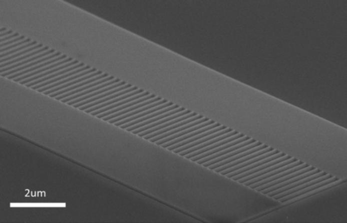
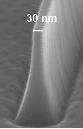
33 Key enabling technology I: RIE by BCl 3 /SiCl 4 /Ar chemistry 28 nm 240 nm Sub-30 nm resolution Aspect ratio > 8 Smooth sidewall and surface Substrate temperature critical during RIE Zhao, EDL
 before after 5 cycles Planar etching rate: ~1 nm/cycle Shrinks NW diameter by 2 nm per cycle Unchanged shape Reduced roughness Lin, EDL")
34 Key enabling technology II: digital etch Self-limiting O 2 plasma oxidation + H 2 SO 4 oxide removal Rate (nm/cycle) Experiment Model Oxidation time (s) before after 5 cycles Planar etching rate: ~1 nm/cycle Shrinks NW diameter by 2 nm per cycle Unchanged shape Reduced roughness Lin, EDL 2014 Zhao, EDL

35 Optimized RIE + Digital Etch 15 nm 240 nm Zhao, EDL 2014 Sub-20 nm resolution Aspect ratio = 16, vertical sidewall Smooth sidewall and surface 35

36 Tomioka, Nature 2012 Persson, DRC 2012 Process flow 36
 0 0.0 0.1 0.2 0.3 0.4 0.5 V ds (V) I d (µa/µm) 200 150 100 50 g m, pk (V ds =0.")
 300 250 200 150 100 50 0 g m (µs/µm) Single nanowire MOSFET: L ch = 80 nm 4.5 nm Al 2 O 3 (EOT = 2.")
37 I d (µa/µm) NW-MOSFET I-V characteristics D=30 nm V gs =-0.6 V to 0.8 V in 0.1 V step R on =759 Ω.µm (at V gs =1 V) V ds (V) I d (µa/µm) g m, pk (V ds =0.5 V) =280 µs/µm V ds =0.5 V V gs (V) g m (µs/µm) Single nanowire MOSFET: L ch = 80 nm 4.5 nm Al 2 O 3 (EOT = 2.2 nm) At V DS =0.5 V: g m,pk =280 μs/μm R on =759 Ω.μm Zhao, IEDM
38 S (mv/dec) g m (µs/µm) Impact of nanowire diameter V ds =0.5 V V ds =0.05 V Diameter (nm) V ds =0.5 V Diameter (nm) DIBL (mv/v) R on (Ω.µm) V gs =1 V Diameter (nm) Diameter (nm) D S, DIBL, g m, R on Error bars indicate distribution of ~10 devices 38
39 Impact of digital etch Single nanowire MOSFET: D= 30 nm (final diameter) Zhao, EDL 2014 Digital etch S, g m Better sidewall interface 39

40 Persson, EDL 2012 g m,pk (µs/µm) Benchmarking Tanaka, APEX 10 Tomioka, IEDM 11 Tomioka, Nature 12 Persson, DRC 12 Persson, EDL 10 This work (Top down) This work V ds =0.5 V S(mV/dec) Bottom up Persson, DRC 2012 Tomioka, Nature 2012 Tanaka, APEX 2010 Trade-off: D S but also g m Top-down approach as good as bottom-up approach 40
41 InGaAs VNW MOSFET Concerns (a short list ) Relatively poor subthreshold behavior S [mv/dec] small V DS DIBL [mv/v] Auth, EDL 1997 L g /λ eff L g /λ eff Electrostatic characteristic length for GAA NW 41
42 InGaAs VNW MOSFET Concerns (a short list ) Excess I off due to BTBT + Floating BJT Quantization enhances bandgap Vertical bandgap engineering InAs NWs Wang, ACSNano
43 InGaAs VNW MOSFET Concerns (a short list ) InGaAs low DOS limits current Increase in injection velocity with carrier density more than compensates for this D=5 nm (?) NW MOSFET Yu, TED

44 InGaAs VNW MOSFET Concerns (a short list ) V T sensitivity to nanowire diameter very tight manufacturing tolerance W f =8 nm Trigate MOSFETs Gray: nanowire array Individual nanowires Agrawal, TED 2013 Teherani, PhD MIT,
45 InGaAs VNW MOSFET Concerns (a short list ) Asymmetric device behavior: D down D up more restrictive circuit wiring I d (µa/µm) V gs = -0.6 to 0.6 V in 0.2 V step D = 40 nm, L g = 80 nm Drain at bottom Drain on top V ds (V) 45
46 InGaAs VNW MOSFET Concerns (a short list ) Sensitivity to few defects 200 V gs =-0.6 V to 0.8 V in 0.1 V step R on =759 Ω.µm (at V gs =1 V) I d (µa/µm) V ds (V) D=7 nm, L g =14 nm (5 nm design rules) S g =540 nm 2 D it =2x10 11 cm -2.eV -1 N it ~1 ev -1 46
47 InGaAs VNW MOSFET Concerns (a short list ) Top contact resistance Difficult to introduce mechanical stress Self-heating 47
48 Conclusions 1. Great recent progress on planar, fin and nanowire III-V MOSFETs 2. Vertical Nanowire III-V MOSFET: superior scalability and power/performance characteristics 3. Vertical Nanowire n- and p-type III-V MOSFET: plausible path for co-integration on Si 4. Many demonstrations of InGaAs VNW MOSFETs by bottom-up and top-down approaches 5. Many issues to work out: sub-10 nm diameter nanowire fabrication, self-aligned contacts, device asymmetry, Introduction of mechanical stress, V T control, device variability, BTBT and parasitic HBT gain, trapping, self-heating, reliability, co-integration with p-type VNW on Si, 48


49 A lot of work ahead but exciting future for III-V electronics 49
Nanoscale III-V CMOS
 Nanoscale III-V CMOS J. A. del Alamo Microsystems Technology Laboratories Massachusetts Institute of Technology SEMI Advanced Semiconductor Manufacturing Conference Saratoga Springs, NY; May 16-19, 2016
III-V Channel Transistors
 III-V Channel Transistors Jesús A. del Alamo Professor Microsystems Technology Laboratories MIT Acknowledgements: Students and collaborators: D. Antoniadis, J. Lin, W. Lu, A. Vardi, X. Zhao Sponsors: Applied
III-V CMOS: Quo Vadis?
 III-V CMOS: Quo Vadis? J. A. del Alamo, X. Cai, W. Lu, A. Vardi, and X. Zhao Microsystems Technology Laboratories Massachusetts Institute of Technology Compound Semiconductor Week 2018 Cambridge, MA, May
InGaAs MOSFET Electronics
 InGaAs MOSFET Electronics J. A. del Alamo Microsystems Technology Laboratories, MIT The 17 th International Symposium Physics of Semiconductors and Applications Jeju, Korea, December 7-11, 2014 Acknowledgements:
Towards Sub-10 nm Diameter InGaAs Vertical nanowire MOSFETs and TFETs
 Towards Sub-10 nm Diameter InGaAs Vertical nanowire MOSFETs and TFETs J. A. del Alamo, X. Zhao, W. Lu, and A. Vardi Microsystems Technology Laboratories Massachusetts Institute of Technology 5 th Berkeley
Vertical Nanowire InGaAs MOSFETs Fabricated by a Top-down Approach
 Vertical Nanowire InGaAs MOSFETs Fabricated by a Top-down Approach Xin Zhao, Jianqiang Lin, Christopher Heidelberger, Eugene A. Fitzgerald and Jesús A. del Alamo Microsystems Technology Laboratories, MIT
III-V Vertical Nanowire FETs with Steep Subthreshold Towards Sub-10 nm Diameter Devices
 III-V Vertical Nanowire FETs with Steep Subthreshold Towards Sub-10 nm Diameter Devices Jesús A. del Alamo, Xin Zhao, Wenjie Lu, Alon Vardi Microsystems Technology Laboratories, MIT E 3 S Retreat September
A New Self-aligned Quantum-Well MOSFET Architecture Fabricated by a Scalable Tight-Pitch Process
 A New Self-aligned Quantum-Well MOSFET Architecture Fabricated by a Scalable Tight-Pitch Process Jianqiang Lin, Xin Zhao, Tao Yu, Dimitri A. Antoniadis, and Jesús A. del Alamo Microsystems Technology Laboratories,
InGaAs MOSFETs for CMOS:
 InGaAs MOSFETs for CMOS: Recent Advances in Process Technology J. A. del Alamo, D. Antoniadis, A. Guo, D.-H. Kim 1, T.-W. Kim 2, J. Lin, W. Lu, A. Vardi and X. Zhao Microsystems Technology Laboratories,
III-V CMOS: the key to sub-10 nm electronics?
 III-V CMOS: the key to sub-10 nm electronics? J. A. del Alamo Microsystems Technology Laboratories, MIT 2011 MRS Spring Meeting and Exhibition Symposium P: Interface Engineering for Post-CMOS Emerging
Nanometer-Scale InGaAs Field-Effect Transistors for THz and CMOS Technologies
 Nanometer-Scale InGaAs Field-Effect Transistors for THz and CMOS Technologies J. A. del Alamo Microsystems Technology Laboratories, MIT ESSDERC-ESSCIRC 2013 Bucharest, Romania, September 16-20, 2013 Acknowledgements:
Sub-30 nm InAs Quantum-Well MOSFETs with Self-Aligned Metal Contacts and Sub-1 nm EOT HfO 2 Insulator
 Sub-30 nm InAs Quantum-Well MOSFETs with Self-Aligned Metal Contacts and Sub-1 nm EOT HfO 2 Insulator Jianqiang Lin, Dimitri A. Antoniadis, and Jesús A. del Alamo Microsystems Technology Laboratories,
Record I on (0.50 ma/μm at V DD = 0.5 V and I off = 100 na/μm) 25 nm-gate-length ZrO 2 /InAs/InAlAs MOSFETs
 25 nm-gate-length ZrO 2 /InAs/InAlAs MOSFETs") Record I on (0.50 ma/μm at V DD = 0.5 V and I off = 100 na/μm) 25 nm-gate-length ZrO 2 /InAs/InAlAs MOSFETs Sanghoon Lee 1*, V. Chobpattana 2,C.-Y. Huang 1, B. J. Thibeault 1, W. Mitchell 1, S. Stemmer
Record I on (0.50 ma/μm at V DD = 0.5 V and I off = 100 na/μm) 25 nm-gate-length ZrO 2 /InAs/InAlAs MOSFETs Sanghoon Lee 1*, V. Chobpattana 2,C.-Y. Huang 1, B. J. Thibeault 1, W. Mitchell 1, S. Stemmer
InGaAs Nanoelectronics: from THz to CMOS
 InGaAs Nanoelectronics: from THz to CMOS J. A. del Alamo Microsystems Technology Laboratories, MIT IEEE International Conference on Electron Devices and Solid-State Circuits Hong Kong, June 3, 2013 Acknowledgements:
InGaAs is a promising channel material candidate for
 468 IEEE TRANSACTIONS ON SEMICONDUCTOR MANUFACTURING, VOL. 30, NO. 4, NOVEMBER 2017 A Si-Compatible Fabrication Process for Scaled Self-Aligned InGaAs FinFETs A. Vardi, Member, IEEE, J.Lin,Member, IEEE,
InAs Quantum-Well MOSFET for logic and microwave applications
 AWAD June 29 th 2012 Accelerating the next technology revolution InAs Quantum-Well MOSFET for logic and microwave applications T.-W. Kim, R. Hill, C. D. Young, D. Veksler, L. Morassi, S. Oktybrshky 1,
Record Extrinsic Transconductance (2.45 ms/μm at V DS = 0.5 V) InAs/In 0.53 Ga 0.47 As Channel MOSFETs Using MOCVD Source-Drain Regrowth
 InAs/In 0.53 Ga 0.47 As Channel MOSFETs Using MOCVD Source-Drain Regrowth") Record Extrinsic Transconductance (2.45 ms/μm at = 0.5 V) InAs/In 0.53 Ga 7 As Channel MOSFETs Using MOCVD Source-Drain Regrowth Sanghoon Lee 1*, C.-Y. Huang 1, A. D. Carter 1, D. C. Elias 1, J. J. M.
Record Extrinsic Transconductance (2.45 ms/μm at = 0.5 V) InAs/In 0.53 Ga 7 As Channel MOSFETs Using MOCVD Source-Drain Regrowth Sanghoon Lee 1*, C.-Y. Huang 1, A. D. Carter 1, D. C. Elias 1, J. J. M.
Zota, Cezar B.; Lindelow, Fredrik; Wernersson, Lars Erik; Lind, Erik
 InGaAs tri-gate MOSFETs with record on-current Zota, Cezar B.; Lindelow, Fredrik; Wernersson, Lars Erik; Lind, Erik Published in: 6 IEEE International Electron Devices Meeting, IEDM 6 DOI:.9/IEDM.6.7886
CMOS beyond Si: Nanometer-Scale III-V MOSFETs
 CMOS beyond Si: Nanometer-Scale III-V MOSFETs Jesús A. del Alamo, Xiaowei Cai, Jianqiang Lin, Wenjie Lu, Alon Vardi, Xin Zhao Microsystems Technology Laboratories, Massachusetts Institute of Technology,
Single suspended InGaAs nanowire MOSFETs
 Single suspended InGaAs nanowire MOSFETs Zota, Cezar B.; Wernersson, Lars-Erik; Lind, Erik Published in: Technical Digest - International Electron Devices Meeting, IEDM DOI:.9/IEDM.5.7988 Published: 6--6
Vertical InAs/GaAsSb/GaSb tunneling field-effect transistor on Si with S = 48 mv/decade and Ion = 10 A/m for Ioff = 1 na/m at VDS = 0.
 Vertical InAs/GaAsSb/GaSb tunneling field-effect transistor on Si with S = 48 mv/decade and Ion = 10 A/m for Ioff = 1 na/m at VDS = 0.3 V Memisevic, E.; Svensson, Johannes; Hellenbrand, Markus; Lind, Erik;
FinFET Devices and Technologies
 FinFET Devices and Technologies Jack C. Lee The University of Texas at Austin NCCAVS PAG Seminar 9/25/14 Material Opportunities for Semiconductors 1 Why FinFETs? Planar MOSFETs cannot scale beyond 22nm
In principle, the high mobilities of InGaAs and
 114Conference report: IEDM part 2 Meeting the challenge of integrating III-Vs with deep submicron silicon High-mobility devices based on indium gallium arsenide (InGaAs) channels could benefit the performance
Scaling of InGaAs MOSFETs into deep-submicron regime (invited)
") Scaling of InGaAs MOSFETs into deep-submicron regime (invited) Y.Q. Wu, J.J. Gu, and P.D. Ye * School of Electrical and Computer Engineering, Purdue University, West Lafayette, IN 47906 * Tel: 765-494-7611,
Scaling of InGaAs MOSFETs into deep-submicron regime (invited) Y.Q. Wu, J.J. Gu, and P.D. Ye * School of Electrical and Computer Engineering, Purdue University, West Lafayette, IN 47906 * Tel: 765-494-7611,
Integration of III-V heterostructure tunnel FETs on Si using Template Assisted Selective Epitaxy (TASE)
") Integration of III-V heterostructure tunnel FETs on Si using Template Assisted Selective Epitaxy (TASE) K. Moselund 1, D. Cutaia 1. M. Borg 1, H. Schmid 1, S. Sant 2, A. Schenk 2 and H. Riel 1 1 IBM Research
Integration of III-V heterostructure tunnel FETs on Si using Template Assisted Selective Epitaxy (TASE) K. Moselund 1, D. Cutaia 1. M. Borg 1, H. Schmid 1, S. Sant 2, A. Schenk 2 and H. Riel 1 1 IBM Research
Device architectures for the 5nm technology node and beyond Nadine Collaert
 Device architectures for the 5nm technology node and beyond Nadine Collaert Distinguished member of technical staff, imec Outline Introduction Beyond FinFET: lateral nanowires and vertical transistors
EECS130 Integrated Circuit Devices
 EECS130 Integrated Circuit Devices Professor Ali Javey 11/6/2007 MOSFETs Lecture 6 BJTs- Lecture 1 Reading Assignment: Chapter 10 More Scalable Device Structures Vertical Scaling is important. For example,
45nm Bulk CMOS Within-Die Variations. Courtesy of C. Spanos (UC Berkeley) Lecture 11. Process-induced Variability I: Random
 Lecture 11. Process-induced Variability I: Random") 45nm Bulk CMOS Within-Die Variations. Courtesy of C. Spanos (UC Berkeley) Lecture 11 Process-induced Variability I: Random Random Variability Sources and Characterization Comparisons of Different MOSFET
45nm Bulk CMOS Within-Die Variations. Courtesy of C. Spanos (UC Berkeley) Lecture 11 Process-induced Variability I: Random Random Variability Sources and Characterization Comparisons of Different MOSFET
Fin-Shaped Field Effect Transistor (FinFET) Min Ku Kim 03/07/2018
 Min Ku Kim 03/07/2018") Fin-Shaped Field Effect Transistor (FinFET) Min Ku Kim 03/07/2018 ECE 658 Sp 2018 Semiconductor Materials and Device Characterizations OUTLINE Background FinFET Future Roadmap Keeping up w/ Moore s Law
Fin-Shaped Field Effect Transistor (FinFET) Min Ku Kim 03/07/2018 ECE 658 Sp 2018 Semiconductor Materials and Device Characterizations OUTLINE Background FinFET Future Roadmap Keeping up w/ Moore s Law
SUPPLEMENTARY INFORMATION
 SUPPLEMENTARY INFORMATION doi:10.1038/nature11293 1. Formation of (111)B polar surface on Si(111) for selective-area growth of InGaAs nanowires on Si. Conventional III-V nanowires (NWs) tend to grow in
Enabling Breakthroughs In Technology
 Enabling Breakthroughs In Technology Mike Mayberry Director of Components Research VP, Technology and Manufacturing Group Intel Corporation June 2011 Defined To be defined Enabling a Steady Technology
Parameter Optimization Of GAA Nano Wire FET Using Taguchi Method
 Parameter Optimization Of GAA Nano Wire FET Using Taguchi Method S.P. Venu Madhava Rao E.V.L.N Rangacharyulu K.Lal Kishore Professor, SNIST Professor, PSMCET Registrar, JNTUH Abstract As the process technology
Drain. Drain. [Intel: bulk-si MOSFETs]
![Drain. Drain. [Intel: bulk-si MOSFETs]](/thumbs/89/97695223.jpg "Drain. Drain. [Intel: bulk-si MOSFETs]") 1 Introduction For more than 40 years, the evolution and growth of very-large-scale integration (VLSI) silicon-based integrated circuits (ICs) have followed from the continual shrinking, or scaling, of
1 Introduction For more than 40 years, the evolution and growth of very-large-scale integration (VLSI) silicon-based integrated circuits (ICs) have followed from the continual shrinking, or scaling, of
EECS130 Integrated Circuit Devices
 EECS130 Integrated Circuit Devices Professor Ali Javey 11/01/2007 MOSFETs Lecture 5 Announcements HW7 set is due now HW8 is assigned, but will not be collected/graded. MOSFET Technology Scaling Technology
Electrical Characterization and Modeling of Gate-Last Vertical InAs Nanowire MOSFETs on Si
 Electrical Characterization and Modeling of Gate-Last Vertical InAs Nanowire MOSFETs on Si Berg, Martin; Kilpi, Olli-Pekka; Persson, Karl-Magnus; Svensson, Johannes; Hellenbrand, Markus; Lind, Erik; Wernersson,
Ultra High-Speed InGaAs Nano-HEMTs
 Ultra High-Speed InGaAs Nano-HEMTs 2003. 10. 14 Kwang-Seok Seo School of Electrical Eng. and Computer Sci. Seoul National Univ., Korea Contents Introduction to InGaAsNano-HEMTs Nano Patterning Process
Self-aligned, gate-last process for vertical InAs nanowire MOSFETs on Si
 Self-aligned, gate-last process for vertical InAs nanowire MOSFETs on Si Berg, Martin; Persson, Karl-Magnus; Kilpi, Olli-Pekka; Svensson, Johannes; Lind, Erik; Wernersson, Lars-Erik Published in: Technical
Nanometer-Scale III-V MOSFETs
 Received 31 January 2016; revised 3 May 2016; accepted 11 May 2016. Date of publication 7 July, 2016; date of current version 23 August 2016. The review of this paper was arranged by Editor P. R. Berger.
Atomic-layer deposition of ultrathin gate dielectrics and Si new functional devices
 Atomic-layer deposition of ultrathin gate dielectrics and Si new functional devices Anri Nakajima Research Center for Nanodevices and Systems, Hiroshima University 1-4-2 Kagamiyama, Higashi-Hiroshima,
Acknowledgments: This work was supported by Air Force HiREV program and the DTRA Basic Research Program.
 Gate Bias and Geometry Dependence of Total-Ionizing-Dose Effects in InGaAs Quantum-Well MOSFETs K. Ni 1, E. X. Zhang 1, R. D. Schrimpf 1, D. M. Fleetwood 1, R. A. Reed 1, M. L. Alles 1, J. Lin 2, and J.
1020 IEEE TRANSACTIONS ON ELECTRON DEVICES, VOL. 63, NO. 3, MARCH 2016
 1020 IEEE TRANSACTIONS ON ELECTRON DEVICES, VOL. 63, NO. 3, MARCH 2016 InGaAs Quantum-Well MOSFET Arrays for Nanometer-Scale Ohmic Contact Characterization J. Lin, Student Member, IEEE, D. A. Antoniadis,
General look back at MESFET processing. General principles of heterostructure use in FETs
 SMA5111 - Compound Semiconductors Lecture 11 - Heterojunction FETs - General HJFETs, HFETs Last items from Lec. 10 Depletion mode vs enhancement mode logic Complementary FET logic (none exists, or is likely
Eigen # Hole s Wavefunctions, E-k and Equi-Energy Contours from a P-FinFET. Lecture 5
 Eigen # Gate Gate Hole s Wavefunctions, E-k and Equi-Energy Contours from a P-FinFET Lecture 5 Thin-Body MOSFET Carrier Transport quantum confinement effects low-field mobility: Orientation and Si Thickness
Lecture 33 - The Short Metal-Oxide-Semiconductor Field-Effect Transistor (cont.) April 30, 2007
 April 30, 2007") 6.720J/3.43J - Integrated Microelectronic Devices - Spring 2007 Lecture 33-1 Lecture 33 - The Short Metal-Oxide-Semiconductor Field-Effect Transistor (cont.) April 30, 2007 Contents: 1. MOSFET scaling
6.720J/3.43J - Integrated Microelectronic Devices - Spring 2007 Lecture 33-1 Lecture 33 - The Short Metal-Oxide-Semiconductor Field-Effect Transistor (cont.) April 30, 2007 Contents: 1. MOSFET scaling
Fully Depleted Devices
 4 Fully Depleted Devices FDSOI and FinFET Bruce Doris, Ali Khakifirooz, Kangguo Cheng, and Terence Hook CONTENTS 4.1 Overview... 71 4.2 Introduction: Challenges of Conventional CMOS Technology...72 4.3
32nm Technology and Beyond
 32nm Technology and Beyond Paolo Gargini Chairman ITRS IEEE Fellow Director of Technology Strategy Intel Fellow ISS Europe 2009 P. Gargini 1 Agenda Equivalent Scaling 45nm Technology summary 32nm Technology
Sub-micron technology IC fabrication process trends SOI technology. Development of CMOS technology. Technology problems due to scaling
 Goodbye Microelectronics Welcome Nanoelectronics Sub-micron technology IC fabrication process trends SOI technology SiGe Tranzistor in 50nm process Virus The thickness of gate oxide= 1.2 nm!!! Today we
3-D Modelling of the Novel Nanoscale Screen-Grid Field Effect Transistor (SGFET)
") 3-D Modelling of the Novel Nanoscale Screen-Grid Field Effect Transistor (SGFET) Pei W. Ding, Kristel Fobelets Department of Electrical Engineering, Imperial College London, U.K. J. E. Velazquez-Perez
3-D Modelling of the Novel Nanoscale Screen-Grid Field Effect Transistor (SGFET) Pei W. Ding, Kristel Fobelets Department of Electrical Engineering, Imperial College London, U.K. J. E. Velazquez-Perez
SEVERAL III-V materials, due to their high electron
 IEEE TRANSACTIONS ON NUCLEAR SCIENCE, VOL. 64, NO. 1, JANUARY 2017 239 Gate Bias and Geometry Dependence of Total-Ionizing-Dose Effects in InGaAs Quantum-Well MOSFETs Kai Ni, Student Member, IEEE, En Xia
Alternatives to standard MOSFETs. What problems are we really trying to solve?
 Alternatives to standard MOSFETs A number of alternative FET schemes have been proposed, with an eye toward scaling up to the 10 nm node. Modifications to the standard MOSFET include: Silicon-in-insulator
FinFET vs. FD-SOI Key Advantages & Disadvantages
 FinFET vs. FD-SOI Key Advantages & Disadvantages Amiad Conley Technical Marketing Manager Process Diagnostics & Control, Applied Materials ChipEx-2014, Apr 2014 1 Moore s Law The number of transistors
Nanometer-scale InGaAs Field-Effect Transistors for THz and CMOS technologies
 Nanometer-scale InGaAs Field-Effect Transistors for THz and CMOS technologies The MIT Faculty has made this article openly available. Please share how this access benefits you. Your story matters. Citation
CMOS Logic Technology IEEE EDS DL
 IIT-bombay, Tutorial CMOS Logic Technology IEEE EDS DL January 24, 2013 IIT-Bombay, Mumbai, India Hiroshi Iwai Frontier Research Center Tokyo Institute of Technology 1 More Moore approach Technology benchmark
DESIGN OF 20 nm FinFET STRUCTURE WITH ROUND FIN CORNERS USING SIDE SURFACE SLOPE VARIATION
 Journal of Electron Devices, Vol. 18, 2013, pp. 1537-1542 JED [ISSN: 1682-3427 ] DESIGN OF 20 nm FinFET STRUCTURE WITH ROUND FIN CORNERS USING SIDE SURFACE SLOPE VARIATION Suman Lata Tripathi and R. A.
Scaling and Beyond for Logic and Memories. Which perspectives?
 September 26 th, 2012 Minatec, Grenoble - France ISCDG 2012, Short Course Scaling and Beyond for Logic and Memories. Which perspectives? Hiroshi Iwai and Barbara de Salvo Frontier Research Center, Tokyo
Session 3: Solid State Devices. Silicon on Insulator
 Session 3: Solid State Devices Silicon on Insulator 1 Outline A B C D E F G H I J 2 Outline Ref: Taurand Ning 3 SOI Technology SOl materials: SIMOX, BESOl, and Smart Cut SIMOX : Synthesis by IMplanted
Transistors for VLSI, for Wireless: A View Forwards Through Fog
 Plenary, Device Research Conference, June 22, 2015, Ohio State Transistors for VLSI, for Wireless: A View Forwards Through Fog Mark Rodwell, UCSB Low-voltage devices P. Long, E. Wilson, S. Mehrotra, M.
Session 10: Solid State Physics MOSFET
 Session 10: Solid State Physics MOSFET 1 Outline A B C D E F G H I J 2 MOSCap MOSFET Metal-Oxide-Semiconductor Field-Effect Transistor: Al (metal) SiO2 (oxide) High k ~0.1 ~5 A SiO2 A n+ n+ p-type Si (bulk)
DUAL MATERIAL PILE GATE APPROACH FOR LOW LEAKAGE FINFET. Sanjay S. Chopade 1*, Dinesh V. Padole 1
 International Journal of Technology (2017) 1: 168-176 ISSN 2086-9614 IJTech 2017 DUAL MATERIAL PILE GATE APPROACH FOR LOW LEAKAGE FINFET Sanjay S. Chopade 1*, Dinesh V. Padole 1 1 Department of Electronics
MSE 410/ECE 340: Electrical Properties of Materials Fall 2016 Micron School of Materials Science and Engineering Boise State University
 MSE 410/ECE 340: Electrical Properties of Materials Fall 2016 Micron School of Materials Science and Engineering Boise State University Practice Final Exam 1 Read the questions carefully Label all figures
MOS Capacitance and Introduction to MOSFETs
 ECE-305: Fall 2016 MOS Capacitance and Introduction to MOSFETs Professor Peter Bermel Electrical and Computer Engineering Purdue University, West Lafayette, IN USA pbermel@purdue.edu 11/4/2016 Pierret,
Advanced PDK and Technologies accessible through ASCENT
 Advanced PDK and Technologies accessible through ASCENT MOS-AK Dresden, Sept. 3, 2018 L. Perniola*, O. Rozeau*, O. Faynot*, T. Poiroux*, P. Roseingrave^ olivier.faynot@cea.fr *Cea-Leti, Grenoble France;
A 90 nm High Volume Manufacturing Logic Technology Featuring Novel 45 nm Gate Length Strained Silicon CMOS Transistors
 A 90 nm High Volume Manufacturing Logic Technology Featuring Novel 45 nm Gate Length Strained Silicon CMOS Transistors T. Ghani, M. Armstrong, C. Auth, M. Bost, P. Charvat, G. Glass, T. Hoffmann*, K. Johnson#,
CMOS Scaling Beyond FinFETs: Nanowires and TFETs
 SEMATECH Symposium June 23, 2011 Tokyo Accelerating the next technology revolution CMOS Scaling Beyond FinFETs: Nanowires and TFETs Chris Hobbs, Wei-Yip Loh, Kerem Akarvardar, Paul Kirsch, and Raj Jammy
High-Performance Si Nanowire FET with a Semi Gate-Around Structure Suitable for Integration
 High-Performance Si Nanowire FET with a Semi Gate-Around Structure Suitable for Integration Soshi Sato 1, Hideyuki Kamimura 1, Hideaki Arai 1, Kuniyuki Kakushima 2, Parhat Ahmet 1, Kenji Ohmori 3, Keisaku
Alternative Channel Materials for MOSFET Scaling Below 10nm
 Alternative Channel Materials for MOSFET Scaling Below 10nm Doug Barlage Electrical Requirements of Channel Mark Johnson Challenges With Material Synthesis Introduction Outline Challenges with scaling
Advanced Digital Integrated Circuits. Lecture 2: Scaling Trends. Announcements. No office hour next Monday. Extra office hour Tuesday 2-3pm
 EE241 - Spring 20 Advanced Digital Integrated Circuits Lecture 2: Scaling Trends and Features of Modern Technologies Announcements No office hour next Monday Extra office hour Tuesday 2-3pm 2 1 Outline
The 3 D Tri Gate transistor is a variant of the FinFET developed at UC Berkeley, and is being used in Intel s 22nmgeneration. microprocessors.
 On May 4, 2011, Intel Corporation announced what it called the most radical shift in semiconductor technology in 50 years. A new 3 dimensional transistor design will enable the production of integrated
Challenges and Innovations in Nano CMOS Transistor Scaling
 Challenges and Innovations in Nano CMOS Transistor Scaling Tahir Ghani Intel Fellow Logic Technology Development October, 2009 Nikkei Presentation 1 Outline Traditional Scaling Traditional Scaling Limiters,
Partially-insulated MOSFET (PiFET) and Its Application to DRAM Cell Transistor
 and Its Application to DRAM Cell Transistor") 30 CHANG WOO OH et al : PARTIALLY-INSULATED MOSFET (PIFET) AND ITS APPLICATION TO DRAM CELL TRANSISTOR Partially-insulated MOSFET (PiFET) and Its Application to DRAM Cell Transistor Chang Woo Oh, Sung
30 CHANG WOO OH et al : PARTIALLY-INSULATED MOSFET (PIFET) AND ITS APPLICATION TO DRAM CELL TRANSISTOR Partially-insulated MOSFET (PiFET) and Its Application to DRAM Cell Transistor Chang Woo Oh, Sung
Performance Analysis of 20 nm Pentagonal and Trapezoidal NanoWire Transistor with Si and Ge Channel
 Performance Analysis of 20 nm Pentagonal and Trapezoidal NanoWire Transistor with Si and Ge Channel SANDEEP SINGH GILL 1, JAIDEV KAUSHIK 2, NAVNEET KAUR 3 Department of Electronics and Communication Engineering
InGaAs channel MOSFET with self-aligned source/drain MBE regrowth technology
 pss-header will be provided by the publisher Review copy not for distribution 0 0 (pss-logo will be inserted here by the publisher) InGaAs channel MOSFET with self-aligned source/drain MBE regrowth technology
Experimentally reported sub-60mv/dec
 Experimentally reported sub-60mv/dec swing in Tunnel FETs? 1 We considered InAs conventional, lateral transistor architectures: GAA nanowire, Fin FETs FETs (Tri gate) UTB,DG SOI Analysis is not directly
III-V on Si for VLSI. 200 mm III-V on Si. Accelerating the next technology revolution. III-V nfet on 200 mm Si
 III-V on Si for VLSI Accelerating the next technology revolution 200 mm III-V on Si III-V nfet on 200 mm Si R. Hill, C. Park, J. Barnett, J. Huang, N. Goel, J. Oh, W.Y. Loh, J. Price, P. Kirsch, P, Majhi,
Normally-Off Operation of AlGaN/GaN Heterojunction Field-Effect Transistor with Clamping Diode
 JOURNAL OF SEMICONDUCTOR TECHNOLOGY AND SCIENCE, VOL.16, NO.2, APRIL, 2016 ISSN(Print) 1598-1657 http://dx.doi.org/10.5573/jsts.2016.16.2.221 ISSN(Online) 2233-4866 Normally-Off Operation of AlGaN/GaN
Scaling of Vertical InAs GaSb Nanowire Tunneling Field-Effect Transistors on Si
 Scaling of Vertical InAs GaSb Nanowire Tunneling Field-Effect Transistors on Si Memisevic, Elvedin; Svensson, Johannes; Hellenbrand, Markus; Lind, Erik; Wernersson, Lars-Erik Published in: IEEE Electron
Source/Drain Parasitic Resistance Role and Electric Coupling Effect in Sub 50 nm MOSFET Design
 Source/Drain Parasitic Resistance Role and Electric Coupling Effect in Sub 50 nm MOSFET Design 9/25/2002 Jun Yuan, Peter M. Zeitzoff*, and Jason C.S. Woo Department of Electrical Engineering University
ECE 5745 Complex Digital ASIC Design Topic 2: CMOS Devices
 ECE 5745 Complex Digital ASIC Design Topic 2: CMOS Devices Christopher Batten School of Electrical and Computer Engineering Cornell University http://www.csl.cornell.edu/courses/ece5950 Simple Transistor
Power, speed and other highlights at IEDM
 98 Conference report: IEDM Power, speed and other highlights at IEDM Mike Cooke rounds up developments reported at December s 2010 IEEE International Electron Devices Meeting (IEDM) in San Francisco. The
A BRIEF STUDY ON CHALLENGES OF MOSFET AND EVOLUTION OF FINFETS
 A BRIEF STUDY ON CHALLENGES OF MOSFET AND EVOLUTION OF FINFETS ABSTRACT J.Shailaja 1, Y.Priya 2 1 ECE Department, Sphoorthy Engineering College (India) 2 ECE,Sphoorthy Engineering College, (India) The
Transistor Scaling in the Innovation Era. Mark Bohr Intel Senior Fellow Logic Technology Development August 15, 2011
 Transistor Scaling in the Innovation Era Mark Bohr Intel Senior Fellow Logic Technology Development August 15, 2011 MOSFET Scaling Device or Circuit Parameter Scaling Factor Device dimension tox, L, W
Performance investigations of novel dual-material gate (DMG) MOSFET with dielectric pockets (DP)
 MOSFET with dielectric pockets (DP)") Science in China Series E: Technological Sciences 2009 SCIENCE IN CHINA PRESS www.scichina.com tech.scichina.com Performance investigations of novel dual-material gate (DMG) MOSFET with dielectric pockets
Science in China Series E: Technological Sciences 2009 SCIENCE IN CHINA PRESS www.scichina.com tech.scichina.com Performance investigations of novel dual-material gate (DMG) MOSFET with dielectric pockets
Power MOSFET Zheng Yang (ERF 3017,
 ECE442 Power Semiconductor Devices and Integrated Circuits Power MOSFET Zheng Yang (ERF 3017, email: yangzhen@uic.edu) Evolution of low-voltage (
Lecture Wrap up. December 13, 2005
 6.012 Microelectronic Devices and Circuits Fall 2005 Lecture 26 1 Lecture 26 6.012 Wrap up December 13, 2005 Contents: 1. 6.012 wrap up Announcements: Final exam TA review session: December 16, 7:30 9:30
Future MOSFET Devices using high-k (TiO 2 ) dielectric
 dielectric") Future MOSFET Devices using high-k (TiO 2 ) dielectric Prerna Guru Jambheshwar University, G.J.U.S. & T., Hisar, Haryana, India, prernaa.29@gmail.com Abstract: In this paper, an 80nm NMOS with high-k (TiO
Future MOSFET Devices using high-k (TiO 2 ) dielectric Prerna Guru Jambheshwar University, G.J.U.S. & T., Hisar, Haryana, India, prernaa.29@gmail.com Abstract: In this paper, an 80nm NMOS with high-k (TiO
GaN power electronics
 GaN power electronics The MIT Faculty has made this article openly available. Please share how this access benefits you. Your story matters. Citation As Published Publisher Lu, Bin, Daniel Piedra, and
Comparative Study of Silicon and Germanium Doping-less Tunnel Field Effect Transistors
 IJSTE - International Journal of Science Technology & Engineering Volume 2 Issue 5 November 2015 ISSN (online): 2349-784X Comparative Study of Silicon and Germanium Doping-less Tunnel Field Effect Transistors
FinFETs have emerged as the solution to short channel
 IEEE TRANSACTIONS ON ELECTRON DEVICES 1 Fin Shape Impact on FinFET Leakage With Application to Multithreshold and Ultralow-Leakage FinFET Design Brad D. Gaynor and Soha Hassoun, Senior Member, IEEE Abstract
Sub-Threshold Region Behavior of Long Channel MOSFET
 Sub-threshold Region - So far, we have discussed the MOSFET behavior in linear region and saturation region - Sub-threshold region is refer to region where Vt is less than Vt - Sub-threshold region reflects
Channel Engineering for Submicron N-Channel MOSFET Based on TCAD Simulation
 Australian Journal of Basic and Applied Sciences, 2(3): 406-411, 2008 ISSN 1991-8178 Channel Engineering for Submicron N-Channel MOSFET Based on TCAD Simulation 1 2 3 R. Muanghlua, N. Vittayakorn and A.
ITRS MOSFET Scaling Trends, Challenges, and Key Technology Innovations
 Workshop on Frontiers of Extreme Computing Santa Cruz, CA October 24, 2005 ITRS MOSFET Scaling Trends, Challenges, and Key Technology Innovations Peter M. Zeitzoff Outline Introduction MOSFET scaling and
Design of Tunnel FET and its Performance characteristics with various materials
 Design of Tunnel FET and its Performance characteristics with various materials 1 G.SANKARAIAH, 2 CH.SATHYANARAYANA 1 PG Student Sreenidhi Institute of Science and Technology, 2 Assistant Professor 1,
Acknowledgements. Curriculum Vitæ. List of Figures. List of Tables. 1 Introduction Si MOSFET Scaling... 2
 Contents Acknowledgements Curriculum Vitæ Abstract List of Figures List of Tables v vi viii xii xviii 1 Introduction 1 1.1 Si MOSFET Scaling......................... 2 2 General MOSFET Scaling Theory 7
420 Intro to VLSI Design
 Dept of Electrical and Computer Engineering 420 Intro to VLSI Design Lecture 0: Course Introduction and Overview Valencia M. Joyner Spring 2005 Getting Started Syllabus About the Instructor Labs, Problem
Wu Lu Department of Electrical and Computer Engineering and Microelectronics Laboratory, University of Illinois, Urbana, Illinois 61801
 Comparative study of self-aligned and nonself-aligned SiGe p-metal oxide semiconductor modulation-doped field effect transistors with nanometer gate lengths Wu Lu Department of Electrical and Computer
FinFET-based Design for Robust Nanoscale SRAM
 FinFET-based Design for Robust Nanoscale SRAM Prof. Tsu-Jae King Liu Dept. of Electrical Engineering and Computer Sciences University of California at Berkeley Acknowledgements Prof. Bora Nikoli Zheng
Fundamentals of III-V Semiconductor MOSFETs
 Serge Oktyabrsky Peide D. Ye Editors Fundamentals of III-V Semiconductor MOSFETs Springer Contents 1 Non-Silicon MOSFET Technology: A Long Time Coming 1 Jerry M. Woodall 1.1 Introduction 1 1.2 Brief and
SoC Technology in the Era of 3-D Tri-Gate Transistors for Low Power, High Performance, and High Density Applications
 SoC Technology in the Era of 3-D Tri-Gate Transistors for Low Power, High Performance, and High Density Applications Vice President, Technology Manufacturing Group Intel Corporation August 2013 Outlines
Vertical Nanowire Gate-All-Around p-type Tunneling Field-Effect Transistor With Si 0.8 Ge 0.2 /Si Heterojunction
 2012 International Conference on Solid-State and Integrated Circuit (ICSIC 2012) IPCSIT vol. 32 (2012) (2012) IACSIT Press, Singapore Vertical Nanowire Gate-All-Around p-type Tunneling Field-Effect Transistor
Performance Comparison of CMOS and Finfet Based Circuits At 45nm Technology Using SPICE
 RESEARCH ARTICLE OPEN ACCESS Performance Comparison of CMOS and Finfet Based Circuits At 45nm Technology Using SPICE Mugdha Sathe*, Dr. Nisha Sarwade** *(Department of Electrical Engineering, VJTI, Mumbai-19)