FinFET Devices and Technologies
|
|
|
- Willa Webster
- 6 years ago
- Views:
Transcription

1 FinFET Devices and Technologies Jack C. Lee The University of Texas at Austin NCCAVS PAG Seminar 9/25/14 Material Opportunities for Semiconductors 1 Why FinFETs? Planar MOSFETs cannot scale beyond 22nm Gate oxide thickness stops scaling Even with thin EOT, one still encounters electrostatic control problem Even with zero oxide thickness and with halo implant, bad current is still quite large Also heavy halo implant leads to band-to-band tunneling current 2 1


2 Why FinFETs? Ultra-thin body SOI devices provide improved electrostatic control A better solution is double-gate type devices! FinFETs 3 4 T. J. King-Liu VLSI


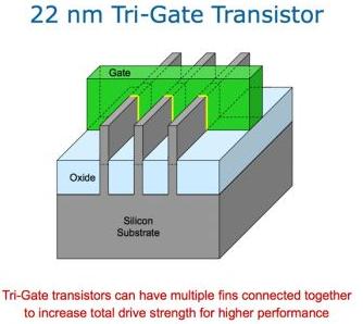
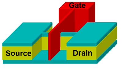
3 5 Tri-Gate Transistor 6 SOURCE: Intel 3


 in order to have good electrostatic control 8 J.")

4 Tri-Gate Transistor 7 Tri-Gate Transistor Scaling H fin and W fin where X UD is lateral diffusion from S/D; W si = W fin W fin is a key parameter for scaling If is too wide, there is no advantage over planar devices W eff must be decreased (along with L eff ) in order to have good electrostatic control 8 J. Kavalieros (Intel) Novel Device Architectures and Material Innovations, VLSI Symposium 2008 Technology Short Course 4


5 T. Hook, IBM, FDSOI Workshop 4/ T. Hook, IBM, FDSOI Workshop 4/2013 5
 ΔH fin might be less for SOI-FinFETs Cost Substrate cost is less for")

6 11 T. Hook, IBM, FDSOI Workshop 4/2013 Bulk-FinFET vs. SOI FinFET Variation of fin heights (ΔH fin ) ΔH fin might be less for SOI-FinFETs Cost Substrate cost is less for bulk-finfets; but processing cost might be less for SOI-FinFETs Heat buildup in channel Bulk FinFETs might be cooler because thermal conductivity is better for Si than SiO 2 Parasitic BJT SOI-FinFETs do not have parasitic BJT problem! lower leakage Epitaxial S/D Might be less difficult for bulk-finfets 12 6

, IEEE TED, Vol. 49, pp.")
7 Self-aligned double patterning (SADP) 13 T. J. King-Liu VLSI 2012 Self-aligned double patterning (SADP) T. J. King-Liu VLSI 2012 & Y.-K. Choi et al. (UC-Berkeley), IEEE TED, Vol. 49, pp ,


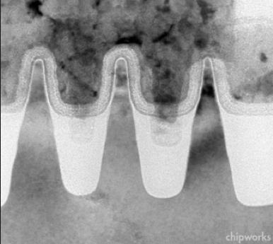
8 Fin fabrication by wet etch Tetramethylammonium hydroxide (TMAH) is a quaternary ammonium salt with the molecular formula N(CH 3 ) 4 + OH -. TMAH is an anisotropic etching of silicon. Etch: 2.38% TMAH solution at 50 C For (111)-oriented sidewall planes, the etch rate is extremely low! Very narrow and straight Si-fin channels can be fabricated 15 Y. X. Liu (Advanced Industrial Science and Technology AIST), IEEE IEDM 2006 Fin fabrication by wet etch 16 Y. X. Liu (Advanced Industrial Science and Technology AIST), IEEE IEDM

9 Bulk-FinFET vs. SOI FinFET Cost Comparison 17 SOURCE: SOI Industry Consortium 18 T. J. King-Liu (UC Berkeley) VLSI Technology


10 Variability -- Bulk-FinFET vs. SOI FinFET 19 SOURCE: SOI Industry Consortium Variability -- Bulk-FinFET vs. SOI FinFET 20 SOURCE: SOI Industry Consortium 10


11 Width quantization W = n x (2 H fin + W fin ) where n = # of fins = quantized = especially bad for analog circuits application which requires various widths 21 Width quantization (cont.) Analog design -- W as a circuit parameter goes from a continuous variable to a set of small positive integers Width quantization changes layout practices (e.g. layout tool to convert gate-width ratios into the necessary number of fins) Layout design rules become more complicated e.g. Spacing rules to reduce coupling SADP adds more complication to layout rules Dummy gate another layout-dependent effect There are already about 5,000 layout rules to check at 20 nm Result is increasing overall design time 22 11

 But fin width is defined by spacer technology. Need various spacer techniques for different widths.")
12 V T control and multiple threshold voltages Particularly important for analog applications How to achieve good threshold control and multiple V T? Traditionally by changing substrate doping concentration N sub and/or by multiple dielectric thicknesses and/or back bias However, for FinFETs or Tri-gate transistors, body is generally undoped. It is also difficult to implement multiple dielectric thicknesses in 3D structures Another way to achieve multiple V T is by using multiple fin widths (i.e. wider fins! higher V T ) But fin width is defined by spacer technology. Need various spacer techniques for different widths. 23 Threshold voltage control and multiple V T schemes V T tuning with aluminum implantation SOI-FinFETs --- Hf-based high-k dielectrics / PVD TiN metal gate Aluminum implant (1E15-1E16/cm 2 ) into TiN metal but not the high-k; using ultralow Trident implanter (3mA at 600eV). Effective work function (EWF) is modulated by Al implantation via Alinduced dipole at the HfO 2 /SiO 2 interface. 24 F. Rao (AMAT & Sematech) Ion Implantation Technology
 or TiCl 4 based ALD-TaN and in-situ CVD-Co/HP-CVD Al as fill-metal (or W as fill metal) Al diffuses differently in/through TiN depending on its growth method Since")

 sidewall planes! better hole mobility (100) sidewall planes! better electron mobility Aggressively scaled W fin leads to more quantization (i.e. QM effects)!")
13 Threshold voltage control and multiple V T schemes V T tuning using aluminum diffusion Interfacial layer SiO 2 by O 3 -oxidation ALD TiN by TDMAT (tetrakis dimethyl amino titanium) or TiCl 4 based ALD-TaN and in-situ CVD-Co/HP-CVD Al as fill-metal (or W as fill metal) Al diffuses differently in/through TiN depending on its growth method Since Al-rich TiN has a more n-type EWF, stacks with higher amount of Al diffused into TiN translate into lower EWF values (i.e. more n-type EWF) Note: TDMAT-TiN is the least Al-rich TiN! Selected for P-MOSFET TiCl 4 -TiN is the most Al-rich TiN! Selected for N-MOSFET 25 A. Veloso (IMEC) VLSI Technology Symposium 2013 Orientation Multiple crystalline planes, depending on the orientation of the fins (i.e. layout) What should the fin direction be patterned? Kuhn SSDM 2009: (110) sidewall planes! better hole mobility (100) sidewall planes! better electron mobility Aggressively scaled W fin leads to more quantization (i.e. QM effects)! mobility decreases Tapered fin results in off-axis planes, causing mobility degradation 26 13


14 27 SOURCE: Intel Temperature Effects of FinFETs FinFETs might suffer worse self-heating effects, especially the so-called SOI-FinFETs


 FDSOI Workshop 2012 3D InGaAs Gate-Wrap-Around FETs Device Structure")
15 Source/drain resistance Merged epitaxy Merged vs. unmerged source/drain regions Merged S/D potentially provide lower source/drain resistance. However, epitaxial growth control can be challenging and may result in increased defect density. Furthermore, stress provided by merged fins for strained-si channel is more difficult to control than unmerged fins 29 T. Hook (IBM) FDSOI Workshop D InGaAs Gate-Wrap-Around FETs Device Structure Top$view " Key features: 50nm undoped In 0.53 Ga 0.47 As channel 1 nm InP barrier layer 7 nm Al 2 O 3 / 60 nm TiN 20 nm N+ layer for Source/Drain F. Xue and J. Lee, IEEE Trans. On Elec. Devices 7/2014 & IEEE IEDM 12/


16 3D InGaAs Gate-Wrap-Around FETs SEM images of InGaAs GWAFETs " Devices with W fin from 40 nm to 200 nm, the gate length of 140 nm and 280 nm, and various numbers of parallel channels were fabricated. F. Xue and J. Lee, IEEE Trans. On Elec. Devices 7/2014 & IEEE IEDM 12/2012 Comparison of Scalability InGaAs FETs GWA W fin =40nm Planar 5nm Channel Planar 10nm Channel DIBL (mv/v) SS (ma/dec) " Better scalability was achieved by GWAFETs compare to planar structure with lower DIBL and SS. " SS is limited by the interface at high-k and InGaAs. F. Xue and J. Lee, IEEE Trans. On Elec. Devices 7/2014 & IEEE IEDM 12/
 have been developed")
17 3D InGaAs Gate-Wrap-Around FETs F. Xue and J. Lee, IEEE Trans. On Elec. Devices 7/2014 & IEEE IEDM 12/2012 Summary FinFETs are needed for 22nm and beyond Fabrication processes of bulk-finfets and SOI-FinFETs using self-aligned double patterning (SADP) have been developed successfully Both bulk-finfets and SOI-FinFETs are in development and production. Both have been compared in terms of process complexity, cost, temperature effects, variability; as well as vertical fins vs. tapered fins (e.g. Structural Stability, Corner Effects, S/D Doping, Mobility) 34 17
18 Summary Width quantization imposes some challenges on circuit design, especially for analog applications Threshold voltage tuning / multiple V T is an important issue, which involves consideration of doped vs. undoped channel, QM effects, asymmetrical t ox, implant/diffused aluminum and cap oxide schemes, gate workfunction control, etc Channel orientation issues: (110) sidewall planes! better hole mobility (100) sidewall planes! better electron mobility Hybrid orientation scheme might be difficult to implement in practice FinFET is applicable to analog circuit and mixed-signal applications 35 18
Fin-Shaped Field Effect Transistor (FinFET) Min Ku Kim 03/07/2018
 Min Ku Kim 03/07/2018") Fin-Shaped Field Effect Transistor (FinFET) Min Ku Kim 03/07/2018 ECE 658 Sp 2018 Semiconductor Materials and Device Characterizations OUTLINE Background FinFET Future Roadmap Keeping up w/ Moore s Law
Fin-Shaped Field Effect Transistor (FinFET) Min Ku Kim 03/07/2018 ECE 658 Sp 2018 Semiconductor Materials and Device Characterizations OUTLINE Background FinFET Future Roadmap Keeping up w/ Moore s Law
45nm Bulk CMOS Within-Die Variations. Courtesy of C. Spanos (UC Berkeley) Lecture 11. Process-induced Variability I: Random
 Lecture 11. Process-induced Variability I: Random") 45nm Bulk CMOS Within-Die Variations. Courtesy of C. Spanos (UC Berkeley) Lecture 11 Process-induced Variability I: Random Random Variability Sources and Characterization Comparisons of Different MOSFET
45nm Bulk CMOS Within-Die Variations. Courtesy of C. Spanos (UC Berkeley) Lecture 11 Process-induced Variability I: Random Random Variability Sources and Characterization Comparisons of Different MOSFET
FinFET-based Design for Robust Nanoscale SRAM
 FinFET-based Design for Robust Nanoscale SRAM Prof. Tsu-Jae King Liu Dept. of Electrical Engineering and Computer Sciences University of California at Berkeley Acknowledgements Prof. Bora Nikoli Zheng
Record I on (0.50 ma/μm at V DD = 0.5 V and I off = 100 na/μm) 25 nm-gate-length ZrO 2 /InAs/InAlAs MOSFETs
 25 nm-gate-length ZrO 2 /InAs/InAlAs MOSFETs") Record I on (0.50 ma/μm at V DD = 0.5 V and I off = 100 na/μm) 25 nm-gate-length ZrO 2 /InAs/InAlAs MOSFETs Sanghoon Lee 1*, V. Chobpattana 2,C.-Y. Huang 1, B. J. Thibeault 1, W. Mitchell 1, S. Stemmer
Record I on (0.50 ma/μm at V DD = 0.5 V and I off = 100 na/μm) 25 nm-gate-length ZrO 2 /InAs/InAlAs MOSFETs Sanghoon Lee 1*, V. Chobpattana 2,C.-Y. Huang 1, B. J. Thibeault 1, W. Mitchell 1, S. Stemmer
ADVANCED MATERIALS AND PROCESSES FOR NANOMETER-SCALE FINFETS
 ADVANCED MATERIALS AND PROCESSES FOR NANOMETER-SCALE FINFETS Tsu-Jae King, Yang-Kyu Choi, Pushkar Ranade^ and Leland Chang Electrical Engineering and Computer Sciences Dept., ^Materials Science and Engineering
FinFET vs. FD-SOI Key Advantages & Disadvantages
 FinFET vs. FD-SOI Key Advantages & Disadvantages Amiad Conley Technical Marketing Manager Process Diagnostics & Control, Applied Materials ChipEx-2014, Apr 2014 1 Moore s Law The number of transistors
Parameter Optimization Of GAA Nano Wire FET Using Taguchi Method
 Parameter Optimization Of GAA Nano Wire FET Using Taguchi Method S.P. Venu Madhava Rao E.V.L.N Rangacharyulu K.Lal Kishore Professor, SNIST Professor, PSMCET Registrar, JNTUH Abstract As the process technology
III-V CMOS: Quo Vadis?
 III-V CMOS: Quo Vadis? J. A. del Alamo, X. Cai, W. Lu, A. Vardi, and X. Zhao Microsystems Technology Laboratories Massachusetts Institute of Technology Compound Semiconductor Week 2018 Cambridge, MA, May
Eigen # Hole s Wavefunctions, E-k and Equi-Energy Contours from a P-FinFET. Lecture 5
 Eigen # Gate Gate Hole s Wavefunctions, E-k and Equi-Energy Contours from a P-FinFET Lecture 5 Thin-Body MOSFET Carrier Transport quantum confinement effects low-field mobility: Orientation and Si Thickness
III-V CMOS: the key to sub-10 nm electronics?
 III-V CMOS: the key to sub-10 nm electronics? J. A. del Alamo Microsystems Technology Laboratories, MIT 2011 MRS Spring Meeting and Exhibition Symposium P: Interface Engineering for Post-CMOS Emerging
EECS130 Integrated Circuit Devices
 EECS130 Integrated Circuit Devices Professor Ali Javey 11/01/2007 MOSFETs Lecture 5 Announcements HW7 set is due now HW8 is assigned, but will not be collected/graded. MOSFET Technology Scaling Technology
Sub-30 nm InAs Quantum-Well MOSFETs with Self-Aligned Metal Contacts and Sub-1 nm EOT HfO 2 Insulator
 Sub-30 nm InAs Quantum-Well MOSFETs with Self-Aligned Metal Contacts and Sub-1 nm EOT HfO 2 Insulator Jianqiang Lin, Dimitri A. Antoniadis, and Jesús A. del Alamo Microsystems Technology Laboratories,
Alternatives to standard MOSFETs. What problems are we really trying to solve?
 Alternatives to standard MOSFETs A number of alternative FET schemes have been proposed, with an eye toward scaling up to the 10 nm node. Modifications to the standard MOSFET include: Silicon-in-insulator
EECS130 Integrated Circuit Devices
 EECS130 Integrated Circuit Devices Professor Ali Javey 11/6/2007 MOSFETs Lecture 6 BJTs- Lecture 1 Reading Assignment: Chapter 10 More Scalable Device Structures Vertical Scaling is important. For example,
ECE 5745 Complex Digital ASIC Design Topic 2: CMOS Devices
 ECE 5745 Complex Digital ASIC Design Topic 2: CMOS Devices Christopher Batten School of Electrical and Computer Engineering Cornell University http://www.csl.cornell.edu/courses/ece5950 Simple Transistor
InGaAs MOSFETs for CMOS:
 InGaAs MOSFETs for CMOS: Recent Advances in Process Technology J. A. del Alamo, D. Antoniadis, A. Guo, D.-H. Kim 1, T.-W. Kim 2, J. Lin, W. Lu, A. Vardi and X. Zhao Microsystems Technology Laboratories,
A New Self-aligned Quantum-Well MOSFET Architecture Fabricated by a Scalable Tight-Pitch Process
 A New Self-aligned Quantum-Well MOSFET Architecture Fabricated by a Scalable Tight-Pitch Process Jianqiang Lin, Xin Zhao, Tao Yu, Dimitri A. Antoniadis, and Jesús A. del Alamo Microsystems Technology Laboratories,
DG-FINFET LOGIC DESIGN USING 32NM TECHNOLOGY
 International Journal of Knowledge Management & e-learning Volume 3 Number 1 January-June 2011 pp. 1-5 DG-FINFET LOGIC DESIGN USING 32NM TECHNOLOGY K. Nagarjuna Reddy 1, K. V. Ramanaiah 2 & K. Sudheer
DESIGN OF 20 nm FinFET STRUCTURE WITH ROUND FIN CORNERS USING SIDE SURFACE SLOPE VARIATION
 Journal of Electron Devices, Vol. 18, 2013, pp. 1537-1542 JED [ISSN: 1682-3427 ] DESIGN OF 20 nm FinFET STRUCTURE WITH ROUND FIN CORNERS USING SIDE SURFACE SLOPE VARIATION Suman Lata Tripathi and R. A.
Fully Depleted Devices
 4 Fully Depleted Devices FDSOI and FinFET Bruce Doris, Ali Khakifirooz, Kangguo Cheng, and Terence Hook CONTENTS 4.1 Overview... 71 4.2 Introduction: Challenges of Conventional CMOS Technology...72 4.3
Lecture 8. Thin-Body MOSFET s Process II. Source/Drain Technologies Threshold Voltage Engineering
 Atom Probe Tomography for Dopants in FinFETs Lecture 8 A.K. Kambham (imec), VLSI-T 2012 Thin-Body MOSFET s Process II Source/Drain Technologies Threshold Voltage Engineering Reading: multiple research
Power MOSFET Zheng Yang (ERF 3017,
 ECE442 Power Semiconductor Devices and Integrated Circuits Power MOSFET Zheng Yang (ERF 3017, email: yangzhen@uic.edu) Evolution of low-voltage (
Lecture 33 - The Short Metal-Oxide-Semiconductor Field-Effect Transistor (cont.) April 30, 2007
 April 30, 2007") 6.720J/3.43J - Integrated Microelectronic Devices - Spring 2007 Lecture 33-1 Lecture 33 - The Short Metal-Oxide-Semiconductor Field-Effect Transistor (cont.) April 30, 2007 Contents: 1. MOSFET scaling
6.720J/3.43J - Integrated Microelectronic Devices - Spring 2007 Lecture 33-1 Lecture 33 - The Short Metal-Oxide-Semiconductor Field-Effect Transistor (cont.) April 30, 2007 Contents: 1. MOSFET scaling
Drain. Drain. [Intel: bulk-si MOSFETs]
![Drain. Drain. [Intel: bulk-si MOSFETs]](/thumbs/89/97695223.jpg "Drain. Drain. [Intel: bulk-si MOSFETs]") 1 Introduction For more than 40 years, the evolution and growth of very-large-scale integration (VLSI) silicon-based integrated circuits (ICs) have followed from the continual shrinking, or scaling, of
1 Introduction For more than 40 years, the evolution and growth of very-large-scale integration (VLSI) silicon-based integrated circuits (ICs) have followed from the continual shrinking, or scaling, of
Enabling Breakthroughs In Technology
 Enabling Breakthroughs In Technology Mike Mayberry Director of Components Research VP, Technology and Manufacturing Group Intel Corporation June 2011 Defined To be defined Enabling a Steady Technology
Design and Analysis of Double Gate MOSFET Devices using High-k Dielectric
 International Journal of Electrical Engineering. ISSN 0974-2158 Volume 7, Number 1 (2014), pp. 53-60 International Research Publication House http://www.irphouse.com Design and Analysis of Double Gate
Atomic-layer deposition of ultrathin gate dielectrics and Si new functional devices
 Atomic-layer deposition of ultrathin gate dielectrics and Si new functional devices Anri Nakajima Research Center for Nanodevices and Systems, Hiroshima University 1-4-2 Kagamiyama, Higashi-Hiroshima,
ITRS MOSFET Scaling Trends, Challenges, and Key Technology Innovations
 Workshop on Frontiers of Extreme Computing Santa Cruz, CA October 24, 2005 ITRS MOSFET Scaling Trends, Challenges, and Key Technology Innovations Peter M. Zeitzoff Outline Introduction MOSFET scaling and
Design of Optimized Digital Logic Circuits Using FinFET
 Design of Optimized Digital Logic Circuits Using FinFET M. MUTHUSELVI muthuselvi.m93@gmail.com J. MENICK JERLINE jerlin30@gmail.com, R. MARIAAMUTHA maria.amutha@gmail.com I. BLESSING MESHACH DASON blessingmeshach@gmail.com.
Session 3: Solid State Devices. Silicon on Insulator
 Session 3: Solid State Devices Silicon on Insulator 1 Outline A B C D E F G H I J 2 Outline Ref: Taurand Ning 3 SOI Technology SOl materials: SIMOX, BESOl, and Smart Cut SIMOX : Synthesis by IMplanted
III-V on Si for VLSI. 200 mm III-V on Si. Accelerating the next technology revolution. III-V nfet on 200 mm Si
 III-V on Si for VLSI Accelerating the next technology revolution 200 mm III-V on Si III-V nfet on 200 mm Si R. Hill, C. Park, J. Barnett, J. Huang, N. Goel, J. Oh, W.Y. Loh, J. Price, P. Kirsch, P, Majhi,
Nanoscale III-V Electronics: from Quantum-Well Planar MOSFETs to Vertical Nanowire MOSFETs
 Nanoscale III-V Electronics: from Quantum-Well Planar MOSFETs to Vertical Nanowire MOSFETs J. A. del Alamo Microsystems Technology Laboratories, MIT Purdue University, West Lafayette, IN; September 29,
2014, IJARCSSE All Rights Reserved Page 1352
 Volume 4, Issue 3, March 2014 ISSN: 2277 128X International Journal of Advanced Research in Computer Science and Software Engineering Research Paper Available online at: www.ijarcsse.com Double Gate N-MOSFET
Innovation to Advance Moore s Law Requires Core Technology Revolution
 Innovation to Advance Moore s Law Requires Core Technology Revolution Klaus Schuegraf, Ph.D. Chief Technology Officer Silicon Systems Group Applied Materials UC Berkeley Seminar March 9 th, 2012 Innovation
Source/Drain Parasitic Resistance Role and Electric Coupling Effect in Sub 50 nm MOSFET Design
 Source/Drain Parasitic Resistance Role and Electric Coupling Effect in Sub 50 nm MOSFET Design 9/25/2002 Jun Yuan, Peter M. Zeitzoff*, and Jason C.S. Woo Department of Electrical Engineering University
Record Extrinsic Transconductance (2.45 ms/μm at V DS = 0.5 V) InAs/In 0.53 Ga 0.47 As Channel MOSFETs Using MOCVD Source-Drain Regrowth
 InAs/In 0.53 Ga 0.47 As Channel MOSFETs Using MOCVD Source-Drain Regrowth") Record Extrinsic Transconductance (2.45 ms/μm at = 0.5 V) InAs/In 0.53 Ga 7 As Channel MOSFETs Using MOCVD Source-Drain Regrowth Sanghoon Lee 1*, C.-Y. Huang 1, A. D. Carter 1, D. C. Elias 1, J. J. M.
Record Extrinsic Transconductance (2.45 ms/μm at = 0.5 V) InAs/In 0.53 Ga 7 As Channel MOSFETs Using MOCVD Source-Drain Regrowth Sanghoon Lee 1*, C.-Y. Huang 1, A. D. Carter 1, D. C. Elias 1, J. J. M.
3-D Modelling of the Novel Nanoscale Screen-Grid Field Effect Transistor (SGFET)
") 3-D Modelling of the Novel Nanoscale Screen-Grid Field Effect Transistor (SGFET) Pei W. Ding, Kristel Fobelets Department of Electrical Engineering, Imperial College London, U.K. J. E. Velazquez-Perez
3-D Modelling of the Novel Nanoscale Screen-Grid Field Effect Transistor (SGFET) Pei W. Ding, Kristel Fobelets Department of Electrical Engineering, Imperial College London, U.K. J. E. Velazquez-Perez
A BRIEF STUDY ON CHALLENGES OF MOSFET AND EVOLUTION OF FINFETS
 A BRIEF STUDY ON CHALLENGES OF MOSFET AND EVOLUTION OF FINFETS ABSTRACT J.Shailaja 1, Y.Priya 2 1 ECE Department, Sphoorthy Engineering College (India) 2 ECE,Sphoorthy Engineering College, (India) The
Scaling of InGaAs MOSFETs into deep-submicron regime (invited)
") Scaling of InGaAs MOSFETs into deep-submicron regime (invited) Y.Q. Wu, J.J. Gu, and P.D. Ye * School of Electrical and Computer Engineering, Purdue University, West Lafayette, IN 47906 * Tel: 765-494-7611,
Scaling of InGaAs MOSFETs into deep-submicron regime (invited) Y.Q. Wu, J.J. Gu, and P.D. Ye * School of Electrical and Computer Engineering, Purdue University, West Lafayette, IN 47906 * Tel: 765-494-7611,
General look back at MESFET processing. General principles of heterostructure use in FETs
 SMA5111 - Compound Semiconductors Lecture 11 - Heterojunction FETs - General HJFETs, HFETs Last items from Lec. 10 Depletion mode vs enhancement mode logic Complementary FET logic (none exists, or is likely
Future MOSFET Devices using high-k (TiO 2 ) dielectric
 dielectric") Future MOSFET Devices using high-k (TiO 2 ) dielectric Prerna Guru Jambheshwar University, G.J.U.S. & T., Hisar, Haryana, India, prernaa.29@gmail.com Abstract: In this paper, an 80nm NMOS with high-k (TiO
Future MOSFET Devices using high-k (TiO 2 ) dielectric Prerna Guru Jambheshwar University, G.J.U.S. & T., Hisar, Haryana, India, prernaa.29@gmail.com Abstract: In this paper, an 80nm NMOS with high-k (TiO
The 3 D Tri Gate transistor is a variant of the FinFET developed at UC Berkeley, and is being used in Intel s 22nmgeneration. microprocessors.
 On May 4, 2011, Intel Corporation announced what it called the most radical shift in semiconductor technology in 50 years. A new 3 dimensional transistor design will enable the production of integrated
Nanoscale III-V CMOS
 Nanoscale III-V CMOS J. A. del Alamo Microsystems Technology Laboratories Massachusetts Institute of Technology SEMI Advanced Semiconductor Manufacturing Conference Saratoga Springs, NY; May 16-19, 2016
32nm Technology and Beyond
 32nm Technology and Beyond Paolo Gargini Chairman ITRS IEEE Fellow Director of Technology Strategy Intel Fellow ISS Europe 2009 P. Gargini 1 Agenda Equivalent Scaling 45nm Technology summary 32nm Technology
Advanced Digital Integrated Circuits. Lecture 2: Scaling Trends. Announcements. No office hour next Monday. Extra office hour Tuesday 2-3pm
 EE241 - Spring 20 Advanced Digital Integrated Circuits Lecture 2: Scaling Trends and Features of Modern Technologies Announcements No office hour next Monday Extra office hour Tuesday 2-3pm 2 1 Outline
Integration of III-V heterostructure tunnel FETs on Si using Template Assisted Selective Epitaxy (TASE)
") Integration of III-V heterostructure tunnel FETs on Si using Template Assisted Selective Epitaxy (TASE) K. Moselund 1, D. Cutaia 1. M. Borg 1, H. Schmid 1, S. Sant 2, A. Schenk 2 and H. Riel 1 1 IBM Research
Integration of III-V heterostructure tunnel FETs on Si using Template Assisted Selective Epitaxy (TASE) K. Moselund 1, D. Cutaia 1. M. Borg 1, H. Schmid 1, S. Sant 2, A. Schenk 2 and H. Riel 1 1 IBM Research
Zota, Cezar B.; Lindelow, Fredrik; Wernersson, Lars Erik; Lind, Erik
 InGaAs tri-gate MOSFETs with record on-current Zota, Cezar B.; Lindelow, Fredrik; Wernersson, Lars Erik; Lind, Erik Published in: 6 IEEE International Electron Devices Meeting, IEDM 6 DOI:.9/IEDM.6.7886
SUPPLEMENTARY INFORMATION
 SUPPLEMENTARY INFORMATION doi:10.1038/nature11293 1. Formation of (111)B polar surface on Si(111) for selective-area growth of InGaAs nanowires on Si. Conventional III-V nanowires (NWs) tend to grow in
Semiconductor TCAD Tools
 Device Design Consideration for Nanoscale MOSFET Using Semiconductor TCAD Tools Teoh Chin Hong and Razali Ismail Department of Microelectronics and Computer Engineering, Universiti Teknologi Malaysia,
2.8 - CMOS TECHNOLOGY
 CMOS Technology (6/7/00) Page 1 2.8 - CMOS TECHNOLOGY INTRODUCTION Objective The objective of this presentation is: 1.) Illustrate the fabrication sequence for a typical MOS transistor 2.) Show the physical
FinFETs have emerged as the solution to short channel
 IEEE TRANSACTIONS ON ELECTRON DEVICES 1 Fin Shape Impact on FinFET Leakage With Application to Multithreshold and Ultralow-Leakage FinFET Design Brad D. Gaynor and Soha Hassoun, Senior Member, IEEE Abstract
EFFECT OF STRUCTURAL AND DOPING PARAMETER VARIATIONS ON NQS DELAY, INTRINSIC GAIN AND NF IN JUNCTIONLESS FETS
 EFFECT OF STRUCTURAL AND DOPING PARAMETER VARIATIONS ON NQS DELAY, INTRINSIC GAIN AND NF IN JUNCTIONLESS FETS B. Lakshmi 1 and R. Srinivasan 2 1 School of Electronics Engineering, VIT University, Chennai,
Final Exam Topics. IC Technology Advancement. Microelectronics Technology in the 21 st Century. Intel s 90 nm CMOS Technology. 14 nm CMOS Transistors
 ANNOUNCEMENTS Final Exam: When: Wednesday 12/10 12:30-3:30PM Where: 10 Evans (last names beginning A-R) 60 Evans (last names beginning S-Z) Comprehensive coverage of course material Closed book; 3 sheets
ISSN: [Soni* et al., 6(4): April, 2017] Impact Factor: 4.116
![ISSN: [Soni* et al., 6(4): April, 2017] Impact Factor: 4.116](/thumbs/94/121304052.jpg "ISSN: [Soni* et al., 6(4): April, 2017] Impact Factor: 4.116") IJESRT INTERNATIONAL JOURNAL OF ENGINEERING SCIENCES & RESEARCH TECHNOLOGY A COMPARITIVELY ANALISIS OF VARIOUS CMOS FINFET STRUCTURE Ragini Soni*, Mrs. Jyotsna Sagar * M.Tech Student (VLSI ) Asst. Professor,
IJESRT INTERNATIONAL JOURNAL OF ENGINEERING SCIENCES & RESEARCH TECHNOLOGY A COMPARITIVELY ANALISIS OF VARIOUS CMOS FINFET STRUCTURE Ragini Soni*, Mrs. Jyotsna Sagar * M.Tech Student (VLSI ) Asst. Professor,
Experimentally reported sub-60mv/dec
 Experimentally reported sub-60mv/dec swing in Tunnel FETs? 1 We considered InAs conventional, lateral transistor architectures: GAA nanowire, Fin FETs FETs (Tri gate) UTB,DG SOI Analysis is not directly
Performance Evaluation of MISISFET- TCAD Simulation
 Performance Evaluation of MISISFET- TCAD Simulation Tarun Chaudhary Gargi Khanna Rajeevan Chandel ABSTRACT A novel device n-misisfet with a dielectric stack instead of the single insulator of n-mosfet
Reduction of Short-Channel Effects in FinFET Mahender Veshala, Ramchander Jatooth, Kota Rajesh Reddy
 Reduction of Short-Channel Effects in FinFET Mahender Veshala, Ramchander Jatooth, Kota Rajesh Reddy Abstract An application of FinFET Technology has opened new development in Nano-technology. Simulations
InGaAs MOSFET Electronics
 InGaAs MOSFET Electronics J. A. del Alamo Microsystems Technology Laboratories, MIT The 17 th International Symposium Physics of Semiconductors and Applications Jeju, Korea, December 7-11, 2014 Acknowledgements:
Channel Engineering for Submicron N-Channel MOSFET Based on TCAD Simulation
 Australian Journal of Basic and Applied Sciences, 2(3): 406-411, 2008 ISSN 1991-8178 Channel Engineering for Submicron N-Channel MOSFET Based on TCAD Simulation 1 2 3 R. Muanghlua, N. Vittayakorn and A.
Session 10: Solid State Physics MOSFET
 Session 10: Solid State Physics MOSFET 1 Outline A B C D E F G H I J 2 MOSCap MOSFET Metal-Oxide-Semiconductor Field-Effect Transistor: Al (metal) SiO2 (oxide) High k ~0.1 ~5 A SiO2 A n+ n+ p-type Si (bulk)
High-Performance Si Nanowire FET with a Semi Gate-Around Structure Suitable for Integration
 High-Performance Si Nanowire FET with a Semi Gate-Around Structure Suitable for Integration Soshi Sato 1, Hideyuki Kamimura 1, Hideaki Arai 1, Kuniyuki Kakushima 2, Parhat Ahmet 1, Kenji Ohmori 3, Keisaku
Low-Power VLSI. Seong-Ook Jung VLSI SYSTEM LAB, YONSEI University School of Electrical & Electronic Engineering
 Low-Power VLSI Seong-Ook Jung 2013. 5. 27. sjung@yonsei.ac.kr VLSI SYSTEM LAB, YONSEI University School of Electrical & Electronic Engineering Contents 1. Introduction 2. Power classification & Power performance
High performance Hetero Gate Schottky Barrier MOSFET
 High performance Hetero Gate Schottky Barrier MOSFET Faisal Bashir *1, Nusrat Parveen 2, M. Tariq Banday 3 1,3 Department of Electronics and Instrumentation, Technology University of Kashmir, Srinagar,
Intel Technology Journal
 Volume 06 Issue 02 Published, May 16, 2002 ISSN 1535766X Intel Technology Journal Semiconductor Technology and Manufacturing Transistor Elements for 30nm Physical Gate Length and Beyond A compiled version
III-V Channel Transistors
 III-V Channel Transistors Jesús A. del Alamo Professor Microsystems Technology Laboratories MIT Acknowledgements: Students and collaborators: D. Antoniadis, J. Lin, W. Lu, A. Vardi, X. Zhao Sponsors: Applied
DUAL MATERIAL PILE GATE APPROACH FOR LOW LEAKAGE FINFET. Sanjay S. Chopade 1*, Dinesh V. Padole 1
 International Journal of Technology (2017) 1: 168-176 ISSN 2086-9614 IJTech 2017 DUAL MATERIAL PILE GATE APPROACH FOR LOW LEAKAGE FINFET Sanjay S. Chopade 1*, Dinesh V. Padole 1 1 Department of Electronics
Performance investigations of novel dual-material gate (DMG) MOSFET with dielectric pockets (DP)
 MOSFET with dielectric pockets (DP)") Science in China Series E: Technological Sciences 2009 SCIENCE IN CHINA PRESS www.scichina.com tech.scichina.com Performance investigations of novel dual-material gate (DMG) MOSFET with dielectric pockets
Science in China Series E: Technological Sciences 2009 SCIENCE IN CHINA PRESS www.scichina.com tech.scichina.com Performance investigations of novel dual-material gate (DMG) MOSFET with dielectric pockets
Challenges and Innovations in Nano CMOS Transistor Scaling
 Challenges and Innovations in Nano CMOS Transistor Scaling Tahir Ghani Intel Fellow Logic Technology Development October, 2009 Nikkei Presentation 1 Outline Traditional Scaling Traditional Scaling Limiters,
International Journal of Scientific & Engineering Research, Volume 6, Issue 2, February-2015 ISSN
 Performance Evaluation and Comparison of Ultra-thin Bulk (UTB), Partially Depleted and Fully Depleted SOI MOSFET using Silvaco TCAD Tool Seema Verma1, Pooja Srivastava2, Juhi Dave3, Mukta Jain4, Priya
Performance advancement of High-K dielectric MOSFET
 Performance advancement of High-K dielectric MOSFET Neha Thapa 1 Lalit Maurya 2 Er. Rajesh Mehra 3 M.E. Student M.E. Student Associate Prof. ECE NITTTR, Chandigarh NITTTR, Chandigarh NITTTR, Chandigarh
y y (12) Patent Application Publication (10) Pub. No.: US 2015/ A1 (19) United States (43) Pub. Date: Sep. 10, C 410C 422b 4200
 Patent Application Publication (10) Pub. No.: US 2015/ A1 (19) United States (43) Pub. Date: Sep. 10, C 410C 422b 4200") (19) United States (12) Patent Application Publication (10) Pub. No.: US 2015/0255300 A1 He et al. US 201502553.00A1 (43) Pub. Date: Sep. 10, 2015 (54) (71) (72) (73) (21) (22) DENSELY SPACED FINS FOR
(19) United States (12) Patent Application Publication (10) Pub. No.: US 2015/0255300 A1 He et al. US 201502553.00A1 (43) Pub. Date: Sep. 10, 2015 (54) (71) (72) (73) (21) (22) DENSELY SPACED FINS FOR
Effect of High-k Gate on the functioning of MOSFET at nano meter sizes
 IOSR Journal of Engineering (IOSRJEN) ISSN (e): 2250-3021, ISSN (p): 2278-8719 Vol. 08, Issue 11 (November. 2018), V (III) PP 49-53 www.iosrjen.org Effect of High-k Gate on the functioning of MOSFET at
Alternative Channel Materials for MOSFET Scaling Below 10nm
 Alternative Channel Materials for MOSFET Scaling Below 10nm Doug Barlage Electrical Requirements of Channel Mark Johnson Challenges With Material Synthesis Introduction Outline Challenges with scaling
Sub-micron technology IC fabrication process trends SOI technology. Development of CMOS technology. Technology problems due to scaling
 Goodbye Microelectronics Welcome Nanoelectronics Sub-micron technology IC fabrication process trends SOI technology SiGe Tranzistor in 50nm process Virus The thickness of gate oxide= 1.2 nm!!! Today we
A Review of Low-Power VLSI Technology Developments
 A Review of Low-Power VLSI Technology Developments Nakka Ravi Kumar Abstract Ever since the invention of integrated circuits, there has been a continuous demand for high-performance, low-power, and low-area/low-cost
Design Simulation and Analysis of NMOS Characteristics for Varying Oxide Thickness
 MIT International Journal of Electronics and Communication Engineering, Vol. 4, No. 2, August 2014, pp. 81 85 81 Design Simulation and Analysis of NMOS Characteristics for Varying Oxide Thickness Alpana
Body-Biased Complementary Logic Implemented Using AlN Piezoelectric MEMS Switches
 University of Pennsylvania From the SelectedWorks of Nipun Sinha 29 Body-Biased Complementary Logic Implemented Using AlN Piezoelectric MEMS Switches Nipun Sinha, University of Pennsylvania Timothy S.
Lecture 020 ECE4430 Review II (1/5/04) Page 020-1
 Page 020-1") Lecture 020 ECE4430 Review II (1/5/04) Page 020-1 LECTURE 020 ECE 4430 REVIEW II (READING: GHLM - Chap. 2) Objective The objective of this presentation is: 1.) Identify the prerequisite material as taught
Lecture 020 ECE4430 Review II (1/5/04) Page 020-1 LECTURE 020 ECE 4430 REVIEW II (READING: GHLM - Chap. 2) Objective The objective of this presentation is: 1.) Identify the prerequisite material as taught
Lecture #29. Moore s Law
 Lecture #29 ANNOUNCEMENTS HW#15 will be for extra credit Quiz #6 (Thursday 5/8) will include MOSFET C-V No late Projects will be accepted after Thursday 5/8 The last Coffee Hour will be held this Thursday
Lecture 020 ECE4430 Review II (1/5/04) Page 020-1
 Page 020-1") Lecture 020 ECE4430 Review II (1/5/04) Page 020-1 LECTURE 020 ECE 4430 REVIEW II (READING: GHLM - Chap. 2) Objective The objective of this presentation is: 1.) Identify the prerequisite material as taught
Lecture 020 ECE4430 Review II (1/5/04) Page 020-1 LECTURE 020 ECE 4430 REVIEW II (READING: GHLM - Chap. 2) Objective The objective of this presentation is: 1.) Identify the prerequisite material as taught
Jack Keil Wolf Lecture. ESE 570: Digital Integrated Circuits and VLSI Fundamentals. Lecture Outline. MOSFET N-Type, P-Type.
 ESE 570: Digital Integrated Circuits and VLSI Fundamentals Jack Keil Wolf Lecture Lec 3: January 24, 2019 MOS Fabrication pt. 2: Design Rules and Layout http://www.ese.upenn.edu/about-ese/events/wolf.php
Vertical Nanowire InGaAs MOSFETs Fabricated by a Top-down Approach
 Vertical Nanowire InGaAs MOSFETs Fabricated by a Top-down Approach Xin Zhao, Jianqiang Lin, Christopher Heidelberger, Eugene A. Fitzgerald and Jesús A. del Alamo Microsystems Technology Laboratories, MIT
Semiconductor Memory: DRAM and SRAM. Department of Electrical and Computer Engineering, National University of Singapore
 Semiconductor Memory: DRAM and SRAM Outline Introduction Random Access Memory (RAM) DRAM SRAM Non-volatile memory UV EPROM EEPROM Flash memory SONOS memory QD memory Introduction Slow memories Magnetic
Performance Analysis of InGaAs Double Gate MOSFET
 Performance Analysis of InGaAs Double Gate MOSFET Ms. Karthika Rani P, Ms. Kavitha T Abstract-Technological improvements have been made due to the scaling of device dimensions in order to attain continuous
Research Needs for Device Sciences Modeling and Simulation (May 6, 2005)
") Research Needs for Device Sciences Modeling and Simulation (May 6, 2005) SRC Device Sciences 2005 Modeling and Simulation Task Force Contributing organizations: Axcelis, Freescale, IBM, Intel, LSI, SRC,
Research Needs for Device Sciences Modeling and Simulation (May 6, 2005) SRC Device Sciences 2005 Modeling and Simulation Task Force Contributing organizations: Axcelis, Freescale, IBM, Intel, LSI, SRC,
Lecture 27 ANNOUNCEMENTS. Regular office hours will end on Monday 12/10 Special office hours will be posted on the EE105 website
 Lecture 27 ANNOUNCEMENTS Regular office hours will end on Monday 12/10 Special office hours will be posted on the EE105 website Final Exam Review Session: Friday 12/14, 3PM, HP Auditorium Video will be
Transistor Scaling in the Innovation Era. Mark Bohr Intel Senior Fellow Logic Technology Development August 15, 2011
 Transistor Scaling in the Innovation Era Mark Bohr Intel Senior Fellow Logic Technology Development August 15, 2011 MOSFET Scaling Device or Circuit Parameter Scaling Factor Device dimension tox, L, W
Performance and Reliability of the sub-100nm FDSOI with High-K K and Metal Gate
 Performance and Reliability of the sub-100nm FDSOI with High-K K and Metal Gate Bich-Yen Nguyen, Anne Vandooren, Aaron Thean, Sriram Kalpat, Melissa Zavala, Jeff Finder, Ted White, Skip Egley, Jamie Schaeffer,
ESE 570: Digital Integrated Circuits and VLSI Fundamentals
 ESE 570: Digital Integrated Circuits and VLSI Fundamentals Lec 3: January 24, 2019 MOS Fabrication pt. 2: Design Rules and Layout Penn ESE 570 Spring 2019 Khanna Jack Keil Wolf Lecture http://www.ese.upenn.edu/about-ese/events/wolf.php
Analog Synaptic Behavior of a Silicon Nitride Memristor
 Supporting Information Analog Synaptic Behavior of a Silicon Nitride Memristor Sungjun Kim, *, Hyungjin Kim, Sungmin Hwang, Min-Hwi Kim, Yao-Feng Chang,, and Byung-Gook Park *, Inter-university Semiconductor
Device architectures for the 5nm technology node and beyond Nadine Collaert
 Device architectures for the 5nm technology node and beyond Nadine Collaert Distinguished member of technical staff, imec Outline Introduction Beyond FinFET: lateral nanowires and vertical transistors
Advanced PDK and Technologies accessible through ASCENT
 Advanced PDK and Technologies accessible through ASCENT MOS-AK Dresden, Sept. 3, 2018 L. Perniola*, O. Rozeau*, O. Faynot*, T. Poiroux*, P. Roseingrave^ olivier.faynot@cea.fr *Cea-Leti, Grenoble France;
In principle, the high mobilities of InGaAs and
 114Conference report: IEDM part 2 Meeting the challenge of integrating III-Vs with deep submicron silicon High-mobility devices based on indium gallium arsenide (InGaAs) channels could benefit the performance
Tunneling Field Effect Transistors for Low Power ULSI
 Tunneling Field Effect Transistors for Low Power ULSI Byung-Gook Park Inter-university Semiconductor Research Center and School of Electrical and Computer Engineering Seoul National University Outline
THRESHOLD VOLTAGE CONTROL SCHEMES
 THRESHOLD VOLTAGE CONTROL SCHEMES IN FINFETS V. Narendar 1, Ramanuj Mishra 2, Sanjeev Rai 3, Nayana R 4 and R. A. Mishra 5 Department of Electronics & Communication Engineering, MNNIT-Allahabad Allahabad-211004,
Optimization of Direct Tunneling Gate Leakage Current in Ultrathin Gate Oxide FET with High-K Dielectrics
 Optimization of Direct Tunneling Gate Leakage Current in Ultrathin Gate Oxide FET with High-K Dielectrics Sweta Chander 1, Pragati Singh 2, S Baishya 3 1,2,3 Department of Electronics & Communication Engineering,
Integrated diodes. The forward voltage drop only slightly depends on the forward current. ELEKTRONIKOS ĮTAISAI
 1 Integrated diodes pn junctions of transistor structures can be used as integrated diodes. The choice of the junction is limited by the considerations of switching speed and breakdown voltage. The forward
Design of Nano-Electro Mechanical (NEM) Relay Based Nano Transistor for Power Efficient VLSI Circuits
 Relay Based Nano Transistor for Power Efficient VLSI Circuits") Design of Nano-Electro Mechanical (NEM) Relay Based Nano Transistor for Power Efficient VLSI Circuits Arul C 1 and Dr. Omkumar S 2 1 Research Scholar, SCSVMV University, Kancheepuram, India. 2 Associate
Design of Nano-Electro Mechanical (NEM) Relay Based Nano Transistor for Power Efficient VLSI Circuits Arul C 1 and Dr. Omkumar S 2 1 Research Scholar, SCSVMV University, Kancheepuram, India. 2 Associate
ECE520 VLSI Design. Lecture 2: Basic MOS Physics. Payman Zarkesh-Ha
 ECE520 VLSI Design Lecture 2: Basic MOS Physics Payman Zarkesh-Ha Office: ECE Bldg. 230B Office hours: Wednesday 2:00-3:00PM or by appointment E-mail: pzarkesh@unm.edu Slide: 1 Review of Last Lecture Semiconductor
Integrated CMOS Tri-Gate Transistors: Paving the Way to Future Technology Generations
 Page 1 Integrated CMOS Tri-Gate Transistors: Paving the Way to Future Technology Generations Robert S. Chau, Intel Senior Fellow Copyright Intel Corporation 2006. *Third-party brands and names are the