Designing Future VLSI Systems with Monolithically Integrated Silicon-Photonics
|
|
|
- Andrea Moore
- 6 years ago
- Views:
Transcription
1 Designing Future VLSI Systems with Monolithically Integrated Silicon-Photonics Vladimir Stojanović University of California, Berkeley SSCS DL Lecture University of Texas, Austin November, 2013
2 2 Acknowledgments Milos Popović (Boulder), Rajeev Ram, Michael Watts, Hanqing Li (MIT), Krste Asanović (UC Berkeley) Jason Orcutt, Jeffrey Shainline, Christopher Batten, Ajay Joshi, Anatoly Khilo Mark Wade, Karan Mehta, Erman Timurdogan, Jie Sun, Cheryl Sorace, Josh Wang Michael Georgas, Jonathan Leu, Benjamin Moss, Chen Sun, Yu-Hsin Chen Yong-Jin Kwon, Scott Beamer, Yunsup Lee, Andrew Waterman, Miquel Planas Roy Meade, Gurtej Sandhu and Fab12 team (Zvi, Ofer, Daniel, Efi, Elad, ) DARPA, Micron, NSF and FCRP IFC IBM Trusted Foundry, CNSE Albany, Solid-State Circuits Society


3 Chip design is going through a change Already have more devices than can use at once Limited by power density and bandwidth Intel Knights Corner 50 cores, 200 Threads Oracle T5 16 cores, 128 Threads Nvidia Fermi 540 CUDA cores IBM Power 7 8 cores, 32 threads Intel 4004 (1971): 4-bit processor, 2312 transistors, ~100 KIPS, 10 micron PMOS, 11 mm 2 chip 1000s of processor cores and accelerators per die The Processor is the new Transistor [Rowen] 3
4 Package pin count 4 Bandwidth, pin count and power scaling 256 cores *> half pins for power supply Need 16k pins in 2017 for HPC* 2,4 cores T5 2 TFlop/s signal 20 Gb/s/link 1 Byte/Flop T5
5 Energy cost [pj/bit] Memory interface scaling problems: Energy-cost and bandwidth density DDR4 GDDR5 Mobile LPDDR Mobile LPDDRX Mobile LPDDRX DDR GB 10 HMC DDR GB LPDDR GDDR5 HMC-Gen1 HMC-Gen Bandwidth density [Gb/s/pin] 5
6 Total memory channel power [W] Power and pins required for 10TFlop/s DDR4 80Tb/s sustained bandwidth assuming 1B/Flop HMC GDDR5 LPDDR Mobile LPDDR Mobile LPDDRX-1666 Mobile LPDDRX 2017 DDR GB DDR GB GDDR5 HMC-Gen1 HMC-Gen # socket pins required for memory channels 6

7 Monolithic Si-Photonics for core-to-core and core-to-dram networks Supercomputers Si-photonics in advanced CMOS and DRAM process NO costly process changes Embedded apps Bandwidth density need dense WDM 7 Energy-efficiency need monolithic integration 7 7
8 Monolithic CMOS photonic integration <150 nm SiO2 Thin BOX SOI CMOS Electronics Bulk CMOS Electronics 8

9 Si and polysi waveguide formation 9 9

10 10 Integrated photonic interconnects Each λ carries one bit of data Bandwidth Density achieved through DWDM Energy-efficiency achieved through low-loss optical components and tight integration


11 Single channel link tradeoffs Loss 10-dB 15-dB Rx Cap 5-fF 25-fF 11


12 Resonance sensitivity Wafer-level ring variation data from our Micron designs Direct thermal tuning Process and temperature shift resonances Direct thermal tuning cost prohibitive Georgas CICC 2011, Sun NOCS


13 Smarter wavelength tuning Georgas CICC 2011, Sun NOCS 2012 Nearest channel tuning + reshuffling Utilize systematic global mismatch and temperature shifts Electrical backend enables dense WDM Helps reduce tuning costs by more than 10x 13


14 Need to optimize carefully 512 Gb/s aggregate throughput Laser energy increases with data-rate Limited Rx sensitivity Modulation more expensive -> lower extinction ratio Tuning costs decrease with data-rate assuming 32nm CMOS Moderate data rates most energy-efficient Georgas CICC
15 DWDM link efficiency optimization Optimize for min energy-cost Bandwidth density dominated by circuit and photonics area (not coupler pitch) 10x better than electrical bump limited 200x better than electrical package pin limit 15


![[Shacham 07]](/docs-images/80/81007692/images/16-2.jpg "[Petracca 08]")
![[Joshi 09]](/docs-images/80/81007692/images/16-3.jpg "[Pan 09]")

![07] [Kirman](/docs-images/80/81007692/images/16-5.jpg "06] [Koka")
16 Many architectural studies show promise 16 [Shacham 07] [Petracca 08] [Joshi 09] [Pan 09] [Vantrease 08] [Psota 07] [Kirman 06] [Koka 08-10] [Batten 08] [Beamer 10]
17 Mem Scheduler Photonic memory interface leveraging optical bandwidth density Laser in MC 1 CPU Super DIMM DRAM cube 1 DRAM cube 4 Important Concepts - Power/message switching (only to active DRAM chip in DRAM cube/super DIMM) MC K Dwr Drd cmd Drd Dwr - Vertical die-to-die coupling (minimizes cabling - 8 dies per DRAM cube) die-die switch cmd ( cube 1, die 8) Dwr Drd ( cube 1, die 1) -Command distributed electrically (broadcast) - Data photonic (single writer multiple readers) Super DIMM K MC 16 Processor die Modulator bank Receiver/PD bank Tunable filterbank DRAM cube 4 Through silicon via Through silicon via hole Enables energy-efficient throughput and capacity scaling per memory channel Beamer ISCA

18 Laser Power Guiding Effectiveness Enables capacity scaling per channel and significant savings in laser energy Beamer ISCA


19 Optimizing DRAM with photonics P1 P4 Floorplan Beamer ISCA

20 Design Space Exploration of Networks Tool DSENT A Tool Connecting Emerging Photonics with Electronics for Opto-Electronic Networks Modeling Chen NOCS 2012 Model Parameters N in N out f clock... Multiplexer Decoder Arbiter Crossbar Buffers DSENT User-Defined Models Router Repeated Link Optical Link Mesh Network Electrical Clos Photonic Clos Area Non-Data- Dependent Power Data-Dependent Energy Technology Parameters Process V DD W min T... Standard Cells Support Models Optical Link Components Technology Characterization Expected Transitions Tools Timing Optimization Optical Link Optimization Delay Available for download at: 20 Kurian IPDPS 2012


21 Significant integration activity, but hybrid and older processes 130nm thick BOX SOI 130nm/90nm thick BOX SOI [Luxtera/Oracle/Kotura] [IBM] [Many schools] [Intel] Bulk CMOS Backend monolithic [HP] [Watts/Sandia/MIT] [Lipson/Cornell] [Kimerling/MIT] 21


22 Our work: Si Electronic-Photonic Integration Timeline Logic Memory MIT-Micron Poly-Si Loss Study (D-1) MIT- Micron Actives Test (D0) DARPA POEM D1S EOS1 EOS2 EOS3 EOS4 EOS EOS12 TI 65nm TI 28nm IBM 9sf IBM 12SOI
 3M Transistors 400 Pads ARM Standard Cells and custom link")
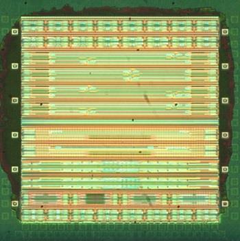
23 EOS Platform: EOS8 fabricated in IBM12SOI 23 Orcutt et al, Optics Express, x 3 mm die 45nm Thin Box SOI Technology (used for Power 7 and Cell processors) 3M Transistors 400 Pads ARM Standard Cells and custom link circuits

24 EOS8 performance summary 24 Fiber-to-chip grating couplers with 3.5 db insertion loss Waveguides under 4dB/cm propagation loss 10 db extinction optical modulators 8 channel wavelength division multiplexing filter bank with <-20 db cross talk All integrated with electronic circuits

 Chip-level verilog")
 Floorplan (macro placement, power grid, routing")


25 Integration of photonics into VLSI tools layout Layout of photonics Layout of Circuit blocks VERSION 5.6 ; BUSBITCHARS "[]" ; DIVIDERCHAR "/" ; modulator.lef MACRO block_electronic_etch_row_1 CLASS BLOCK ; ORIGIN ; abstract abstract LEF LEF LEF of standard cells, I/O pads (provided by ARM) Chip-level verilog (instantiation of.lef macros and connectivity) Floorplan (macro placement, power grid, routing Constraints) SOC Encounter Place and route Place&routed layout FOREIGN block_electronic_etch_row_ ; SIZE 2488 BY 165 ; SYMMETRY X Y R90 ; PIN heater_a_1 DIRECTION INOUT ; USE SIGNAL ; PORT LAYER ua ; Technology files RECT ; END END heater_a_1... OBS LAYER m1 ; RECT ;... END END block_electronic_etch_row_1 END LIBRARY abstract Photonic device p-cell custom photonics-friendly auto-fill 25


 CW laser")
26 Circuit/Device Co-Simulation: VerilogA Driver Circuit Cadence Testbench View Modulator Instantiation Verilog A Model Layout size: 120um x 50um Laser input Inside ring Ring output Optical Eye Diagram Output power (log scale) CW laser frequency increase 26

27 Platform Organization 27


28 Chips fully packaged 28 Fiber Positioner Microscope Fiber Positioner DUT Chip Board HS Clocks Control Board FPGA USB to laptop
29 Best waveguide losses ever reported in a sub-100nm production CMOS line 29 Body-Si waveguides 3-4dB/cm loss Poly waveguides 50dB/cm loss 470nm width 700nm width 700nm width Body-Si ring Q factor 1280nm 1550nm

30 Exceptional dimensional control in 45nm node through drop8 drop7 drop6 drop5 drop4 drop3 drop2 drop1 input 250 GHz spacing > 20 db isolation 30 GHz bandwidth 8-wavelength filterbank results Filter channels fabricated in order Less than 1nm variation Excellent channel isolation (>20dB at 250GHz spacing) 30
 Tuning efficiency 130uW/K (32.")
31 through Integrated thermal tuning circuits drop8 drop7 drop6 drop5 drop4 drop3 drop2 drop1 input integrated digital PWM heater controller tuned as-fabricated 10mW required to retune all 8 rings Negligible overhead of tuning circuits (thermal BW < 500kHz) Tuning efficiency 130uW/K (32.4mW/2π) fully substrate released chips 31


32 Low-power current-sensing optical receiver Georgas ESSCIRC 2011, JSSC 2012 Receiver detects photo current 50fJ/b, ua sensitivities, 3-5Gb/s 32


33 33 Optical modulator design Shainline, Popovic Carrier-injection device at 1550nm Extinction ratio 19dB 45GHz 3dB optical bw at 1280nm Extinction ratio 9dB 60GHz 3dB optical bw

34 Optical modulator electrical tests Carrier-lifetime 2-3ns Diffusion time constant affected by Recombination time Drift conditions 200MHz electrical bandwidth 34


35 Modulator driver sub-bit pre-emphasis 35 Partial forward bias at 0-bit key to fast operation
36 Modulator driver heads Split-supply used for sub-bit pre-emphasis Use core and I/O voltage no regulators 36


37 First modulation in 45nm process 2.5Gb/s modulation 1.2pJ/bit 3dB insertion loss 3dB extinction ratio Moss ISSCC


38 Depletion modulators in 45nm SOI CMOS Shainline et al., Optics Letters


39 Depletion modulators in 45nm SOI CMOS 39 Modulation: 5 Gbps 5.2dB extinction ratio Energy: 55 fj/bit Tunable across FSR with 400GHz/mW (~2nm/mW)
40 Energy cost [pj/bit] Memory interface scaling problems: Energy-cost and bandwidth density DDR4 GDDR5 Mobile LPDDR Mobile LPDDRX-1666 Mobile LPDDRX HMC DDR GB DDR GB GDDR5 HMC-Gen LPDDR POEM PIM HMC-Gen2 POEM Phase 1 POEM Phase 2 POEM Post-phase Bandwidth density [Gb/s/pin] 40
41 Total memory channel power [W] Power and pins required for 10TFlop/s DDR4 80Tb/s sustained bandwidth assuming 1B/Flop GDDR5 Mobile LPDDR Mobile LPDDRX-1666 Mobile LPDDRX 2017 DDR GB 800 HMC DDR GB GDDR POEM PIM LPDDR HMC-Gen1 HMC-Gen2 POEM Phase 1 POEM Phase # socket pins required for memory channels POEM Post-phase 2 41


42 24 mm DRAM side: Bulk integration (polysi photonics) Micron Reticle DTI adjacent to STI Independent Photonics Structures Independent Photonics Structures 4x Integrated Photonics- Electronic Mini-chips 24 mm Independent Photonics Structures DARPA POEM Meade et al Sun et al OI 2013 Data Generators PRB SPRB SPRB SPRB S Tuning Heater Driver = tested Scan I/O 8:2 Serializer DDR Modulator Driver Modulator Device Checkers BER PRB SPRB SPRB SPRB S Heater Driver 2:8 Deserializ er DDR Receive r
43 Summary Silicon-photonics can push both critical dimensions Energy-efficiency monolithic integration Bandwidth Density - dense WDM Need to optimize across layers Connect devices to circuits, and links to networks Building early technology development platforms Feedback to device and circuit designers Accelerated adoption EOS Platform designed for multi-project wafer runs Best end-of-line passives in sub-100nm process (3-4dB/cm loss) sub-100fj/b transmitters/receivers Record-high tuning efficiency with undercut ~ 25uW/K 44

44 Conclusions Silicon-photonics enabler of new capabilities Think new on-chip inductor or new on-chip t-line Potentially revolutionize many applications despite slowdown in CMOS scaling VLSI compute and network infrastructure Wireless comm Imaging and Sensing Need process, device, circuit and system-level understanding So, jump-in and ride the new wave 45
Designing VLSI Interconnects with Monolithically Integrated Silicon-Photonics. Vladimir Stojanović MIT
 Designing VLSI Interconnects with Monolithically Integrated Silicon-Photonics Vladimir Stojanović MIT SSCS DL series Santa Clara, CA, November, 2012 Acknowledgments Rajeev Ram, Henry Smith, Hanqing Li
More-than-Moore with Integrated Silicon-Photonics. Vladimir Stojanović Berkeley Wireless Rearch Center UC Berkeley
 More-than-Moore with Integrated Silicon-Photonics Vladimir Stojanović Berkeley Wireless Rearch Center UC Berkeley 1 Acknowledgments Milos Popović (Boulder/BU), Rajeev Ram, Jason Orcutt, Hanqing Li (MIT),
Silicon photonics and memories
 Silicon photonics and memories Vladimir Stojanović Integrated Systems Group, RLE/MTL MIT Acknowledgments Krste Asanović, Christopher Batten, Ajay Joshi Scott Beamer, Chen Sun, Yon-Jin Kwon, Imran Shamim
Addressing Link-Level Design Tradeoffs for Integrated Photonic Interconnects
 Addressing Link-Level Design Tradeoffs for Integrated Photonic Interconnects Michael Georgas, Jonathan Leu, Benjamin Moss, Chen Sun and Vladimir Stojanović Massachusetts Institute of Technology CICC 2011
Silicon-Photonic Clos Networks for Global On-Chip Communication
 Silicon-Photonic Clos Networks for Global On-Chip Communication Ajay Joshi, Christopher Batten, Yong-Jin Kwon, Scott Beamer, Imran Shamim, Krste Asanović, Vladimir Stojanović NOCS 2009 Massachusetts Institute
Building Manycore Processor-to-DRAM Networks with Monolithic Silicon Photonics
 Building Manycore Processor-to-DRAM Networks with Monolithic Silicon Photonics Christopher Batten 1, Ajay Joshi 1, Jason Orcutt 1, Anatoly Khilo 1 Benjamin Moss 1, Charles Holzwarth 1, Miloš Popović 1,
Lecture: Integration of silicon photonics with electronics. Prepared by Jean-Marc FEDELI CEA-LETI
 Lecture: Integration of silicon photonics with electronics Prepared by Jean-Marc FEDELI CEA-LETI Context The goal is to give optical functionalities to electronics integrated circuit (EIC) The objectives
The Light at the End of the Wire. Dana Vantrease + HP Labs + Mikko Lipasti
 The Light at the End of the Wire Dana Vantrease + HP Labs + Mikko Lipasti 1 Goals of This Talk Why should we (architects) be interested in optics? How does on-chip optics work? What can we build with optics?
NEXT GENERATION SILICON PHOTONICS FOR COMPUTING AND COMMUNICATION PHILIPPE ABSIL
 NEXT GENERATION SILICON PHOTONICS FOR COMPUTING AND COMMUNICATION PHILIPPE ABSIL OUTLINE Introduction Platform Overview Device Library Overview What s Next? Conclusion OUTLINE Introduction Platform Overview
An Example Design using the Analog Photonics Component Library. 3/21/2017 Benjamin Moss
 An Example Design using the Analog Photonics Component Library 3/21/2017 Benjamin Moss Component Library Elements Passive Library Elements: Component Current specs 1 Edge Couplers (Si)
OPTICAL I/O RESEARCH PROGRAM AT IMEC
 OPTICAL I/O RESEARCH PROGRAM AT IMEC IMEC CORE CMOS PHILIPPE ABSIL, PROGRAM DIRECTOR JORIS VAN CAMPENHOUT, PROGRAM MANAGER SCALING TRENDS IN CHIP-LEVEL I/O RECENT EXAMPLES OF HIGH-BANDWIDTH I/O Graphics
A 3.9 ns 8.9 mw 4 4 Silicon Photonic Switch Hybrid-Integrated with CMOS Driver
 A 3.9 ns 8.9 mw 4 4 Silicon Photonic Switch Hybrid-Integrated with CMOS Driver A. Rylyakov, C. Schow, B. Lee, W. Green, J. Van Campenhout, M. Yang, F. Doany, S. Assefa, C. Jahnes, J. Kash, Y. Vlasov IBM
A tunable Si CMOS photonic multiplexer/de-multiplexer
 A tunable Si CMOS photonic multiplexer/de-multiplexer OPTICS EXPRESS Published : 25 Feb 2010 MinJae Jung M.I.C.S Content 1. Introduction 2. CMOS photonic 1x4 Si ring multiplexer Principle of add/drop filter
Monolithic Integra/on of O-band Photonic Transceivers in a Zero-change 32nm SOI CMOS
 Monolithic Integra/on of O-band Photonic Transceivers in a Zero-change 32nm SOI CMOS S. Moazeni 1, A. Atabaki 2, D. Cheian 2, S. Lin 1, R. J. Ram 2, and V. Stojanović 1 1 Department of EECS, University
Building Manycore Processor-to-DRAM Networks with Monolithic Silicon Photonics
 Appears in the Proceedings of the 16th Symposium on High Performance Interconnects (HOTI-16), August 2008 Building Manycore Processor-to-DRAM Networks with Monolithic Silicon Photonics Christopher Batten
Demonstration of an Optical Chip-to-Chip Link in a 3D Integrated Electronic-Photonic Platform
 Demonstration of an Optical Chip-to-Chip Link in a 3D Integrated Electronic-Photonic Platform Sen Lin Krishna Settaluri Sajjad Moazeni Vladimir Stojanovic, Ed. Electrical Engineering and Computer Sciences
EE 232 Lightwave Devices Optical Interconnects
 EE 232 Lightwave Devices Optical Interconnects Sajjad Moazeni Department of Electrical Engineering & Computer Sciences University of California, Berkeley 1 Emergence of Optical Links US IT Map Hyper-Scale
Si Photonics Technology Platform for High Speed Optical Interconnect. Peter De Dobbelaere 9/17/2012
 Si Photonics Technology Platform for High Speed Optical Interconnect Peter De Dobbelaere 9/17/2012 ECOC 2012 - Luxtera Proprietary www.luxtera.com Overview Luxtera: Introduction Silicon Photonics: Introduction
Si photonics for the Zettabyte Era. Marco Romagnoli. CNIT & TeCIP - Scuola Superiore Sant Anna
 Si photonics for the Zettabyte Era Marco Romagnoli CNIT & TeCIP - Scuola Superiore Sant Anna Semicon 2013 Dresden 8-10 October 2013 Zetabyte era Disaggregation at system level Integration at chip level
Silicon Photonics Photo-Detector Announcement. Mario Paniccia Intel Fellow Director, Photonics Technology Lab
 Silicon Photonics Photo-Detector Announcement Mario Paniccia Intel Fellow Director, Photonics Technology Lab Agenda Intel s Silicon Photonics Research 40G Modulator Recap 40G Photodetector Announcement
Addressing Link-Level Design Tradeoffs for Integrated Photonic Interconnects
 Addressing Link-Level Design Tradeoffs for Integrated Photonic Interconnects Michael Georgas, Jonathan Leu, Benjamin Moss, Chen Sun, and Vladimir Stojanović Department of Electrical Engineering and Computer
Optical Bus for Intra and Inter-chip Optical Interconnects
 Optical Bus for Intra and Inter-chip Optical Interconnects Xiaolong Wang Omega Optics Inc., Austin, TX Ray T. Chen University of Texas at Austin, Austin, TX Outline Perspective of Optical Backplane Bus
PROBE: Prediction-based Optical Bandwidth Scaling for Energy-efficient NoCs
 PROBE: Prediction-based Optical Bandwidth Scaling for Energy-efficient NoCs Li Zhou and Avinash Kodi Technologies for Emerging Computer Architecture Laboratory (TEAL) School of Electrical Engineering and
Silicon Optical Modulator
 Silicon Optical Modulator Silicon Optical Photonics Nature Photonics Published online: 30 July 2010 Byung-Min Yu 24 April 2014 High-Speed Circuits & Systems Lab. Dept. of Electrical and Electronic Engineering
Si CMOS Technical Working Group
 Si CMOS Technical Working Group CTR, Spring 2008 meeting Markets Interconnects TWG Breakouts Reception TWG reports Si CMOS: photonic integration E-P synergy - Integration - Standardization - Cross-market
ECE 5745 Complex Digital ASIC Design Topic 2: CMOS Devices
 ECE 5745 Complex Digital ASIC Design Topic 2: CMOS Devices Christopher Batten School of Electrical and Computer Engineering Cornell University http://www.csl.cornell.edu/courses/ece5950 Simple Transistor
TDM Photonic Network using Deposited Materials
 TDM Photonic Network using Deposited Materials ROBERT HENDRY, GILBERT HENDRY, KEREN BERGMAN LIGHTWAVE RESEARCH LAB COLUMBIA UNIVERSITY HPEC 2011 Motivation for Silicon Photonics Performance scaling becoming
IBM T. J. Watson Research Center IBM Corporation
 Broadband Silicon Photonic Switch Integrated with CMOS Drive Electronics B. G. Lee, J. Van Campenhout, A. V. Rylyakov, C. L. Schow, W. M. J. Green, S. Assefa, M. Yang, F. E. Doany, C. V. Jahnes, R. A.
Microphotonics Readiness for Commercial CMOS Manufacturing. Marco Romagnoli
 Microphotonics Readiness for Commercial CMOS Manufacturing Marco Romagnoli MicroPhotonics Consortium meeting MIT, Cambridge October 15 th, 2012 Passive optical structures based on SOI technology Building
Silicon photonics on 3 and 12 μm thick SOI for optical interconnects Timo Aalto VTT Technical Research Centre of Finland
 Silicon photonics on 3 and 12 μm thick SOI for optical interconnects Timo Aalto VTT Technical Research Centre of Finland 5th International Symposium for Optical Interconnect in Data Centres in ECOC, Gothenburg,
Electronic-Photonic ICs for Low Cost and Scalable Datacenter Solutions
 Electronic-Photonic ICs for Low Cost and Scalable Datacenter Solutions Christoph Theiss, Director Packaging Christoph.Theiss@sicoya.com 1 SEMICON Europe 2016, October 27 2016 Sicoya Overview Spin-off from
Silicon photonics with low loss and small polarization dependency. Timo Aalto VTT Technical Research Centre of Finland
 Silicon photonics with low loss and small polarization dependency Timo Aalto VTT Technical Research Centre of Finland EPIC workshop in Tokyo, 9 th November 2017 VTT Technical Research Center of Finland
Silicon Photonics: an Industrial Perspective
 Silicon Photonics: an Industrial Perspective Antonio Fincato Advanced Programs R&D, Cornaredo, Italy OUTLINE 2 Introduction Silicon Photonics Concept 300mm (12 ) Photonic Process Main Silicon Photonics
Signal Integrity Design of TSV-Based 3D IC
 Signal Integrity Design of TSV-Based 3D IC October 24, 21 Joungho Kim at KAIST joungho@ee.kaist.ac.kr http://tera.kaist.ac.kr 1 Contents 1) Driving Forces of TSV based 3D IC 2) Signal Integrity Issues
Opportunities and challenges of silicon photonics based System-In-Package
 Opportunities and challenges of silicon photonics based System-In-Package ECTC 2014 Panel session : Emerging Technologies and Market Trends of Silicon Photonics Speaker : Stéphane Bernabé (Leti Photonics
A high-speed, tunable silicon photonic ring modulator integrated with ultra-efficient active wavelength control
 A high-speed, tunable silicon photonic ring modulator integrated with ultra-efficient active wavelength control Xuezhe Zheng, 1 Eric Chang, 2 Philip Amberg, 1 Ivan Shubin, 1 Jon Lexau, 2 Frankie Liu, 2
APSUNY PDK: Overview and Future Trends
 APSUNY PDK: Overview and Future Trends Erman Timurdogan Analog Photonics, 1 Marina Park Drive, Suite 205, Boston, MA, 02210 erman@analogphotonics.com Silicon Photonics Integrated Circuit Process Design
Silicon Photonics Opportunity, applications & Recent Results
 Silicon Photonics Opportunity, applications & Recent Results Dr. Mario Paniccia Intel Fellow Director, Photonics Technology Lab Intel Corporation www.intel.com/go/sp Purdue University Oct 5 2007 Agenda
Silicon Photonics: A Platform for Integration, Wafer Level Assembly and Packaging
 Silicon Photonics: A Platform for Integration, Wafer Level Assembly and Packaging M. Asghari Kotura Inc April 27 Contents: Who is Kotura Choice of waveguide technology Challenges and merits of Si photonics
HIGH-SPEED LOW-POWER ON-CHIP GLOBAL SIGNALING DESIGN OVERVIEW. Xi Chen, John Wilson, John Poulton, Rizwan Bashirullah, Tom Gray
 HIGH-SPEED LOW-POWER ON-CHIP GLOBAL SIGNALING DESIGN OVERVIEW Xi Chen, John Wilson, John Poulton, Rizwan Bashirullah, Tom Gray Agenda Problems of On-chip Global Signaling Channel Design Considerations
Progress Towards Computer-Aided Design For Complex Photonic Integrated Circuits
 Department of Electrical and Computer Engineering Progress Towards Computer-Aided Design For Complex Photonic Integrated Circuits Wei-Ping Huang Department of Electrical and Computer Engineering McMaster
Signal Integrity Modeling and Measurement of TSV in 3D IC
 Signal Integrity Modeling and Measurement of TSV in 3D IC Joungho Kim KAIST joungho@ee.kaist.ac.kr 1 Contents 1) Introduction 2) 2.5D/3D Architectures with TSV and Interposer 3) Signal integrity, Channel
A Fully Integrated 20 Gb/s Optoelectronic Transceiver Implemented in a Standard
 A Fully Integrated 20 Gb/s Optoelectronic Transceiver Implemented in a Standard 0.13 µm CMOS SOI Technology School of Electrical and Electronic Engineering Yonsei University 이슬아 1. Introduction 2. Architecture
Hot Topics and Cool Ideas in Scaled CMOS Analog Design
 Engineering Insights 2006 Hot Topics and Cool Ideas in Scaled CMOS Analog Design C. Patrick Yue ECE, UCSB October 27, 2006 Slide 1 Our Research Focus High-speed analog and RF circuits Device modeling,
Silicon photonics integration roadmap for applications in computing systems
 Silicon photonics integration roadmap for applications in computing systems Bert Jan Offrein Neuromorphic Devices and Systems Group 2016 IBM Corporation Outline Photonics and computing? The interconnect
ECE 546 Introduction
 ECE 546 Introduction Spring 2018 Jose E. Schutt-Aine Electrical & Computer Engineering University of Illinois jesa@illinois.edu ECE 546 Jose Schutt Aine 1 Future System Needs and Functions Auto Digital
Fully Integrated Switched-Capacitor DC-DC Conversion
 Fully Integrated Switched-Capacitor DC-DC Conversion Elad Alon In collaboration with Hanh-Phuc Le, Seth Sanders Berkeley Wireless Research Center University of California, Berkeley Multi-Core Chips Are
Dynamic Reconfiguration of 3D Photonic Networks-on-Chip for Maximizing Performance and Improving Fault Tolerance
 Dynamic Reconfiguration of 3D Photonic Networks-on-Chip for Maximizing Performance and Improving Fault Tolerance Randy Morris Ϯ, Avinash Kodi Ϯ and Ahmed Louri School of Electrical Engineering and Computer
Fabricating 2.5D, 3D, 5.5D Devices
 Fabricating 2.5D, 3D, 5.5D Devices Bob Patti, CTO rpatti@tezzaron.com Tezzar on Semiconduct or 04/15/2013 1 Gen4 Dis-Integrated 3D Memory DRAM layers 42nm node 2 million vertical connections per lay per
Silicon Photonics Technology Platform To Advance The Development Of Optical Interconnects
 Silicon Photonics Technology Platform To Advance The Development Of Optical Interconnects By Mieke Van Bavel, science editor, imec, Belgium; Joris Van Campenhout, imec, Belgium; Wim Bogaerts, imec s associated
Technology Timeline. Transistors ICs (General) SRAMs & DRAMs Microprocessors SPLDs CPLDs ASICs. FPGAs. The Design Warrior s Guide to.
 SRAMs & DRAMs Microprocessors SPLDs CPLDs ASICs. FPGAs. The Design Warrior s Guide to.") FPGAs 1 CMPE 415 Technology Timeline 1945 1950 1955 1960 1965 1970 1975 1980 1985 1990 1995 2000 Transistors ICs (General) SRAMs & DRAMs Microprocessors SPLDs CPLDs ASICs FPGAs The Design Warrior s Guide
FPGAs 1 CMPE 415 Technology Timeline 1945 1950 1955 1960 1965 1970 1975 1980 1985 1990 1995 2000 Transistors ICs (General) SRAMs & DRAMs Microprocessors SPLDs CPLDs ASICs FPGAs The Design Warrior s Guide
Engineering of Integrated Devices on Electro-Optical Chip: Grating Couplers, Algorithms, and Switches
 Engineering of Integrated Devices on Electro-Optical Chip: Grating Couplers, Algorithms, and Switches by Stevan Lj. Urošević M.Eng. Electrical and Computer Engineering, University of Novi Sad, Faculty
High speed silicon-based optoelectronic devices Delphine Marris-Morini Institut d Electronique Fondamentale, Université Paris Sud
 High speed silicon-based optoelectronic devices Delphine Marris-Morini Institut d Electronique Fondamentale, Université Paris Sud Data centers Optical telecommunications Environment Interconnects Silicon
ECEN689: Special Topics in Optical Interconnects Circuits and Systems Spring 2016
 ECEN689: Special Topics in Optical Interconnects Circuits and Systems Spring 2016 Lecture 1: Introduction Sam Palermo Analog & Mixed-Signal Center Texas A&M University Class Topics System and design issues
EPIC: The Convergence of Electronics & Photonics
 EPIC: The Convergence of Electronics & Photonics K-Y Tu, Y.K. Chen, D.M. Gill, M. Rasras, S.S. Patel, A.E. White ell Laboratories, Lucent Technologies M. Grove, D.C. Carothers, A.T. Pomerene, T. Conway
ISSCC 2006 / SESSION 13 / OPTICAL COMMUNICATION / 13.7
 13.7 A 10Gb/s Photonic Modulator and WDM MUX/DEMUX Integrated with Electronics in 0.13µm SOI CMOS Andrew Huang, Cary Gunn, Guo-Liang Li, Yi Liang, Sina Mirsaidi, Adithyaram Narasimha, Thierry Pinguet Luxtera,
65-GHz Receiver in SiGe BiCMOS Using Monolithic Inductors and Transformers
 65-GHz Receiver in SiGe BiCMOS Using Monolithic Inductors and Transformers Michael Gordon, Terry Yao, Sorin P. Voinigescu University of Toronto March 10 2006, UBC, Vancouver Outline Motivation mm-wave
A Nanophotonic Interconnect for High- Performance Many-Core Computation
 A Nanophotonic Interconnect for High- Performance Many-Core Computation Ray Beausoleil Quantum Optics Research Group Information and Quantum Systems HP Laboratories 008 Hewlett-Packard Development Company,
ECEN689: Special Topics in Optical Interconnects Circuits and Systems Spring 2016
 ECEN689: Special Topics in Optical Interconnects Circuits and Systems Spring 2016 Lecture 10: Electroabsorption Modulator Transmitters Sam Palermo Analog & Mixed-Signal Center Texas A&M University Announcements
Silicon Photonics in Optical Communications. Lars Zimmermann, IHP, Frankfurt (Oder), Germany
, Germany") Silicon Photonics in Optical Communications Lars Zimmermann, IHP, Frankfurt (Oder), Germany Outline IHP who we are Silicon photonics Photonic-electronic integration IHP photonic technology Conclusions
Silicon Photonics in Optical Communications Lars Zimmermann, IHP, Frankfurt (Oder), Germany Outline IHP who we are Silicon photonics Photonic-electronic integration IHP photonic technology Conclusions
ECEN620: Network Theory Broadband Circuit Design Fall 2014
 ECEN620: Network Theory Broadband Circuit Design Fall 2014 Lecture 19: High-Speed Transmitters Sam Palermo Analog & Mixed-Signal Center Texas A&M University Announcements Exam 3 is on Friday Dec 5 Focus
SiGe BiCMOS and Photonic technologies for high frequency and communication applications Andreas Mai
 SiGe BiCMOS and Photonic technologies for high frequency and communication applications Andreas Mai Department Head Technology Outline Introduction & Motivation SiGe HBT device developments for high RF
A 32 Gbps 2048-bit 10GBASE-T Ethernet Energy Efficient LDPC Decoder with Split-Row Threshold Decoding Method
 A 32 Gbps 248-bit GBASE-T Ethernet Energy Efficient LDPC Decoder with Split-Row Threshold Decoding Method Tinoosh Mohsenin and Bevan M. Baas VLSI Computation Lab, ECE Department University of California,
EMT 251 Introduction to IC Design
 EMT 251 Introduction to IC Design (Pengantar Rekabentuk Litar Terkamir) Semester II 2011/2012 Introduction to IC design and Transistor Fundamental Some Keywords! Very-large-scale-integration (VLSI) is
Wafer-scale 3D integration of silicon-on-insulator RF amplifiers
 Wafer-scale integration of silicon-on-insulator RF amplifiers The MIT Faculty has made this article openly available. Please share how this access benefits you. Your story matters. Citation As Published
2009 Spring CS211 Digital Systems & Lab 1 CHAPTER 3: TECHNOLOGY (PART 2)
") 1 CHAPTER 3: IMPLEMENTATION TECHNOLOGY (PART 2) Whatwillwelearninthischapter? we learn in this 2 How transistors operate and form simple switches CMOS logic gates IC technology FPGAs and other PLDs Basic
1 CHAPTER 3: IMPLEMENTATION TECHNOLOGY (PART 2) Whatwillwelearninthischapter? we learn in this 2 How transistors operate and form simple switches CMOS logic gates IC technology FPGAs and other PLDs Basic
On-Chip Optical Interconnects: Prospects and Challenges
 6th International Conference of Soft Computing and Pattern Recognition, August 11-14, 2014, Tunis, Tunisia On-Chip Optical Interconnects: Prospects and Challenges Abderazek Ben Abdallah The University
MICRO RING MODULATOR. Dae-hyun Kwon. High-speed circuits and Systems Laboratory
 MICRO RING MODULATOR Dae-hyun Kwon High-speed circuits and Systems Laboratory Paper preview Title of the paper Low Vpp, ultralow-energy, compact, high-speed silicon electro-optic modulator Publication
Silicon Photonics for Mid-Board Optical Modules Marc Epitaux
 Silicon Photonics for Mid-Board Optical Modules Marc Epitaux Chief Architect at Samtec, Inc Outline Interconnect Solutions Mid-Board Optical Modules Silicon Photonics o Benefits o Challenges DragonFly
Silicon Photonics Transceivers for Hyper Scale Datacenters: Deployment and Roadmap
 Silicon Photonics Transceivers for Hyper Scale Datacenters: Deployment and Roadmap Peter De Dobbelaere Luxtera Inc. 09/19/2016 Luxtera Proprietary www.luxtera.com Luxtera Company Introduction $100B+ Shift
Homework 10 posted just for practice. Office hours next week, schedule TBD. HKN review today. Your feedback is important!
 EE141 Fall 2005 Lecture 26 Memory (Cont.) Perspectives Administrative Stuff Homework 10 posted just for practice No need to turn in Office hours next week, schedule TBD. HKN review today. Your feedback
ON THE WAY TO PHOTONIC INTERPOSERS, BUILDING BLOCKS FOR USR-OPTICAL COMMUNICATION. OPTICS Workshop DATE 2017 Yvain THONNART Mar.
 ON THE WAY TO PHOTONIC INTERPOSERS, BUILDING BLOCKS FOR USR-OPTICAL COMMUNICATION OUTLINE Motivations Interposer technologies for manycores Our goal An optically interconnected manycore on interposer Silicon
MODELING AND EVALUATION OF CHIP-TO-CHIP SCALE SILICON PHOTONIC NETWORKS
 1 MODELING AND EVALUATION OF CHIP-TO-CHIP SCALE SILICON PHOTONIC NETWORKS Robert Hendry, Dessislava Nikolova, Sébastien Rumley, Keren Bergman Columbia University HOTI 2014 2 Chip-to-chip optical networks
Putting PICs in Products A Practical Guideline. Katarzyna Ławniczuk
 Putting PICs in Products A Practical Guideline Katarzyna Ławniczuk k.lawniczuk@brightphotonics.eu Outline Product development considerations Selecting PIC technology Design flow and design tooling considerations
New Wave SiP solution for Power
 New Wave SiP solution for Power Vincent Lin Corporate R&D ASE Group APEC March 7 th, 2018 in San Antonio, Texas. 0 Outline Challenges Facing Human Society Energy, Environment and Traffic Autonomous Driving
Chapter 7 Introduction to 3D Integration Technology using TSV
 Chapter 7 Introduction to 3D Integration Technology using TSV Jin-Fu Li Department of Electrical Engineering National Central University Jungli, Taiwan Outline Why 3D Integration An Exemplary TSV Process
LUCEDA PHOTONICS DELIVERS A SILICON PHOTONICS IC SOLUTION IN TANNER L-EDIT
 LUCEDA PHOTONICS DELIVERS A SILICON PHOTONICS IC SOLUTION IN TANNER L-EDIT WIM BOGAERTS, PIETER DUMON, AND MARTIN FIERS, LUCEDA PHOTONICS JEFF MILLER, MENTOR GRAPHICS A M S D E S I G N & V E R I F I C
Zukunftstechnologie Dünnglasbasierte elektrooptische. Research Center of Microperipheric Technologies
 Zukunftstechnologie Dünnglasbasierte elektrooptische Baugruppenträger Dr. Henning Schröder Fraunhofer IZM, Berlin, Germany Today/Overview Motivation: external roadmaps High Bandwidth and Channel Density
Integration of Optoelectronic and RF Devices for Applications in Optical Interconnect and Wireless Communication
 Integration of Optoelectronic and RF Devices for Applications in Optical Interconnect and Wireless Communication Zhaoran (Rena) Huang Assistant Professor Department of Electrical, Computer and System Engineering
OPTICAL NETWORKS. Building Blocks. A. Gençata İTÜ, Dept. Computer Engineering 2005
 OPTICAL NETWORKS Building Blocks A. Gençata İTÜ, Dept. Computer Engineering 2005 Introduction An introduction to WDM devices. optical fiber optical couplers optical receivers optical filters optical amplifiers
IEEE JOURNAL OF SELECTED TOPICS IN QUANTUM ELECTRONICS 2010 Silicon Photonic Circuits: On-CMOS Integration, Fiber Optical Coupling, and Packaging
 IEEE JOURNAL OF SELECTED TOPICS IN QUANTUM ELECTRONICS 2010 Silicon Photonic Circuits: On-CMOS Integration, Fiber Optical Coupling, and Packaging Christophe Kopp, St ephane Bernab e, Badhise Ben Bakir,
Lecture #29. Moore s Law
 Lecture #29 ANNOUNCEMENTS HW#15 will be for extra credit Quiz #6 (Thursday 5/8) will include MOSFET C-V No late Projects will be accepted after Thursday 5/8 The last Coffee Hour will be held this Thursday
Photo-Electronic Crossbar Switching Network for Multiprocessor Systems
 Photo-Electronic Crossbar Switching Network for Multiprocessor Systems Atsushi Iwata, 1 Takeshi Doi, 1 Makoto Nagata, 1 Shin Yokoyama 2 and Masataka Hirose 1,2 1 Department of Physical Electronics Engineering
Market and technology trends in advanced packaging
 Close Market and technology trends in advanced packaging Executive OVERVIEW Recent advances in device miniaturization trends have placed stringent requirements for all aspects of product manufacturing.
Lecture Perspectives. Administrivia
 Lecture 29-30 Perspectives Administrivia Final on Friday May 18 12:30-3:30 pm» Location: 251 Hearst Gym Topics all what was covered in class. Review Session Time and Location TBA Lab and hw scores to be
Challenges for On-chip Optical Interconnect
 Initial Results of Prototyping a 3-D Integrated Intra-Chip Free-Space Optical Interconnect Berkehan Ciftcioglu, Rebecca Berman, Jian Zhang, Zach Darling, Alok Garg, Jianyun Hu, Manish Jain, Peng Liu, Ioannis
MTO Technology Programs Progress. Frank Stroili Technical Director, RF/Mixed signal
 MTO Technology Programs Progress Frank Stroili Technical Director, RF/Mixed signal 603-885-7487 frank.stroili@baesystems.com 1 Report Documentation Page Form Approved OMB No. 0704-0188 Public reporting
Deep Trench Capacitors for Switched Capacitor Voltage Converters
 Deep Trench Capacitors for Switched Capacitor Voltage Converters Jae-sun Seo, Albert Young, Robert Montoye, Leland Chang IBM T. J. Watson Research Center 3 rd International Workshop for Power Supply on
Integrated Photonics using the POET Optical InterposerTM Platform
 Integrated Photonics using the POET Optical InterposerTM Platform Dr. Suresh Venkatesan CIOE Conference Shenzhen, China Sept. 5, 2018 POET Technologies Inc. TSXV: PUBLIC POET PTK.V Technologies Inc. PUBLIC
Lecture 30. Perspectives. Digital Integrated Circuits Perspectives
 Lecture 30 Perspectives Administrivia Final on Friday December 15 8 am Location: 251 Hearst Gym Topics all what was covered in class. Precise reading information will be posted on the web-site Review Session
+1 (479)
") Introduction to VLSI Design http://csce.uark.edu +1 (479) 575-6043 yrpeng@uark.edu Invention of the Transistor Vacuum tubes ruled in first half of 20th century Large, expensive, power-hungry, unreliable
Introduction to VLSI Design http://csce.uark.edu +1 (479) 575-6043 yrpeng@uark.edu Invention of the Transistor Vacuum tubes ruled in first half of 20th century Large, expensive, power-hungry, unreliable
SUBSTRATE NOISE FULL-CHIP LEVEL ANALYSIS FLOW FROM EARLY DESIGN STAGES TILL TAPEOUT. Hagay Guterman, CSR Jerome Toublanc, Ansys
 SUBSTRATE NOISE FULL-CHIP LEVEL ANALYSIS FLOW FROM EARLY DESIGN STAGES TILL TAPEOUT Hagay Guterman, CSR Jerome Toublanc, Ansys Speakers Hagay Guterman, CSR Hagay Guterman is a senior signal and power integrity
Photonic Integrated Beamformer for Broadband Radio Astronomy
 M. Burla, D. A. I. Marpaung, M. R. H. Khan, C. G. H. Roeloffzen Telecommunication Engineering group University of Twente, Enschede, The Netherlands P. Maat, K. Dijkstra ASTRON, Dwingeloo, The Netherlands
Design Space Exploration of Optical Interfaces for Silicon Photonic Interconnects
 Design Space Exploration of Optical Interfaces for Silicon Photonic Interconnects Olivier Sentieys, Johanna Sepúlveda, Sébastien Le Beux, Jiating Luo, Cedric Killian, Daniel Chillet, Ian O Connor, Hui
Overview of short-reach optical interconnects: from VCSELs to silicon nanophotonics
 Acknowledgements: J. Cunningham, R. Ho, X. Zheng, J. Lexau, H. Thacker, J. Yao, Y. Luo, G. Li, I. Shubin, F. Liu, D. Patil, K. Raj, and J. Mitchell M. Asghari T. Pinguet Overview
ECEN689: Special Topics in Optical Interconnects Circuits and Systems Spring 2016
 ECEN689: Special Topics in Optical Interconnects Circuits and Systems Spring 2016 Lecture 9: Mach-Zehnder Modulator Transmitters Sam Palermo Analog & Mixed-Signal Center Texas A&M University Mach-Zehnder
Integrated electro-optical waveguide based devices with liquid crystals on a silicon backplane
 Integrated electro-optical waveguide based devices with liquid crystals on a silicon backplane Florenta Costache Group manager Smart Micro-Optics SMO/AMS Fraunhofer Institute for Photonic Microsystems,
Lecture 6 Fiber Optical Communication Lecture 6, Slide 1
 Lecture 6 Optical transmitters Photon processes in light matter interaction Lasers Lasing conditions The rate equations CW operation Modulation response Noise Light emitting diodes (LED) Power Modulation
Optical Integrated Devices in Silicon On Insulator for VLSI Photonics
 Optical Integrated Devices in Silicon On Insulator for VLSI Photonics Design, Modelling, Fabrication & Characterization Piero Orlandi 1 Possible Approaches Reduced Design time Transparent Technology Shared
Convergence Challenges of Photonics with Electronics
 Convergence Challenges of Photonics with Electronics Edward Palen, Ph.D., P.E. PalenSolutions - Optoelectronic Packaging Consulting www.palensolutions.com palensolutions@earthlink.net 415-850-8166 October