Silicon photonics and memories
|
|
|
- Sydney Stewart
- 6 years ago
- Views:
Transcription
1 Silicon photonics and memories Vladimir Stojanović Integrated Systems Group, RLE/MTL MIT
2 Acknowledgments Krste Asanović, Christopher Batten, Ajay Joshi Scott Beamer, Chen Sun, Yon-Jin Kwon, Imran Shamim Rajeev Ram, Milos Popovic, Franz Kaertner, Judy Hoyt, Henry Smith, Erich Ippen Hanqin Li, Charles Holzwarth Jason Orcutt, Anatoly Khilo, Jie Sun, Cheryl Sorace, Eugen Zgraggen Michael Georgas, Jonathan Leu, Ben Moss Dr. Jag Shah DARPA MTO Texas Instruments Intel Corporation 2

 - 4-way SIMD")


3 Processors scaling to manycore systems 64-tile system ( cores) - 4-way SIMD GHz TFlops on one chip - Need 5-10 TB/s of off-chip I/O - Even larger bisection bandwidth 2 cm Intel 48 core -Xeon 2 cm 3
4 Bandwidth, pin count and power scaling 8 5GHz 2,4 cores 256 cores Package pin count Need 16k signal pins in 2017 for HPC 2 TFlop/s signal pins 1 Byte/Flop 4
5 Electrical Baseline in 2016 Node Board 10 TFlop/s 512 GB 80 Tb/s mem BW CPU Power 1kW -> 100W Energy-efficiency 100 pj/flop -> 10pJ/Flop 200 W Cross-chip Processor + Router P R DIMM DIMM DIMM DIMM Request DIMM DIMM DIMM DIMM P P P P P P P P P P P P CPU 64 x 8 x 32 = 16k High-speed signal pins DIMM DIMM DIMM DIMM W I/O P P P P 1kW Compute Memory Power 1kW 200 W Cross-chip 400 W I/O 400 W Activate P Processor Router Memory Controller DIMM DIMM DIMM DIMM Response 512 x 1GB chips 8 chips per DIMM 1DIMM per memory channel Need at least 16 banks/chip to sustain BW 64 memory channels (controllers) 1.28 Tb/s per controller 160 Gb/s per chip (16 x 10 5pJ/b 5

6 Monolithic CMOS-Photonics in Computer Systems Supercomputers Si-photonics in advanced bulk CMOS, thin BOX SOI and process NO costly process changes Embedded apps Bandwidth density need dense WDM Energy-efficiency need monolithic integration 6
7 CMOS photonics density and energy advantage Metric Energy (pj/b) Bandwidth density (Gb/s/μ) Global on-chip photonic link Global on-chip optimally repeated electrical link 1 5 Off-chip photonic link (100 μ coupler pitch) Off-chip electrical SERDES (100 μ pitch) Assuming Gb/s wavelengths on each waveguide 7


8 But, need to keep links fully utilized Fixed and static energy increase at low link utilization! Energy [fj/b] 8 8


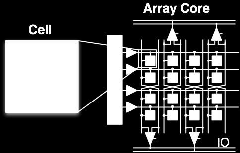
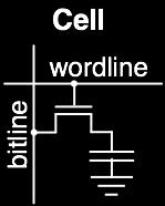
9 Core-to-Memory network: Electrical baseline C = Core, DM = Module Mesh Router Router and Access Point Both cross-chip and I/O costly 9


10 Aggregation with Optical LMGS* network * Local Meshes to Global Switches Ci = Core in Group i, DM = Module, S = Crossbar switch Shorten cross-chip electrical Photonic both part cross-chip and off-chip 10
11 Photonic LMGS: Physical Mapping Network layout optimization significantly affects the component requirements 64-tile system w/ 16 groups, 16 Modules, 320 Gbps bi-di tile- module BW [Joshi et al PICA 2009] 11

12 Photonic LMGS - U-shape 64-tile system w/ 16 groups, 16 Modules, 320 Gbps bi-di tile- module BW 12
13 Photonic LMGS - U-shape 64-tile system w/ 16 groups, 16 Modules, 320 Gbps bi-di tile- module BW 13
14 Photonic LMGS - U-shape 64-tile system w/ 16 groups, 16 Modules, 320 Gbps bi-di tile- module BW 14
15 Photonic LMGS - U-shape 64 tiles 64 waveguides (for tile throughput = 128 b/cyc) 256 modulators per group 256 ring filters per group Total rings > 16K 0.32W (thermal tuning) 15
16 Photonic device requirements in LMGS - U-shape Through loss (db/ring) Waveguide loss (db/cm) Optical Laser Power Die Area Overhead Waveguide loss and Through loss limits for 2 W optical laser power 16

17 Photonic LMGS ring matrix vs u-shape LMGS ring matrix LMGS u-shape 0.64 W power for thermal tuning circuits 2 W optical laser power Waveguide loss < 0.2 db/cm Through loss < db/ring 0.32 W power for thermal tuning circuits 2 W optical laser power Waveguide loss < 1.5 db/cm Through loss < 0.02 db/ring [Batten et al Micro 2009] [Joshi et al PICA 2009] 17


18 Power-bandwidth tradeoff 2-3x better 8-10x better 1 group, OPF = 1 4 group, OPF = 1 16 group, OPF = 1 1 group, OPF = 4 4 group, OPF = 2 16 group, OPF = 1 Electrical with grouping Electrical with grouping and over-provisioning Optical with grouping and over-provisioning 18

![et al ICS 2009] Example](/docs-images/77/75105680/images/19-1.jpg "256 core node with 64")
19 System Organization Defragmentation [Beamer et al ICS 2009] Example 256 core node with 64 core dies 19

20 System Organization Die view 64 core die supporting 256 core node 20
21 Electrical is also Limited Pin-bandwidth on the compute chip I/O energy to move between chips Cross-chip energy within chip Activation energy within chip 21
![Solution: Silicon Photonics [Beamer et al ISCA 2010] Great bandwidth density Great off-chip energy](/docs-images/77/75105680/images/22-0.jpg "efficiency Costs little additional energy to use on-chip after off-chip Enables page size reduction")
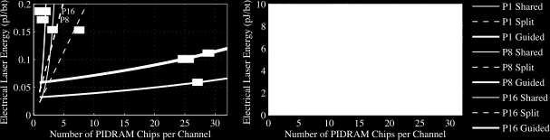
22 Solution: Silicon Photonics [Beamer et al ISCA 2010] Great bandwidth density Great off-chip energy efficiency Costs little additional energy to use on-chip after off-chip Enables page size reduction 22

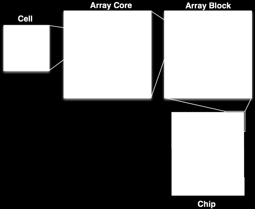
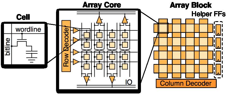
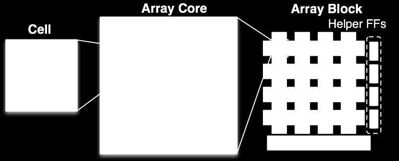
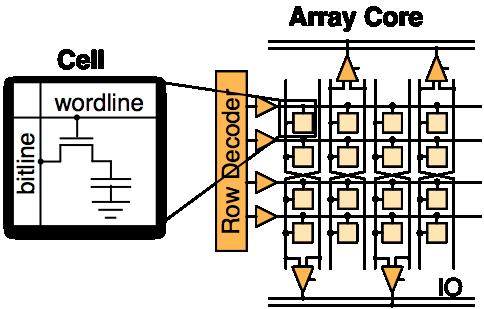
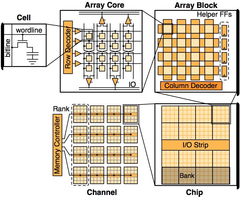
23 Current Structure 23

")

24 Photonics to the Chip Electrical Baseline (E1) Photonics Off-Chip w/electrical On-Chip (P1) 24
 8 Data Access Points per Column (P8)")
25 Photonics Into the Chip 2 Data Access Points per Column (P2) 8 Data Access Points per Column (P8) 25


26 Reducing Activate Energy Want to activate less bits while achieving the same access width Increase number of I/Os per array core, which decreases page size Compensate the area hit by smaller photonic off-chip I/O Initial Design Double the I/Os (and bandwidth) 26
27 Methodology Photonic Model - aggressive and conservative projections Model - Heavily modified CACTI-D Custom C++ architectural simulator running random traffic to animate models Setup is configurable, in this presentation: 1 chip to obtain 1GB capacity with >500Gbps of bandwidth provided by 64 banks 27

28 Energy for On/Off-Chip Floorplan 28


29 Reducing Row Size 4 I/Os per Array Core 32 I/Os per Array Core 29
30 Latency Not a Big Win Latency marginally better Most of latency is within array core Since array core mostly unchanged, latency only slightly improved by reduced serialization latency 30


31 Area Neutral 4 I/Os per Array Core 32 I/Os per Array Core 31


32 Scaling Capacity Motivation: allow the system to increase capacity without increasing bandwidth Shared Photonic Bus Vantrease et al., ISCA 2008 Disadvantage: high path loss (grows exponentially) due to couplers and waveguide 32


33 Split Photonic Bus Advantage: much lower path loss Disadvantage: all paths lit 33
34 Guided Photonic Bus Advantage: only 1 low loss path lit 34
35 Scaling Results Aggressive Photonic Device Specs 35
36 With Photonics... 10x memory bandwidth for same power Higher memory capacity without sacrificing bandwidth Area neutral Easily adapted to other storage technologies 36
37 Conclusion Computer interconnects are very complex microcommunication systems Cross-layer design approach is needed to solve the on-chip and off-chip interconnect problem Most important metrics Bandwidth-density (Gb/s/um) Energy-efficiency (mw/gb/s) Monolithic CMOS-photonics can improve the throughput by 10-20x But, need to be careful Optimize network design (electrical switching, optical transport) Use aggregation to increase link utilizations Optimize physical mapping (layout) for low optical insertion loss 37
38 Backup Slides


39 Photonic Technology Monolithically integrated silicon photonics being researched by MIT Center for Integrated Photonic Systems (CIPS) Orcutt et al., CLEO 2008 Holzwarth et al., CLEO 2008
40 Photonic Link Each wavelength can transmit at 10Gbps Dense Wave Division Multiplexing (DWDM) 64 wavelengths per direction in same media Rough Comparison Electrical Photonic Off-Chip I/O Energy (pj/bit) Off-Chip BW Density (Tbps/mm 2 )
41 Resonant Rings light not resonant resonant light resonant light w/ drop path figures inspired by [Vantrease, ISCA 08]
42 Ring Modulators Modulator uses charge injection to change resonant wavelength When resonant light passes it mostly gets trapped in ring resonant racetrack modulator modulator off
43 Ring Modulators Modulator uses charge injection to change resonant wavelength When resonant light passes it mostly gets trapped in ring resonant racetrack modulator modulator on
44 Photonic Components
45 Why 5pJ/b for Electrical? Prior work has claimed lower than our forecasted 5pJ/b for off-chip electrical I/O Gbps (Palmer et al., ISSCC 2007) Gbps (O Mahony et al., ISSCC 2010) Some important differences to consider: We assume 20Gbps per pin Otherwise will definitely be pin limited At higher data rates it is hard to be as energy efficient: 16Gbps (Lee et al., JSSC 2009) process has slower transistors leading to less energy efficient drivers Background energy averaged in (clocking, fixed energy, not 100% utilization)


46 Control Distribution Electrical Baseline & Control H-Tree Access Point Control distributed from the center of the chip H-tree spreads out to banks Photonic Floorplan showing Control Can power gate control lines to inactive banks


47 Full Energy Conservative Aggressive 64 Wavelengths, 4 I/Os 64 Wavelengths, 32 I/Os 8 Wavelengths, 32 I/Os


48 Conservative Utilization Aggressive 64 Wavelengths, 4 I/Os 64 Wavelengths, 32 I/Os 8 Wavelengths, 32 I/Os


49 Full Area 64 Wavelengths, 4 I/Os 64 Wavelengths, 32 I/Os 8 Wavelengths, 32 I/Os

50 Full Scaling Aggressive Conservative
Silicon-Photonic Clos Networks for Global On-Chip Communication
 Silicon-Photonic Clos Networks for Global On-Chip Communication Ajay Joshi, Christopher Batten, Yong-Jin Kwon, Scott Beamer, Imran Shamim, Krste Asanović, Vladimir Stojanović NOCS 2009 Massachusetts Institute
Building Manycore Processor-to-DRAM Networks with Monolithic Silicon Photonics
 Building Manycore Processor-to-DRAM Networks with Monolithic Silicon Photonics Christopher Batten 1, Ajay Joshi 1, Jason Orcutt 1, Anatoly Khilo 1 Benjamin Moss 1, Charles Holzwarth 1, Miloš Popović 1,
Addressing Link-Level Design Tradeoffs for Integrated Photonic Interconnects
 Addressing Link-Level Design Tradeoffs for Integrated Photonic Interconnects Michael Georgas, Jonathan Leu, Benjamin Moss, Chen Sun and Vladimir Stojanović Massachusetts Institute of Technology CICC 2011
Designing VLSI Interconnects with Monolithically Integrated Silicon-Photonics. Vladimir Stojanović MIT
 Designing VLSI Interconnects with Monolithically Integrated Silicon-Photonics Vladimir Stojanović MIT SSCS DL series Santa Clara, CA, November, 2012 Acknowledgments Rajeev Ram, Henry Smith, Hanqing Li
More-than-Moore with Integrated Silicon-Photonics. Vladimir Stojanović Berkeley Wireless Rearch Center UC Berkeley
 More-than-Moore with Integrated Silicon-Photonics Vladimir Stojanović Berkeley Wireless Rearch Center UC Berkeley 1 Acknowledgments Milos Popović (Boulder/BU), Rajeev Ram, Jason Orcutt, Hanqing Li (MIT),
Designing Future VLSI Systems with Monolithically Integrated Silicon-Photonics
 Designing Future VLSI Systems with Monolithically Integrated Silicon-Photonics Vladimir Stojanović University of California, Berkeley SSCS DL Lecture University of Texas, Austin November, 2013 2 Acknowledgments
Building Manycore Processor-to-DRAM Networks with Monolithic Silicon Photonics
 Appears in the Proceedings of the 16th Symposium on High Performance Interconnects (HOTI-16), August 2008 Building Manycore Processor-to-DRAM Networks with Monolithic Silicon Photonics Christopher Batten
PROBE: Prediction-based Optical Bandwidth Scaling for Energy-efficient NoCs
 PROBE: Prediction-based Optical Bandwidth Scaling for Energy-efficient NoCs Li Zhou and Avinash Kodi Technologies for Emerging Computer Architecture Laboratory (TEAL) School of Electrical Engineering and
TDM Photonic Network using Deposited Materials
 TDM Photonic Network using Deposited Materials ROBERT HENDRY, GILBERT HENDRY, KEREN BERGMAN LIGHTWAVE RESEARCH LAB COLUMBIA UNIVERSITY HPEC 2011 Motivation for Silicon Photonics Performance scaling becoming
The Light at the End of the Wire. Dana Vantrease + HP Labs + Mikko Lipasti
 The Light at the End of the Wire Dana Vantrease + HP Labs + Mikko Lipasti 1 Goals of This Talk Why should we (architects) be interested in optics? How does on-chip optics work? What can we build with optics?
Dynamic Reconfiguration of 3D Photonic Networks-on-Chip for Maximizing Performance and Improving Fault Tolerance
 Dynamic Reconfiguration of 3D Photonic Networks-on-Chip for Maximizing Performance and Improving Fault Tolerance Randy Morris Ϯ, Avinash Kodi Ϯ and Ahmed Louri School of Electrical Engineering and Computer
MODELING AND EVALUATION OF CHIP-TO-CHIP SCALE SILICON PHOTONIC NETWORKS
 1 MODELING AND EVALUATION OF CHIP-TO-CHIP SCALE SILICON PHOTONIC NETWORKS Robert Hendry, Dessislava Nikolova, Sébastien Rumley, Keren Bergman Columbia University HOTI 2014 2 Chip-to-chip optical networks
A 3.9 ns 8.9 mw 4 4 Silicon Photonic Switch Hybrid-Integrated with CMOS Driver
 A 3.9 ns 8.9 mw 4 4 Silicon Photonic Switch Hybrid-Integrated with CMOS Driver A. Rylyakov, C. Schow, B. Lee, W. Green, J. Van Campenhout, M. Yang, F. Doany, S. Assefa, C. Jahnes, J. Kash, Y. Vlasov IBM
Optical Bus for Intra and Inter-chip Optical Interconnects
 Optical Bus for Intra and Inter-chip Optical Interconnects Xiaolong Wang Omega Optics Inc., Austin, TX Ray T. Chen University of Texas at Austin, Austin, TX Outline Perspective of Optical Backplane Bus
Lecture: Integration of silicon photonics with electronics. Prepared by Jean-Marc FEDELI CEA-LETI
 Lecture: Integration of silicon photonics with electronics Prepared by Jean-Marc FEDELI CEA-LETI Context The goal is to give optical functionalities to electronics integrated circuit (EIC) The objectives
NEXT GENERATION SILICON PHOTONICS FOR COMPUTING AND COMMUNICATION PHILIPPE ABSIL
 NEXT GENERATION SILICON PHOTONICS FOR COMPUTING AND COMMUNICATION PHILIPPE ABSIL OUTLINE Introduction Platform Overview Device Library Overview What s Next? Conclusion OUTLINE Introduction Platform Overview
EE 232 Lightwave Devices Optical Interconnects
 EE 232 Lightwave Devices Optical Interconnects Sajjad Moazeni Department of Electrical Engineering & Computer Sciences University of California, Berkeley 1 Emergence of Optical Links US IT Map Hyper-Scale
A tunable Si CMOS photonic multiplexer/de-multiplexer
 A tunable Si CMOS photonic multiplexer/de-multiplexer OPTICS EXPRESS Published : 25 Feb 2010 MinJae Jung M.I.C.S Content 1. Introduction 2. CMOS photonic 1x4 Si ring multiplexer Principle of add/drop filter
A Nanophotonic Interconnect for High- Performance Many-Core Computation
 A Nanophotonic Interconnect for High- Performance Many-Core Computation Ray Beausoleil Quantum Optics Research Group Information and Quantum Systems HP Laboratories 008 Hewlett-Packard Development Company,
Silicon Optical Modulator
 Silicon Optical Modulator Silicon Optical Photonics Nature Photonics Published online: 30 July 2010 Byung-Min Yu 24 April 2014 High-Speed Circuits & Systems Lab. Dept. of Electrical and Electronic Engineering
IBM T. J. Watson Research Center IBM Corporation
 Broadband Silicon Photonic Switch Integrated with CMOS Drive Electronics B. G. Lee, J. Van Campenhout, A. V. Rylyakov, C. L. Schow, W. M. J. Green, S. Assefa, M. Yang, F. E. Doany, C. V. Jahnes, R. A.
Opportunities and challenges of silicon photonics based System-In-Package
 Opportunities and challenges of silicon photonics based System-In-Package ECTC 2014 Panel session : Emerging Technologies and Market Trends of Silicon Photonics Speaker : Stéphane Bernabé (Leti Photonics
Si photonics for the Zettabyte Era. Marco Romagnoli. CNIT & TeCIP - Scuola Superiore Sant Anna
 Si photonics for the Zettabyte Era Marco Romagnoli CNIT & TeCIP - Scuola Superiore Sant Anna Semicon 2013 Dresden 8-10 October 2013 Zetabyte era Disaggregation at system level Integration at chip level
Device Requirements for Optical Interconnects to Silicon Chips
 To be published in Proc. IEEE Special Issue on Silicon Photonics, 2009 Device Requirements for Optical Interconnects to Silicon Chips David A. B. Miller, Fellow, IEEE Abstract We examine the current performance
Performance and Energy Trade-offs for 3D IC NoC Interconnects and Architectures
 Rochester Institute of Technology RIT Scholar Works Theses Thesis/Dissertation Collections 1-215 Performance and Energy Trade-offs for 3D IC NoC Interconnects and Architectures James David Coddington Follow
Transmission-Line-Based, Shared-Media On-Chip. Interconnects for Multi-Core Processors
 Design for MOSIS Educational Program (Research) Transmission-Line-Based, Shared-Media On-Chip Interconnects for Multi-Core Processors Prepared by: Professor Hui Wu, Jianyun Hu, Berkehan Ciftcioglu, Jie
A high-speed, tunable silicon photonic ring modulator integrated with ultra-efficient active wavelength control
 A high-speed, tunable silicon photonic ring modulator integrated with ultra-efficient active wavelength control Xuezhe Zheng, 1 Eric Chang, 2 Philip Amberg, 1 Ivan Shubin, 1 Jon Lexau, 2 Frankie Liu, 2
Parallel Computing 2020: Preparing for the Post-Moore Era. Marc Snir
 Parallel Computing 2020: Preparing for the Post-Moore Era Marc Snir THE (CMOS) WORLD IS ENDING NEXT DECADE So says the International Technology Roadmap for Semiconductors (ITRS) 2 End of CMOS? IN THE LONG
Thermal Management of Manycore Systems with Silicon-Photonic Networks
 Thermal Management of Manycore Systems with Silicon-Photonic Networks Tiansheng Zhang, José L. Abellán, Ajay Joshi, Ayse K. Coskun Electrical and Computer Engineering Department, Boston University, Boston,
Challenges for On-chip Optical Interconnect
 Initial Results of Prototyping a 3-D Integrated Intra-Chip Free-Space Optical Interconnect Berkehan Ciftcioglu, Rebecca Berman, Jian Zhang, Zach Darling, Alok Garg, Jianyun Hu, Manish Jain, Peng Liu, Ioannis
ISSCC 2006 / SESSION 13 / OPTICAL COMMUNICATION / 13.7
 13.7 A 10Gb/s Photonic Modulator and WDM MUX/DEMUX Integrated with Electronics in 0.13µm SOI CMOS Andrew Huang, Cary Gunn, Guo-Liang Li, Yi Liang, Sina Mirsaidi, Adithyaram Narasimha, Thierry Pinguet Luxtera,
OPTICAL I/O RESEARCH PROGRAM AT IMEC
 OPTICAL I/O RESEARCH PROGRAM AT IMEC IMEC CORE CMOS PHILIPPE ABSIL, PROGRAM DIRECTOR JORIS VAN CAMPENHOUT, PROGRAM MANAGER SCALING TRENDS IN CHIP-LEVEL I/O RECENT EXAMPLES OF HIGH-BANDWIDTH I/O Graphics
ON THE WAY TO PHOTONIC INTERPOSERS, BUILDING BLOCKS FOR USR-OPTICAL COMMUNICATION. OPTICS Workshop DATE 2017 Yvain THONNART Mar.
 ON THE WAY TO PHOTONIC INTERPOSERS, BUILDING BLOCKS FOR USR-OPTICAL COMMUNICATION OUTLINE Motivations Interposer technologies for manycores Our goal An optically interconnected manycore on interposer Silicon
A 32 Gbps 2048-bit 10GBASE-T Ethernet Energy Efficient LDPC Decoder with Split-Row Threshold Decoding Method
 A 32 Gbps 248-bit GBASE-T Ethernet Energy Efficient LDPC Decoder with Split-Row Threshold Decoding Method Tinoosh Mohsenin and Bevan M. Baas VLSI Computation Lab, ECE Department University of California,
ECEN689: Special Topics in High-Speed Links Circuits and Systems Spring 2012
 ECEN689: Special Topics in High-Speed Links Circuits and Systems Spring 2012 Lecture 5: Termination, TX Driver, & Multiplexer Circuits Sam Palermo Analog & Mixed-Signal Center Texas A&M University Announcements
Si Photonics Technology Platform for High Speed Optical Interconnect. Peter De Dobbelaere 9/17/2012
 Si Photonics Technology Platform for High Speed Optical Interconnect Peter De Dobbelaere 9/17/2012 ECOC 2012 - Luxtera Proprietary www.luxtera.com Overview Luxtera: Introduction Silicon Photonics: Introduction
Comparison of Bandwidth Limits for On-card Electrical and Optical Interconnects for 100 Gb/s and Beyond
 Invited Paper Comparison of Bandwidth Limits for On-card Electrical and Optical Interconnects for 1 Gb/s and Beyond Petar Pepeljugoski *, Mark Ritter, Jeffrey A. Kash, Fuad Doany, Clint Schow, Young Kwark,
Silicon photonics integration roadmap for applications in computing systems
 Silicon photonics integration roadmap for applications in computing systems Bert Jan Offrein Neuromorphic Devices and Systems Group 2016 IBM Corporation Outline Photonics and computing? The interconnect
Design Space Exploration of Optical Interfaces for Silicon Photonic Interconnects
 Design Space Exploration of Optical Interfaces for Silicon Photonic Interconnects Olivier Sentieys, Johanna Sepúlveda, Sébastien Le Beux, Jiating Luo, Cedric Killian, Daniel Chillet, Ian O Connor, Hui
Electronic-Photonic ICs for Low Cost and Scalable Datacenter Solutions
 Electronic-Photonic ICs for Low Cost and Scalable Datacenter Solutions Christoph Theiss, Director Packaging Christoph.Theiss@sicoya.com 1 SEMICON Europe 2016, October 27 2016 Sicoya Overview Spin-off from
Interconnect-Power Dissipation in a Microprocessor
 4/2/2004 Interconnect-Power Dissipation in a Microprocessor N. Magen, A. Kolodny, U. Weiser, N. Shamir Intel corporation Technion - Israel Institute of Technology 4/2/2004 2 Interconnect-Power Definition
Index. Cambridge University Press Silicon Photonics Design Lukas Chrostowski and Michael Hochberg. Index.
 absorption, 69 active tuning, 234 alignment, 394 396 apodization, 164 applications, 7 automated optical probe station, 389 397 avalanche detector, 268 back reflection, 164 band structures, 30 bandwidth
ECEN620: Network Theory Broadband Circuit Design Fall 2014
 ECEN620: Network Theory Broadband Circuit Design Fall 2014 Lecture 19: High-Speed Transmitters Sam Palermo Analog & Mixed-Signal Center Texas A&M University Announcements Exam 3 is on Friday Dec 5 Focus
Convergence Challenges of Photonics with Electronics
 Convergence Challenges of Photonics with Electronics Edward Palen, Ph.D., P.E. PalenSolutions - Optoelectronic Packaging Consulting www.palensolutions.com palensolutions@earthlink.net 415-850-8166 October
ECEN689: Special Topics in Optical Interconnects Circuits and Systems Spring 2016
 ECEN689: Special Topics in Optical Interconnects Circuits and Systems Spring 2016 Lecture 1: Introduction Sam Palermo Analog & Mixed-Signal Center Texas A&M University Class Topics System and design issues
On-Chip Optical Interconnects: Prospects and Challenges
 6th International Conference of Soft Computing and Pattern Recognition, August 11-14, 2014, Tunis, Tunisia On-Chip Optical Interconnects: Prospects and Challenges Abderazek Ben Abdallah The University
Si CMOS Technical Working Group
 Si CMOS Technical Working Group CTR, Spring 2008 meeting Markets Interconnects TWG Breakouts Reception TWG reports Si CMOS: photonic integration E-P synergy - Integration - Standardization - Cross-market
IEEE JOURNAL OF SELECTED TOPICS IN QUANTUM ELECTRONICS 2010 Silicon Photonic Circuits: On-CMOS Integration, Fiber Optical Coupling, and Packaging
 IEEE JOURNAL OF SELECTED TOPICS IN QUANTUM ELECTRONICS 2010 Silicon Photonic Circuits: On-CMOS Integration, Fiber Optical Coupling, and Packaging Christophe Kopp, St ephane Bernab e, Badhise Ben Bakir,
Lecture 04 CSE 40547/60547 Computing at the Nanoscale Interconnect
 Lecture 04 CSE 40547/60547 Computing at the Nanoscale Interconnect Introduction - So far, have considered transistor-based logic in the face of technology scaling - Interconnect effects are also of concern
Practical Limitations of State of the Art Passive Printed Circuit Board Power Delivery Networks for High Performance Compute Systems
 Practical Limitations of State of the Art Passive Printed Circuit Board Power Delivery Networks for High Performance Compute Systems Presented by Chad Smutzer Mayo Clinic Special Purpose Processor Development
Multiband RF-Interconnect for Reconfigurable Network-on-Chip Communications UCLA
 Multiband RF-Interconnect for Reconfigurable Network-on-hip ommunications Jason ong (cong@cs.ucla.edu) Joint work with Frank hang, Glenn Reinman and Sai-Wang Tam ULA 1 ommunication hallenges On-hip Issues
- no emitters/amplifiers available. - complex process - no CMOS-compatible
 Advantages of photonic integrated circuits (PICs) in Microwave Photonics (MWP): compactness low-power consumption, stability flexibility possibility of aggregating optics and electronics functionalities
Jason Cong, Glenn Reinman.
 RF Interconnects for Communications On-chip 1 M.-C. Frank Chang, Eran Socher, Sai-Wang Tam Electrical Engineering Dept. UCLA Los Angeles, CA 90095 001-1-310-794-1633 {mfchang,socher,roccotam}@ee.ucla.edu
ECEN689: Special Topics in Optical Interconnects Circuits and Systems Spring 2016
 ECEN689: Special Topics in Optical Interconnects Circuits and Systems Spring 2016 Lecture 10: Electroabsorption Modulator Transmitters Sam Palermo Analog & Mixed-Signal Center Texas A&M University Announcements
Innovations in Photonic Integration Platforms
 Innovations in Photonic Integration Platforms September 20, 20 Burgeoning Growth Demand Disruptive Technology Video content is fast becoming a larger percentage of total internet traffic 50% Video services
Silicon Photonics Transceivers for Hyper Scale Datacenters: Deployment and Roadmap
 Silicon Photonics Transceivers for Hyper Scale Datacenters: Deployment and Roadmap Peter De Dobbelaere Luxtera Inc. 09/19/2016 Luxtera Proprietary www.luxtera.com Luxtera Company Introduction $100B+ Shift
ESE532: System-on-a-Chip Architecture. Today. Message. Crossbar. Interconnect Concerns
 ESE532: System-on-a-Chip Architecture Day 19: March 29, 2017 Network-on-a-Chip (NoC) Today Ring 2D Mesh Networks Design Issues Buffering and deflection Dynamic and static routing Penn ESE532 Spring 2017
Communications. Mitchell Fields, Ph. D. Director of Strategic Marketing
 Optical Navigation Division Optical Interconnects for Chip-to-Chip Communications Mitchell Fields, Ph. D. Director of Strategic Marketing mitch.h.fields@avagotech.comh com Contributors: Avago: Christine
D6.3: Evaluation of the 2nd generation 2x2 PLATON optical interconnect router
 ICT - Information and Communication Technologies Merging Plasmonics and Silicon Photonics Technology towards Tb/s routing in optical interconnects Collaborative Project Grant Agreement Number 249135 D6.3:
Cisco PONC Pavan Voruganti Senior Product Manager. March 2015
 Cisco PONC 2015 Pavan Voruganti Senior Product Manager March 2015 Bandwidth Explosion With a progressive uptake of video, IP, audio and cloud the compound annual growth rate (CAGR) of IP traffic is above
DSENT A Tool Connecting Emerging Photonics with Electronics for Opto-Electronic Networks-on-Chip Modeling
 Sixth IEEE/ACM International Symposium on Networks-on-Chip DSENT A Tool Connecting Emerging Photonics with Electronics for Opto-Electronic Networks-on-Chip Modeling Chen Sun, Chia-Hsin Owen Chen, George
Addressing Link-Level Design Tradeoffs for Integrated Photonic Interconnects
 Addressing Link-Level Design Tradeoffs for Integrated Photonic Interconnects Michael Georgas, Jonathan Leu, Benjamin Moss, Chen Sun, and Vladimir Stojanović Department of Electrical Engineering and Computer
Silicon Photonics Technology Platform To Advance The Development Of Optical Interconnects
 Silicon Photonics Technology Platform To Advance The Development Of Optical Interconnects By Mieke Van Bavel, science editor, imec, Belgium; Joris Van Campenhout, imec, Belgium; Wim Bogaerts, imec s associated
UNIVERSITY OF MASSACHUSETTS Dept. of Electrical & Computer Engineering. Computer Architecture ECE 568
 UNIVERSITY OF MASSACHUSETTS Dept. of Electrical & Computer Engineering Computer Architecture ECE 568 Part 14 Improving Performance: Interleaving Israel Koren ECE568/Koren Part.14.1 Background Performance
Optical Networks emerging technologies and architectures
 Optical Networks emerging technologies and architectures Faculty of Computer Science, Electronics and Telecommunications Department of Telecommunications Artur Lasoń 100 Gb/s PM-QPSK (DP-QPSK) module Hot
Chapter 7 Introduction to 3D Integration Technology using TSV
 Chapter 7 Introduction to 3D Integration Technology using TSV Jin-Fu Li Department of Electrical Engineering National Central University Jungli, Taiwan Outline Why 3D Integration An Exemplary TSV Process
Silicon Photonics for Mid-Board Optical Modules Marc Epitaux
 Silicon Photonics for Mid-Board Optical Modules Marc Epitaux Chief Architect at Samtec, Inc Outline Interconnect Solutions Mid-Board Optical Modules Silicon Photonics o Benefits o Challenges DragonFly
PhoenixSim: A Simulator for Physical-Layer Analysis of Chip-Scale Photonic Interconnection Networks
 PhoenixSim: A Simulator for Physical-Layer Analysis of Chip-Scale Photonic Interconnection Networks Johnnie Chan, Gilbert Hendry, Aleksandr Biberman, Keren Bergman Department of Electrical Engineering
Silicon Photonics in Optical Communications. Lars Zimmermann, IHP, Frankfurt (Oder), Germany
, Germany") Silicon Photonics in Optical Communications Lars Zimmermann, IHP, Frankfurt (Oder), Germany Outline IHP who we are Silicon photonics Photonic-electronic integration IHP photonic technology Conclusions
Silicon Photonics in Optical Communications Lars Zimmermann, IHP, Frankfurt (Oder), Germany Outline IHP who we are Silicon photonics Photonic-electronic integration IHP photonic technology Conclusions
Photo-Electronic Crossbar Switching Network for Multiprocessor Systems
 Photo-Electronic Crossbar Switching Network for Multiprocessor Systems Atsushi Iwata, 1 Takeshi Doi, 1 Makoto Nagata, 1 Shin Yokoyama 2 and Masataka Hirose 1,2 1 Department of Physical Electronics Engineering
RF Interconnects for Communications On-chip*
 RF Interconnects for Communications On-chip* M.-C. Frank Chang, Eran Socher, Sai-Wang Tam Electrical Engineering Dept. UCLA Los Angeles, CA 90095 001-1-310-794-1633 {mfchang,socher,roccotam}@ee.ucla.edu
EECS 427 Lecture 22: Low and Multiple-Vdd Design
 EECS 427 Lecture 22: Low and Multiple-Vdd Design Reading: 11.7.1 EECS 427 W07 Lecture 22 1 Last Time Low power ALUs Glitch power Clock gating Bus recoding The low power design space Dynamic vs static EECS
BANDWIDTH LIMITATIONS IN FUTURE MANY-CORE PROCESSORS. THIS ARTICLE FIRST
 ... UILING ANY-ORE PROESSOR-TO-RA NETWORKS WITH ONOLITHI OS SILION PHOTONIS... hristopher atten Ajay Joshi Jason Orcutt Anatol Khilo enjamin oss harles W. Holzwarth iloš A. Popović Hanqing Li Henry I.
Integrated Photonics using the POET Optical InterposerTM Platform
 Integrated Photonics using the POET Optical InterposerTM Platform Dr. Suresh Venkatesan CIOE Conference Shenzhen, China Sept. 5, 2018 POET Technologies Inc. TSXV: PUBLIC POET PTK.V Technologies Inc. PUBLIC
Mitigation of Mode Partition Noise in Quantum-dash Fabry-Perot Mode-locked Lasers using Manchester Encoding
 Mitigation of Mode Partition Noise in Quantum-dash Fabry-Perot Mode-locked Lasers using Manchester Encoding Mohamed Chaibi*, Laurent Bramerie, Sébastien Lobo, Christophe Peucheret *chaibi@enssat.fr FOTON
Technology Timeline. Transistors ICs (General) SRAMs & DRAMs Microprocessors SPLDs CPLDs ASICs. FPGAs. The Design Warrior s Guide to.
 SRAMs & DRAMs Microprocessors SPLDs CPLDs ASICs. FPGAs. The Design Warrior s Guide to.") FPGAs 1 CMPE 415 Technology Timeline 1945 1950 1955 1960 1965 1970 1975 1980 1985 1990 1995 2000 Transistors ICs (General) SRAMs & DRAMs Microprocessors SPLDs CPLDs ASICs FPGAs The Design Warrior s Guide
FPGAs 1 CMPE 415 Technology Timeline 1945 1950 1955 1960 1965 1970 1975 1980 1985 1990 1995 2000 Transistors ICs (General) SRAMs & DRAMs Microprocessors SPLDs CPLDs ASICs FPGAs The Design Warrior s Guide
Petar Pepeljugoski IBM T.J. Watson Research Center
 Comparison of Bandwidth Limits for On-Card Electrical and Optical Interconnects for 100 Gb/s and Beyond Petar Pepeljugoski IBM T.J. Watson Research Center Collaborators and Acknowledgements Fuad Doany,
LSI and Circuit Technologies for the SX-8 Supercomputer
 LSI and Circuit Technologies for the SX-8 Supercomputer By Jun INASAKA,* Toshio TANAHASHI,* Hideaki KOBAYASHI,* Toshihiro KATOH,* Mikihiro KAJITA* and Naoya NAKAYAMA This paper describes the LSI and circuit
Photonics Integration and Evolution of the Optical Transceiver Presented by: Giacomo Losio ProLabs
 Photonics Integration and Evolution of the Optical Transceiver Presented by: Giacomo Losio ProLabs Optical Transceivers architecture is challenged Electrical Driver TIA Laser Photodiode Optical Optical
Measurement Results for a High Throughput MCM
 Measurement Results for a High Throughput MCM Funding: Paul Franzon Toby Schaffer, Alan Glaser, Steve Lipa North Carolina State University paulf@ncsu.edu www.ece.ncsu.edu/erl Outline > Heterogeneous System
Silicon Photonics Photo-Detector Announcement. Mario Paniccia Intel Fellow Director, Photonics Technology Lab
 Silicon Photonics Photo-Detector Announcement Mario Paniccia Intel Fellow Director, Photonics Technology Lab Agenda Intel s Silicon Photonics Research 40G Modulator Recap 40G Photodetector Announcement
Low Transistor Variability The Key to Energy Efficient ICs
 Low Transistor Variability The Key to Energy Efficient ICs 2 nd Berkeley Symposium on Energy Efficient Electronic Systems 11/3/11 Robert Rogenmoser, PhD 1 BEES_roro_G_111103 Copyright 2011 SuVolta, Inc.
Impact of High-Speed Modulation on the Scalability of Silicon Photonic Interconnects
 Impact of High-Speed Modulation on the Scalability of Silicon Photonic Interconnects OPTICS 201, March 18 th, Dresden, Germany Meisam Bahadori, Sébastien Rumley,and Keren Bergman Lightwave Research Lab,
Integrated electro-optical waveguide based devices with liquid crystals on a silicon backplane
 Integrated electro-optical waveguide based devices with liquid crystals on a silicon backplane Florenta Costache Group manager Smart Micro-Optics SMO/AMS Fraunhofer Institute for Photonic Microsystems,
UNIT-II LOW POWER VLSI DESIGN APPROACHES
 UNIT-II LOW POWER VLSI DESIGN APPROACHES Low power Design through Voltage Scaling: The switching power dissipation in CMOS digital integrated circuits is a strong function of the power supply voltage.
New silicon photonics technology delivers faster data traffic in data centers
 Edition May 2017 Silicon Photonics, Photonics New silicon photonics technology delivers faster data traffic in data centers New transceiver with 10x higher bandwidth than current transceivers. Today, the
Cisco s CLEC Networkers Power Session
 Course Number Presentation_ID 1 Cisco s CLEC Networkers Power Session Session 2 The Business Case for ONS 15800 3 What s Driving the Demand? Data Voice 4 What s Driving the Demand? Internet 36,700,000
Monolithic Integra/on of O-band Photonic Transceivers in a Zero-change 32nm SOI CMOS
 Monolithic Integra/on of O-band Photonic Transceivers in a Zero-change 32nm SOI CMOS S. Moazeni 1, A. Atabaki 2, D. Cheian 2, S. Lin 1, R. J. Ram 2, and V. Stojanović 1 1 Department of EECS, University
Photonic Integrated Beamformer for Broadband Radio Astronomy
 M. Burla, D. A. I. Marpaung, M. R. H. Khan, C. G. H. Roeloffzen Telecommunication Engineering group University of Twente, Enschede, The Netherlands P. Maat, K. Dijkstra ASTRON, Dwingeloo, The Netherlands
Communication is ubiquitous; communication is the central fabric of human existence.
 DARPATech, DARPA s 25 th Systems and Technology Symposium August 7, 2007 Anaheim, California Teleprompter Script for Dr. Jagdeep Shah, Program Manager, Microsystems Technology Office COMMUNICATIONS: THE
Emerging Highly Compact Amplification Solutions for Coherent Transmission
 Emerging Highly Compact Amplification Solutions for Coherent Transmission Market Focus ECOC 2017 Sep 20, 2017 Dr. Sanjai Parthasarathi Vice President, Product Marketing & Strategy II-VI Photonics Outline
Physical Layer Analysis and Modeling of Silicon Photonic WDM Bus Architectures
 Physical Layer Analysis and Modeling of Silicon Photonic WDM Bus Architectures Robert Hendry, Dessislava Nikolova, Sebastien Rumley, Noam Ophir, Keren Bergman Columbia University 6 th St. and Broadway
Zukunftstechnologie Dünnglasbasierte elektrooptische. Research Center of Microperipheric Technologies
 Zukunftstechnologie Dünnglasbasierte elektrooptische Baugruppenträger Dr. Henning Schröder Fraunhofer IZM, Berlin, Germany Today/Overview Motivation: external roadmaps High Bandwidth and Channel Density
20Gb/s 0.13um CMOS Serial Link
 20Gb/s 0.13um CMOS Serial Link Patrick Chiang (pchiang@stanford.edu) Bill Dally (billd@csl.stanford.edu) Ming-Ju Edward Lee (ed@velio.com) Computer Systems Laboratory Stanford University Stanford University
MTO Technology Programs Progress. Frank Stroili Technical Director, RF/Mixed signal
 MTO Technology Programs Progress Frank Stroili Technical Director, RF/Mixed signal 603-885-7487 frank.stroili@baesystems.com 1 Report Documentation Page Form Approved OMB No. 0704-0188 Public reporting
Low-Power VLSI. Seong-Ook Jung VLSI SYSTEM LAB, YONSEI University School of Electrical & Electronic Engineering
 Low-Power VLSI Seong-Ook Jung 2013. 5. 27. sjung@yonsei.ac.kr VLSI SYSTEM LAB, YONSEI University School of Electrical & Electronic Engineering Contents 1. Introduction 2. Power classification & Power performance
Synthesis of Optimal On-Chip Baluns
 Synthesis of Optimal On-Chip Baluns Sharad Kapur, David E. Long and Robert C. Frye Integrand Software, Inc. Berkeley Heights, New Jersey Yu-Chia Chen, Ming-Hsiang Cho, Huai-Wen Chang, Jun-Hong Ou and Bigchoug
Practical Information
 EE241 - Spring 2010 Advanced Digital Integrated Circuits TuTh 3:30-5pm 293 Cory Practical Information Instructor: Borivoje Nikolić 550B Cory Hall, 3-9297, bora@eecs Office hours: M 10:30am-12pm Reader:
DATE 2016 Early Reliability Modeling for Aging and Variability in Silicon System (ERMAVSS Workshop)
") March 2016 DATE 2016 Early Reliability Modeling for Aging and Variability in Silicon System (ERMAVSS Workshop) Ron Newhart Distinguished Engineer IBM Corporation March 19, 2016 1 2016 IBM Corporation Background
March 2016 DATE 2016 Early Reliability Modeling for Aging and Variability in Silicon System (ERMAVSS Workshop) Ron Newhart Distinguished Engineer IBM Corporation March 19, 2016 1 2016 IBM Corporation Background
AS core count increases in manycore systems to support
 IEEE TRANSACTIONS ON COMPUTER-AIDED DESIGN OF INTEGRATED CIRCUITS AND SYSTEMS, VOL. 36, NO. 5, MAY 2017 801 Adaptive Tuning of Photonic Devices in a Photonic NoC Through Dynamic Workload Allocation José