More-than-Moore with Integrated Silicon-Photonics. Vladimir Stojanović Berkeley Wireless Rearch Center UC Berkeley
|
|
|
- Antony Neal Cole
- 5 years ago
- Views:
Transcription
1 More-than-Moore with Integrated Silicon-Photonics Vladimir Stojanović Berkeley Wireless Rearch Center UC Berkeley 1
2 Acknowledgments Milos Popović (Boulder/BU), Rajeev Ram, Jason Orcutt, Hanqing Li (MIT), Krste Asanović (UC Berkeley) Jeffrey Shainline, Christopher Batten, Ajay Joshi, Anatoly Khilo Mark Wade, Karan Mehta, Jie Sun, Josh Wang Chen Sun, Sen Lin, Sajjad Moazeni, Nandish Mehta, Michael Georgas, Benjamin Moss, Jonathan Leu Yong-Jin Kwon, Scott Beamer, Yunsup Lee, Andrew Waterman, Miquel Planas, Rimas Avizienis, Henry Cook, Huy Vo Roy Meade, Gurtej Sandhu and Micron Fab12 team (Zvi, Ofer, Daniel, Efi, Elad, ) DARPA, Micron, NSF, BWRC IBM Trusted Foundry, Global Foundries Slide 2


3 3 More-than-Moore perspective Enhanced CMOS enables new applications 1997 One of the first CMOS radios Rudell & Gray 2004 World s first 60GHz CMOS Amplifier Niknejad & Brodersen 2012 World s first siphotonic transmitter in 45nm SOI Stojanovic, Popovic, Ram Inductors in IC process Nguyen & Meyer 1990
 CMOS")


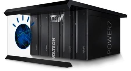
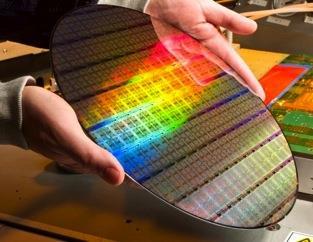
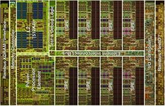
4 IBM/GF 12SOI (45nm) CMOS 300mm wafer, commercial process MOSIS and TAPO MPW access Advanced process used in microprocessors Photonic enhancement enables VLSI photonic systems (no required process changes) IBM Cell IBM Espresso IBM Power 7
![Zero-Change Photonics in 45nm [C. Sun, JSSC 2016] Photonics for free!](/docs-images/80/82520119/images/5-1.jpg "(No modification to the process) Closest proximity of electronics and photonics Single substrate removal post-processing")
5 Zero-Change Photonics in 45nm [C. Sun, JSSC 2016] Photonics for free! (No modification to the process) Closest proximity of electronics and photonics Single substrate removal post-processing step Monolithic photonics platform with fastest transistors

6 Integrated photonic interconnects Each λ carries one bit of data Bandwidth Density achieved through DWDM Energy-efficiency achieved through low-loss optical components and tight integration Slide 6


7 Single channel link tradeoffs Loss 10-dB 15-dB Rx Cap 5-fF 25-fF 7


8 Need to optimize carefully 512 Gb/s aggregate throughput Laser energy increases with data-rate Limited Rx sensitivity Modulation more expensive -> lower extinction ratio Tuning costs decrease with data-rate Moderate data rates most energy-efficient assuming 32nm CMOS Georgas CICC
9 DWDM link efficiency optimization Optimize for min energy-cost Bandwidth density dominated by circuit and photonics area (not coupler pitch) Slide 9
 Micron D1L")

10 6mm 5mm Towards an Optical DRAM System EOS22 Test Chip High Performance 45nm SOI Photonic-Interconnected DRAM (PIM) Micron D1L Test Chip Power-optimized 0.22µm Bulk [ISCA 2010] 2M transistors 1000s optical devices 70M transistors 1000 optical devices DARPA POEM Slide 10

11 World s First Processor to Communicate with Light Silicon-Photonic components integrated directly in the chip zero-change 45nm SOI DARPA POEM & PERFECT Stojanović, Asanović C. Sun et al. Nature, Dec
12 Frequency (MHz) Processor Cores 45nm SOI Vdd (V) Gflops/W Not Operational RISC-V open ISA Scalar-vector cores - Boot Linux GHz, 4-16 GFlops/W Slide 12 [Lee ESSCIRC 2014]
13 Si Waveguides 470nm width 700nm width
![Key Device Components Vertical couplers Waveguide Diffraction Grating Waveguide Taper Slide 14 [Wade OIC 2015]](/docs-images/80/82520119/images/14-1.jpg "submitted to Nature August 2015 please keep confidential funded in part by DARPA POEM program, Stojanovic, Asanovic,")
14 Key Device Components Vertical couplers Waveguide Diffraction Grating Waveguide Taper Slide 14 [Wade OIC 2015] submitted to Nature August 2015 please keep confidential funded in part by DARPA POEM program, Stojanovic, Asanovic, Popovic, Ram


15 Key Device Components SiGe from PMOS strain engineering used in Photodetectors SiGe Photodetector Waveguide Taper Waveguide Slide 15 [Orcutt 2013, Alloatti APL 2015]

16 Key Device Components Modulator Microring Drop Waveguide Integrated Heater Output Waveguide Input Waveguide [Shainline OL 2013, Wade OFC 2014] Slide 16


17 Transmitter Modulator In/Out Grating Couplers V BIAS PRBS31 8:1 Modulator Driver Transmit Site 50um In Driven by a CMOS logic inverter (1.2V pp ) 5 Gb/s data rate at ~30fJ/b with >6dB extinction ratio, 3dB insertion loss Up to 12 Gb/s with 2-3dB extinction [Wade OFC 2014] [Sun VLSI 2015] Slide 17

18 Receiver Receive Site 50um 5k Ω Receiver BER Checker TIA - + φ Out A Input Grating Coupler 2:8 5k Ω Dummy TIA - + Clock Buffers φ Out B V PD Photodetector Low parasitics from monolithic integration enable single-stage 5kΩ TIA receiver 10 Gb/s operation at 290 fj/bit with 8.3uA sensitivity [Georgas VLSI 2014] Slide 18
19 5 Gb/s Chip-to-Chip Link Laser Power 1189nm Laser 3.8 dbm Decision Threshold [ua] Thermal Tuner PD -0.2 dbm Chip 1 Bit 1 Bit 0 Tx Rx Out A PRBS31 8:1-3.2 dbm dbm -7.2 dbm dbm Optical Amplifier 0.8 dbm -5.9 dbm Time [ps] Chip 2 PD Rx Out B BER Check 2:8 Rx -3.2 dbm 9.65uA -9.9 dbm 2.04uA 1e-001 1e-002 1e-003 1e-004 1e-005 1e-006 1e-007 1e-008 1e-009 1e-010 <1e-010 Bit 1 Bit 0 Slide 19
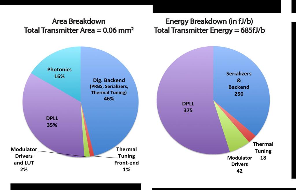
20 5 Gb/s Link Efficiency Summary Thermal Tuning* 275 fj/bit (42%) Modulator Driver 30 fj/bit (5%) Optical power: 3.6mW (13mW extrapolated without amplifier) 662 fj/bit for circuits Receiver 357 fj/bit (54%) zero-change monolithic competitive with state-of-the-art heterogeneous platforms 680 fj/bit, 14mW optical power [Zheng PTL 2012**] *Includes all closed-loop circuits nm tuning power **0.5nm tuning power only Slide 20
 662 fj/bit for circuits Receiver 357 fj/bit (54%) 560 fj/bit for laser wall-plug** Not using our best devices in the link 1dB loss couplers [Wade, OIC 2015]")
21 5 Gb/s Link Efficiency Summary Thermal Tuning* 275 fj/bit (42%) Modulator Driver 30 fj/bit (5%) Optical power: 3.6mW (13mW extrapolated without amplifier) 662 fj/bit for circuits Receiver 357 fj/bit (54%) 560 fj/bit for laser wall-plug** Not using our best devices in the link 1dB loss couplers [Wade, OIC 2015] (on the same chip instead of 4dB in the link) 5-10x better photodetector ( A/W photodetector on the same chip) Expect to obtain >40x smaller laser power (65fJ/b optical) **11.6% QD laser wall-plug efficiency *Includes all closed-loop circuits nm tuning power Slide 21


22 Electronic-Photonic Packaging Die-thinned chip with selective substrate removal WDM transceiver regions Epoxy Processor and SRAM regions Flip-chip onto FR4 PCB using C4 bumps Selective substrate removal of optical transceiver regions Slide 22
23 Memory Controller PD RISC-V Processor Interface PD 1MB Memory Array Optical Memory System Demo Chip (Processor Mode) Memory to processor link read data Chip (Memory Mode) 1MB Memory Array (Inactive) Receiver Optical Amplifier Transmitter Laser 50/50 Power Splitter Single-Mode Fiber Transmitter Optical Amplifier Receiver RISC-V Processor (Inactive) Command + address + write data Processor to memory link Chip 1 acts as processor, Chip 2 acts as memory Custom memory controller, DRAM interface emulator Takes advantage of full duplex (as opposed to half-duplex) memory interface Video demonstration (thermal stress test)
24 Transmission [db] Tx and Rx DWDM Transceiver Banks Transmission [db] Wavelength [nm] -2 Tx Rx Wavelength [nm] Advanced lithography enables tight ring resonance control

![auto-locked [Sun JSSC 2016] Slice 0 Slice 1 Slice 2 Slice 3 Slice 4 Slice 5 Slice 6 Slice](/docs-images/80/82520119/images/25-2.jpg "7 Slice 8 Slice 9 Slice 10 >8 Gb/s limited by duty-cycle distortion of off-chip clock")
25 11 x 8 Gbps Tx Demonstration 11 rings, each demonstrating 8 Gbps modulation Independently testing one at a time Potential for 88 Gb/s on a single fiber/waveguide Each ring is auto-locked [Sun JSSC 2016] Slice 0 Slice 1 Slice 2 Slice 3 Slice 4 Slice 5 Slice 6 Slice 7 Slice 8 Slice 9 Slice 10 >8 Gb/s limited by duty-cycle distortion of off-chip clock source

26 Going Faster PAM2 and PAM4 [Moazeni et al, ISSCC 2017] Direct Digital-to-Optical Conversion!

27 Chip floorplan
: 5.")
28 Transmitter eye diagrams Extinction ratio (ER): 3dB, Insertion loss (IL): 5.5dB PAM4 coding used: (0,5,10,15) 42fJ/b driver energy efficiency
29 Transmitter specs 29

30 Improved Rx Topologies Leverage tight electronic-photonic integration to create new, more sensitive receiver structures Differential, DDR receiver [Nandish Mehta et al. ESSCIRC16]
31 Platform Performance Summary Metric [Beamer ISCA 2010] Conservative Estimates 45nm SOI Platform Bulk Photonics Platform* Waveguide Loss 4 db/cm 3.7 db/cm 10.5 db/cm Vertical Coupler Loss 1 db 1 db 3 db Tx Data Rate 10 Gb/s 20 Gb/s 5 Gb/s Tx Energy Per Bit 120 fj/b 42 fj/b 350 fj/b Rx Data Rate 10 Gb/s 12 Gb/s 5 Gb/s Rx Energy Per Bit 80 fj/b 297 fj/b 1700 fj/b Rx Sensitivity 10 μa 8 μa 36 μa PD Responsivity 0.9 A/W 0.44 A/W 0.2 A/W Thermal Tuning Efficiency 1.6 μw/ghz 3.8 μw/ghz 10 μw/ghz Comparison to a proposal for the processor-memory system we published 6 years ago Meeting/exceeding most system specs Slide 31 *considerably slower process than one assumed in [Beamer ISCA 2010]


32 8 mm 8 mm Array Poly Si Photonics in Bulk CMOS DRAM processes heavily optimized for cost Micron wafers Periphery DDR Technology 2 Gb die cost ~90 Key constraints: Bulk Substrate Low Cost Meade et al. OI 13, VLSI Tech Symp 14 No SiGe 17

33 Memory: Bulk photonics integration First-ever link result with bulk CMOS photonics DTI adjacent to STI Micron D1L Reticle 180nm Bulk chip [Meade et al. VLSI Tech Symp 14, Sun et al VLSI Ckts Symp 14]

34 WDM in bulk-photonics - Tx All slices BER checked at 5Gb/s 45Gb/s aggregate rate per waveguide 34

35 WDM in bulk-photonics - Rx All receive slices functional and BER checked at 5Gb/s Single fiber more I/O BW than x16 DDR4 part
36 Conclusions Silicon-photonics enabler of new capabilities Think new on-chip inductor or new on-chip t-line Potentially revolutionize many applications despite slowdown in CMOS scaling VLSI compute and network infrastructure just a start Need process, device, circuit and system-level understanding 36
Addressing Link-Level Design Tradeoffs for Integrated Photonic Interconnects
 Addressing Link-Level Design Tradeoffs for Integrated Photonic Interconnects Michael Georgas, Jonathan Leu, Benjamin Moss, Chen Sun and Vladimir Stojanović Massachusetts Institute of Technology CICC 2011
Designing Future VLSI Systems with Monolithically Integrated Silicon-Photonics
 Designing Future VLSI Systems with Monolithically Integrated Silicon-Photonics Vladimir Stojanović University of California, Berkeley SSCS DL Lecture University of Texas, Austin November, 2013 2 Acknowledgments
Silicon photonics and memories
 Silicon photonics and memories Vladimir Stojanović Integrated Systems Group, RLE/MTL MIT Acknowledgments Krste Asanović, Christopher Batten, Ajay Joshi Scott Beamer, Chen Sun, Yon-Jin Kwon, Imran Shamim
Silicon-Photonic Clos Networks for Global On-Chip Communication
 Silicon-Photonic Clos Networks for Global On-Chip Communication Ajay Joshi, Christopher Batten, Yong-Jin Kwon, Scott Beamer, Imran Shamim, Krste Asanović, Vladimir Stojanović NOCS 2009 Massachusetts Institute
Monolithic Integra/on of O-band Photonic Transceivers in a Zero-change 32nm SOI CMOS
 Monolithic Integra/on of O-band Photonic Transceivers in a Zero-change 32nm SOI CMOS S. Moazeni 1, A. Atabaki 2, D. Cheian 2, S. Lin 1, R. J. Ram 2, and V. Stojanović 1 1 Department of EECS, University
Designing VLSI Interconnects with Monolithically Integrated Silicon-Photonics. Vladimir Stojanović MIT
 Designing VLSI Interconnects with Monolithically Integrated Silicon-Photonics Vladimir Stojanović MIT SSCS DL series Santa Clara, CA, November, 2012 Acknowledgments Rajeev Ram, Henry Smith, Hanqing Li
Building Manycore Processor-to-DRAM Networks with Monolithic Silicon Photonics
 Building Manycore Processor-to-DRAM Networks with Monolithic Silicon Photonics Christopher Batten 1, Ajay Joshi 1, Jason Orcutt 1, Anatoly Khilo 1 Benjamin Moss 1, Charles Holzwarth 1, Miloš Popović 1,
NEXT GENERATION SILICON PHOTONICS FOR COMPUTING AND COMMUNICATION PHILIPPE ABSIL
 NEXT GENERATION SILICON PHOTONICS FOR COMPUTING AND COMMUNICATION PHILIPPE ABSIL OUTLINE Introduction Platform Overview Device Library Overview What s Next? Conclusion OUTLINE Introduction Platform Overview
Demonstration of an Optical Chip-to-Chip Link in a 3D Integrated Electronic-Photonic Platform
 Demonstration of an Optical Chip-to-Chip Link in a 3D Integrated Electronic-Photonic Platform Sen Lin Krishna Settaluri Sajjad Moazeni Vladimir Stojanovic, Ed. Electrical Engineering and Computer Sciences
EE 232 Lightwave Devices Optical Interconnects
 EE 232 Lightwave Devices Optical Interconnects Sajjad Moazeni Department of Electrical Engineering & Computer Sciences University of California, Berkeley 1 Emergence of Optical Links US IT Map Hyper-Scale
OPTICAL I/O RESEARCH PROGRAM AT IMEC
 OPTICAL I/O RESEARCH PROGRAM AT IMEC IMEC CORE CMOS PHILIPPE ABSIL, PROGRAM DIRECTOR JORIS VAN CAMPENHOUT, PROGRAM MANAGER SCALING TRENDS IN CHIP-LEVEL I/O RECENT EXAMPLES OF HIGH-BANDWIDTH I/O Graphics
A 3.9 ns 8.9 mw 4 4 Silicon Photonic Switch Hybrid-Integrated with CMOS Driver
 A 3.9 ns 8.9 mw 4 4 Silicon Photonic Switch Hybrid-Integrated with CMOS Driver A. Rylyakov, C. Schow, B. Lee, W. Green, J. Van Campenhout, M. Yang, F. Doany, S. Assefa, C. Jahnes, J. Kash, Y. Vlasov IBM
A Fully Integrated 20 Gb/s Optoelectronic Transceiver Implemented in a Standard
 A Fully Integrated 20 Gb/s Optoelectronic Transceiver Implemented in a Standard 0.13 µm CMOS SOI Technology School of Electrical and Electronic Engineering Yonsei University 이슬아 1. Introduction 2. Architecture
An Example Design using the Analog Photonics Component Library. 3/21/2017 Benjamin Moss
 An Example Design using the Analog Photonics Component Library 3/21/2017 Benjamin Moss Component Library Elements Passive Library Elements: Component Current specs 1 Edge Couplers (Si)
Lecture: Integration of silicon photonics with electronics. Prepared by Jean-Marc FEDELI CEA-LETI
 Lecture: Integration of silicon photonics with electronics Prepared by Jean-Marc FEDELI CEA-LETI Context The goal is to give optical functionalities to electronics integrated circuit (EIC) The objectives
Si CMOS Technical Working Group
 Si CMOS Technical Working Group CTR, Spring 2008 meeting Markets Interconnects TWG Breakouts Reception TWG reports Si CMOS: photonic integration E-P synergy - Integration - Standardization - Cross-market
A high-speed, tunable silicon photonic ring modulator integrated with ultra-efficient active wavelength control
 A high-speed, tunable silicon photonic ring modulator integrated with ultra-efficient active wavelength control Xuezhe Zheng, 1 Eric Chang, 2 Philip Amberg, 1 Ivan Shubin, 1 Jon Lexau, 2 Frankie Liu, 2
New silicon photonics technology delivers faster data traffic in data centers
 Edition May 2017 Silicon Photonics, Photonics New silicon photonics technology delivers faster data traffic in data centers New transceiver with 10x higher bandwidth than current transceivers. Today, the
Silicon Photonics in Optical Communications. Lars Zimmermann, IHP, Frankfurt (Oder), Germany
, Germany") Silicon Photonics in Optical Communications Lars Zimmermann, IHP, Frankfurt (Oder), Germany Outline IHP who we are Silicon photonics Photonic-electronic integration IHP photonic technology Conclusions
Silicon Photonics in Optical Communications Lars Zimmermann, IHP, Frankfurt (Oder), Germany Outline IHP who we are Silicon photonics Photonic-electronic integration IHP photonic technology Conclusions
Signal Integrity Design of TSV-Based 3D IC
 Signal Integrity Design of TSV-Based 3D IC October 24, 21 Joungho Kim at KAIST joungho@ee.kaist.ac.kr http://tera.kaist.ac.kr 1 Contents 1) Driving Forces of TSV based 3D IC 2) Signal Integrity Issues
65-GHz Receiver in SiGe BiCMOS Using Monolithic Inductors and Transformers
 65-GHz Receiver in SiGe BiCMOS Using Monolithic Inductors and Transformers Michael Gordon, Terry Yao, Sorin P. Voinigescu University of Toronto March 10 2006, UBC, Vancouver Outline Motivation mm-wave
EPIC: The Convergence of Electronics & Photonics
 EPIC: The Convergence of Electronics & Photonics K-Y Tu, Y.K. Chen, D.M. Gill, M. Rasras, S.S. Patel, A.E. White ell Laboratories, Lucent Technologies M. Grove, D.C. Carothers, A.T. Pomerene, T. Conway
ECE 5745 Complex Digital ASIC Design Topic 2: CMOS Devices
 ECE 5745 Complex Digital ASIC Design Topic 2: CMOS Devices Christopher Batten School of Electrical and Computer Engineering Cornell University http://www.csl.cornell.edu/courses/ece5950 Simple Transistor
Silicon Photonics Photo-Detector Announcement. Mario Paniccia Intel Fellow Director, Photonics Technology Lab
 Silicon Photonics Photo-Detector Announcement Mario Paniccia Intel Fellow Director, Photonics Technology Lab Agenda Intel s Silicon Photonics Research 40G Modulator Recap 40G Photodetector Announcement
ECEN620: Network Theory Broadband Circuit Design Fall 2014
 ECEN620: Network Theory Broadband Circuit Design Fall 2014 Lecture 19: High-Speed Transmitters Sam Palermo Analog & Mixed-Signal Center Texas A&M University Announcements Exam 3 is on Friday Dec 5 Focus
Building Manycore Processor-to-DRAM Networks with Monolithic Silicon Photonics
 Appears in the Proceedings of the 16th Symposium on High Performance Interconnects (HOTI-16), August 2008 Building Manycore Processor-to-DRAM Networks with Monolithic Silicon Photonics Christopher Batten
ON THE WAY TO PHOTONIC INTERPOSERS, BUILDING BLOCKS FOR USR-OPTICAL COMMUNICATION. OPTICS Workshop DATE 2017 Yvain THONNART Mar.
 ON THE WAY TO PHOTONIC INTERPOSERS, BUILDING BLOCKS FOR USR-OPTICAL COMMUNICATION OUTLINE Motivations Interposer technologies for manycores Our goal An optically interconnected manycore on interposer Silicon
Hot Topics and Cool Ideas in Scaled CMOS Analog Design
 Engineering Insights 2006 Hot Topics and Cool Ideas in Scaled CMOS Analog Design C. Patrick Yue ECE, UCSB October 27, 2006 Slide 1 Our Research Focus High-speed analog and RF circuits Device modeling,
IBM T. J. Watson Research Center IBM Corporation
 Broadband Silicon Photonic Switch Integrated with CMOS Drive Electronics B. G. Lee, J. Van Campenhout, A. V. Rylyakov, C. L. Schow, W. M. J. Green, S. Assefa, M. Yang, F. E. Doany, C. V. Jahnes, R. A.
Opportunities and challenges of silicon photonics based System-In-Package
 Opportunities and challenges of silicon photonics based System-In-Package ECTC 2014 Panel session : Emerging Technologies and Market Trends of Silicon Photonics Speaker : Stéphane Bernabé (Leti Photonics
SiGe BiCMOS and Photonic technologies for high frequency and communication applications Andreas Mai
 SiGe BiCMOS and Photonic technologies for high frequency and communication applications Andreas Mai Department Head Technology Outline Introduction & Motivation SiGe HBT device developments for high RF
Electronic-Photonic ICs for Low Cost and Scalable Datacenter Solutions
 Electronic-Photonic ICs for Low Cost and Scalable Datacenter Solutions Christoph Theiss, Director Packaging Christoph.Theiss@sicoya.com 1 SEMICON Europe 2016, October 27 2016 Sicoya Overview Spin-off from
Silicon Photonics Opportunity, applications & Recent Results
 Silicon Photonics Opportunity, applications & Recent Results Dr. Mario Paniccia Intel Fellow Director, Photonics Technology Lab Intel Corporation www.intel.com/go/sp Purdue University Oct 5 2007 Agenda
Silicon Photonics for Mid-Board Optical Modules Marc Epitaux
 Silicon Photonics for Mid-Board Optical Modules Marc Epitaux Chief Architect at Samtec, Inc Outline Interconnect Solutions Mid-Board Optical Modules Silicon Photonics o Benefits o Challenges DragonFly
Scalable Electro-optical Assembly Techniques for Silicon Photonics
 Scalable Electro-optical Assembly Techniques for Silicon Photonics Bert Jan Offrein, Tymon Barwicz, Paul Fortier OIDA Workshop on Manufacturing Trends for Integrated Photonics Outline Broadband large channel
TDM Photonic Network using Deposited Materials
 TDM Photonic Network using Deposited Materials ROBERT HENDRY, GILBERT HENDRY, KEREN BERGMAN LIGHTWAVE RESEARCH LAB COLUMBIA UNIVERSITY HPEC 2011 Motivation for Silicon Photonics Performance scaling becoming
Silicon Photonics: an Industrial Perspective
 Silicon Photonics: an Industrial Perspective Antonio Fincato Advanced Programs R&D, Cornaredo, Italy OUTLINE 2 Introduction Silicon Photonics Concept 300mm (12 ) Photonic Process Main Silicon Photonics
Silicon Photonics Technology Platform To Advance The Development Of Optical Interconnects
 Silicon Photonics Technology Platform To Advance The Development Of Optical Interconnects By Mieke Van Bavel, science editor, imec, Belgium; Joris Van Campenhout, imec, Belgium; Wim Bogaerts, imec s associated
Silicon Photonics Transceivers for Hyper Scale Datacenters: Deployment and Roadmap
 Silicon Photonics Transceivers for Hyper Scale Datacenters: Deployment and Roadmap Peter De Dobbelaere Luxtera Inc. 09/19/2016 Luxtera Proprietary www.luxtera.com Luxtera Company Introduction $100B+ Shift
APSUNY PDK: Overview and Future Trends
 APSUNY PDK: Overview and Future Trends Erman Timurdogan Analog Photonics, 1 Marina Park Drive, Suite 205, Boston, MA, 02210 erman@analogphotonics.com Silicon Photonics Integrated Circuit Process Design
Low-power 2.5 Gbps VCSEL driver in 0.5 µm CMOS technology
 Low-power 2.5 Gbps VCSEL driver in 0.5 µm CMOS technology Bindu Madhavan and A. F. J. Levi Department of Electrical Engineering University of Southern California Los Angeles, California 90089-1111 Indexing
WWDM Transceiver Module for 10-Gb/s Ethernet
 WWDM Transceiver Module for 10-Gb/s Ethernet Brian E. Lemoff Hewlett-Packard Laboratories lemoff@hpl.hp.com IEEE 802.3 HSSG Interim Meeting Coeur d Alene, Idaho June 1-3, 1999 Why pursue WWDM for the LAN?
A 24-Channel 300 Gb/s 8.2 pj/bit Full-Duplex Fiber-Coupled Optical Transceiver Module Based on a Single Holey CMOS IC
 A 24-Channel 300 Gb/s 8.2 pj/bit Full-Duplex Fiber-Coupled Optical Transceiver Module Based on a Single Holey CMOS IC A. Rylyakov, C. Schow, F. Doany, B. Lee, C. Jahnes, Y. Kwark, C.Baks, D. Kuchta, J.
ISSCC 2006 / SESSION 13 / OPTICAL COMMUNICATION / 13.2
 13.2 An MLSE Receiver for Electronic-Dispersion Compensation of OC-192 Fiber Links Hyeon-min Bae 1, Jonathan Ashbrook 1, Jinki Park 1, Naresh Shanbhag 2, Andrew Singer 2, Sanjiv Chopra 1 1 Intersymbol
Si Photonics Technology Platform for High Speed Optical Interconnect. Peter De Dobbelaere 9/17/2012
 Si Photonics Technology Platform for High Speed Optical Interconnect Peter De Dobbelaere 9/17/2012 ECOC 2012 - Luxtera Proprietary www.luxtera.com Overview Luxtera: Introduction Silicon Photonics: Introduction
160-Gb/s Bidirectional Parallel Optical Transceiver Module for Board-Level Interconnects
 160-Gb/s Bidirectional Parallel Optical Transceiver Module for Board-Level Interconnects Fuad Doany, Clint Schow, Jeff Kash C. Baks, D. Kuchta, L. Schares, & R. John IBM T. J. Watson Research Center doany@us.ibm.com
Addressing Link-Level Design Tradeoffs for Integrated Photonic Interconnects
 Addressing Link-Level Design Tradeoffs for Integrated Photonic Interconnects Michael Georgas, Jonathan Leu, Benjamin Moss, Chen Sun, and Vladimir Stojanović Department of Electrical Engineering and Computer
Integration of Optoelectronic and RF Devices for Applications in Optical Interconnect and Wireless Communication
 Integration of Optoelectronic and RF Devices for Applications in Optical Interconnect and Wireless Communication Zhaoran (Rena) Huang Assistant Professor Department of Electrical, Computer and System Engineering
ECEN689: Special Topics in Optical Interconnects Circuits and Systems Spring 2016
 ECEN689: Special Topics in Optical Interconnects Circuits and Systems Spring 2016 Lecture 1: Introduction Sam Palermo Analog & Mixed-Signal Center Texas A&M University Class Topics System and design issues
Overview of short-reach optical interconnects: from VCSELs to silicon nanophotonics
 Acknowledgements: J. Cunningham, R. Ho, X. Zheng, J. Lexau, H. Thacker, J. Yao, Y. Luo, G. Li, I. Shubin, F. Liu, D. Patil, K. Raj, and J. Mitchell M. Asghari T. Pinguet Overview
Si photonics for the Zettabyte Era. Marco Romagnoli. CNIT & TeCIP - Scuola Superiore Sant Anna
 Si photonics for the Zettabyte Era Marco Romagnoli CNIT & TeCIP - Scuola Superiore Sant Anna Semicon 2013 Dresden 8-10 October 2013 Zetabyte era Disaggregation at system level Integration at chip level
ECEN689: Special Topics in Optical Interconnects Circuits and Systems Spring 2016
 ECEN689: Special Topics in Optical Interconnects Circuits and Systems Spring 2016 Lecture 10: Electroabsorption Modulator Transmitters Sam Palermo Analog & Mixed-Signal Center Texas A&M University Announcements
Photonics Integration and Evolution of the Optical Transceiver Presented by: Giacomo Losio ProLabs
 Photonics Integration and Evolution of the Optical Transceiver Presented by: Giacomo Losio ProLabs Optical Transceivers architecture is challenged Electrical Driver TIA Laser Photodiode Optical Optical
PT0-M3-4D33Q-I. Product Overview. Absolute Maximum Ratings.
 Product Overview The of the Enhanced Small Form Factor Pluggable (SFP+) transceiver module is designed for high performance integrated data link over dual multi-mode optical fibers. The high-speed laser
Finisar Contributors. Dave Adams Alan Chen Dingbo Chen Shiyun Lin Daniel Mahgerefteh Yasuhiro Matsui Thelinh Nguyen. 19 September
 nm vs 1550nm Session 1: Enabling the Data Center 5 th Int. Symposium for Optical Interconnect in Data Centers 43 rd European Conference on Optical Communication Gothenburg, Sweden 19 September 2017 Chris
Comparison of Bandwidth Limits for On-card Electrical and Optical Interconnects for 100 Gb/s and Beyond
 Invited Paper Comparison of Bandwidth Limits for On-card Electrical and Optical Interconnects for 1 Gb/s and Beyond Petar Pepeljugoski *, Mark Ritter, Jeffrey A. Kash, Fuad Doany, Clint Schow, Young Kwark,
Heinrich-Hertz-Institut Berlin
 NOVEMBER 24-26, ECOLE POLYTECHNIQUE, PALAISEAU OPTICAL COUPLING OF SOI WAVEGUIDES AND III-V PHOTODETECTORS Ludwig Moerl Heinrich-Hertz-Institut Berlin Photonic Components Dept. Institute for Telecommunications,,
Dynamic Reconfiguration of 3D Photonic Networks-on-Chip for Maximizing Performance and Improving Fault Tolerance
 Dynamic Reconfiguration of 3D Photonic Networks-on-Chip for Maximizing Performance and Improving Fault Tolerance Randy Morris Ϯ, Avinash Kodi Ϯ and Ahmed Louri School of Electrical Engineering and Computer
Challenges for On-chip Optical Interconnect
 Initial Results of Prototyping a 3-D Integrated Intra-Chip Free-Space Optical Interconnect Berkehan Ciftcioglu, Rebecca Berman, Jian Zhang, Zach Darling, Alok Garg, Jianyun Hu, Manish Jain, Peng Liu, Ioannis
Photo-Electronic Crossbar Switching Network for Multiprocessor Systems
 Photo-Electronic Crossbar Switching Network for Multiprocessor Systems Atsushi Iwata, 1 Takeshi Doi, 1 Makoto Nagata, 1 Shin Yokoyama 2 and Masataka Hirose 1,2 1 Department of Physical Electronics Engineering
New Wave SiP solution for Power
 New Wave SiP solution for Power Vincent Lin Corporate R&D ASE Group APEC March 7 th, 2018 in San Antonio, Texas. 0 Outline Challenges Facing Human Society Energy, Environment and Traffic Autonomous Driving
Research and Development Activities in RF and Analog IC Design. RFIC Building Blocks. Single-Chip Transceiver Systems (I) Howard Luong
 Howard Luong") Research and Development Activities in RF and Analog IC Design Howard Luong Analog Research Laboratory Department of Electrical and Electronic Engineering Hong Kong University of Science and Technology
Research and Development Activities in RF and Analog IC Design Howard Luong Analog Research Laboratory Department of Electrical and Electronic Engineering Hong Kong University of Science and Technology
From 1 Tbs per Carrier to 1 THz
 From 1 Tbs per Carrier to 1 THz Sorin P. Voinigescu ECE Department, University of Toronto European Microwave Conference 1 Outline Introduction Examples of Tbs Wireless and Photonics Systems Segmented Power
A 10Gb/s 10mm On-Chip Serial Link in 65nm CMOS Featuring a Half-Rate Time-Based Decision Feedback Equalizer
 A 10Gb/s 10mm On-Chip Serial Link in 65nm CMOS Featuring a Half-Rate Time-Based Decision Feedback Equalizer Po-Wei Chiu, Somnath Kundu, Qianying Tang, and Chris H. Kim University of Minnesota, Minneapolis,
Low Power DSP and Photonic Integration in Optical Networks. Atul Srivastava CTO, NTT Electronics - America. Market Focus ECOC 2014
 Low Power DSP and Photonic Integration in Optical Networks Atul Srivastava CTO, NTT Electronics - America Market Focus ECOC 2014 Outline 100G Deployment Rapid Growth in Long Haul Role of Modules New Low
XFP-10GER-192IR V Operating Environment Supply Voltage 1.8V V CC V Operating Environment Supply Current 1.8V I CC1.
 XFP-10GER-192IR The XFP-10GER-192IRis programmed to be fully compatible and functional with all intended CISCO switching devices. This XFP optical transceiver is designed for IEEE 802.3ae 10GBASE-ER, 10GBASE-
Transmission-Line-Based, Shared-Media On-Chip. Interconnects for Multi-Core Processors
 Design for MOSIS Educational Program (Research) Transmission-Line-Based, Shared-Media On-Chip Interconnects for Multi-Core Processors Prepared by: Professor Hui Wu, Jianyun Hu, Berkehan Ciftcioglu, Jie
Silicon Photonics: A Platform for Integration, Wafer Level Assembly and Packaging
 Silicon Photonics: A Platform for Integration, Wafer Level Assembly and Packaging M. Asghari Kotura Inc April 27 Contents: Who is Kotura Choice of waveguide technology Challenges and merits of Si photonics
Optical Integrated Devices in Silicon On Insulator for VLSI Photonics
 Optical Integrated Devices in Silicon On Insulator for VLSI Photonics Design, Modelling, Fabrication & Characterization Piero Orlandi 1 Possible Approaches Reduced Design time Transparent Technology Shared
Optical Proximity Communication for a Silicon Photonic Macrochip
 Optical Proximity Communication for a Silicon Photonic Macrochip John E. Cunningham, Ivan Shubin, Xuezhe Zheng, Jon Lexau, Ron Ho, Ying Luo, Guoliang Li, Hiren Thacker, J. Yao, K. Raj and Ashok V. Krishnamoorthy
Impact of High-Speed Modulation on the Scalability of Silicon Photonic Interconnects
 Impact of High-Speed Modulation on the Scalability of Silicon Photonic Interconnects OPTICS 201, March 18 th, Dresden, Germany Meisam Bahadori, Sébastien Rumley,and Keren Bergman Lightwave Research Lab,
The Intimate Integration of Photonics and Electronics for Computing and Switching Systems
 The Intimate Integration of Photonics and Electronics for Computing and Switching Systems A. V. Krishnamoorthy Acknowledgements: - My colleagues at: - Bell Laboratories - AraLight - Sun Microsytems 1 Outline
125Mbps~155Mbps Multimode 850nm, SFP Transceiver
 AXFE-5814 125Mbps~155Mbps Multimode 850nm, SFP Transceiver Product Overview Features The AXFE-5814 family of Small Form Factor Pluggable (SFP) transceiver module is specifically designed for the high performance
PROBE: Prediction-based Optical Bandwidth Scaling for Energy-efficient NoCs
 PROBE: Prediction-based Optical Bandwidth Scaling for Energy-efficient NoCs Li Zhou and Avinash Kodi Technologies for Emerging Computer Architecture Laboratory (TEAL) School of Electrical Engineering and
The Light at the End of the Wire. Dana Vantrease + HP Labs + Mikko Lipasti
 The Light at the End of the Wire Dana Vantrease + HP Labs + Mikko Lipasti 1 Goals of This Talk Why should we (architects) be interested in optics? How does on-chip optics work? What can we build with optics?
Presentation Overview
 Low-cost WDM Transceiver Technology for 10-Gigabit Ethernet and Beyond Brian E. Lemoff, Lisa A. Buckman, Andrew J. Schmit, and David W. Dolfi Agilent Laboratories Hot Interconnects 2000 Stanford, CA August
Convergence Challenges of Photonics with Electronics
 Convergence Challenges of Photonics with Electronics Edward Palen, Ph.D., P.E. PalenSolutions - Optoelectronic Packaging Consulting www.palensolutions.com palensolutions@earthlink.net 415-850-8166 October
Integrated Photonics using the POET Optical InterposerTM Platform
 Integrated Photonics using the POET Optical InterposerTM Platform Dr. Suresh Venkatesan CIOE Conference Shenzhen, China Sept. 5, 2018 POET Technologies Inc. TSXV: PUBLIC POET PTK.V Technologies Inc. PUBLIC
Project: IEEE P Working Group for Wireless Personal Area Networks (WPANs)
") Project: IEEE P802.15 Working Group for Wireless Personal Area Networks (WPANs) Title: Feasibility test of THz channel for high-speed wireless link Date Submitted: 12 Nov 2013 Source: Jae-Young Kim, Ho-Jin
Project: IEEE P802.15 Working Group for Wireless Personal Area Networks (WPANs) Title: Feasibility test of THz channel for high-speed wireless link Date Submitted: 12 Nov 2013 Source: Jae-Young Kim, Ho-Jin
Innovations in Photonic Integration Platforms
 Innovations in Photonic Integration Platforms September 20, 20 Burgeoning Growth Demand Disruptive Technology Video content is fast becoming a larger percentage of total internet traffic 50% Video services
+3.3V, 2.5Gbps Quad Transimpedance Amplifier for System Interconnects
 19-1855 Rev 0; 11/00 +3.3V, 2.5Gbps Quad Transimpedance Amplifier General Description The is a quad transimpedance amplifier (TIA) intended for 2.5Gbps system interconnect applications. Each of the four
Silicon photonics integration roadmap for applications in computing systems
 Silicon photonics integration roadmap for applications in computing systems Bert Jan Offrein Neuromorphic Devices and Systems Group 2016 IBM Corporation Outline Photonics and computing? The interconnect
Frequency Synthesizers for RF Transceivers. Domine Leenaerts Philips Research Labs.
 Frequency Synthesizers for RF Transceivers Domine Leenaerts Philips Research Labs. Purpose Overview of synthesizer architectures for RF transceivers Discuss the most challenging RF building blocks Technology
Silicon photonics on 3 and 12 μm thick SOI for optical interconnects Timo Aalto VTT Technical Research Centre of Finland
 Silicon photonics on 3 and 12 μm thick SOI for optical interconnects Timo Aalto VTT Technical Research Centre of Finland 5th International Symposium for Optical Interconnect in Data Centres in ECOC, Gothenburg,
Time Table International SoC Design Conference
 04 International SoC Design Conference Time Table A Analog and Mixed-Signal Techniques I DV Digital Circuits and VLSI Architectures ET Emerging technology LP Power Electronics / Energy Harvesting Circuits
Engineering of Integrated Devices on Electro-Optical Chip: Grating Couplers, Algorithms, and Switches
 Engineering of Integrated Devices on Electro-Optical Chip: Grating Couplers, Algorithms, and Switches by Stevan Lj. Urošević M.Eng. Electrical and Computer Engineering, University of Novi Sad, Faculty
An Inductor-Based 52-GHz 0.18 µm SiGe HBT Cascode LNA with 22 db Gain
 An Inductor-Based 52-GHz 0.18 µm SiGe HBT Cascode LNA with 22 db Gain Michael Gordon, Sorin P. Voinigescu University of Toronto Toronto, Ontario, Canada ESSCIRC 2004, Leuven, Belgium Outline Motivation
11.1 Gbit/s Pluggable Small Form Factor DWDM Optical Transceiver Module
 INFORMATION & COMMUNICATIONS 11.1 Gbit/s Pluggable Small Form Factor DWDM Transceiver Module Yoji SHIMADA*, Shingo INOUE, Shimako ANZAI, Hiroshi KAWAMURA, Shogo AMARI and Kenji OTOBE We have developed
In Search of the Elusive All-Optical Packet Buffer
 In Search of the Elusive All-Optical Packet Buffer Rod Tucker Centre for Ultra-Broadband Information Networks (CUBIN) Department for Electrical and Electronic Engineering University of Melbourne, Australia
Overview of technology for RF and Digital Optical Communications
 Overview of technology for RF and Digital Optical Communications Structure of talk Day 1 Introduction What is EPIC, How has EPIC evolved Use to show how a research and development capability matched to
QSFP+ Series Preliminary EOLQ-8540G-03-MO Series
 EOLQ-8540G-03-MO Series Multi-Mode 40GBASE-SR4 QSFP+ Transceiver RoHS6 Compliant Features Compliant to the IEEE 802.3ba(40GBASE-SR4) Support interoperability with IEEE 802.3ae 10GBASE-SR modules of various
Intel's 65 nm Logic Technology Demonstrated on 0.57 µm 2 SRAM Cells
 Intel's 65 nm Logic Technology Demonstrated on 0.57 µm 2 SRAM Cells Mark Bohr Intel Senior Fellow Director of Process Architecture & Integration Intel 1 What are We Announcing? Intel has fabricated fully-functional
Heterogeneously Integrated Microwave Signal Generators with Narrow- Linewidth Lasers
 Heterogeneously Integrated Microwave Signal Generators with Narrow- Linewidth Lasers John E. Bowers, Jared Hulme, Tin Komljenovic, Mike Davenport and Chong Zhang Department of Electrical and Computer Engineering
AXGE Gbps Single-mode 1310nm, SFP Transceiver
 AXGE-1354 1.25Gbps Single-mode 1310nm, SFP Transceiver Product Overview Features The AXGE-1354 family of Small Form Factor Pluggable (SFP) transceiver module is specifically designed for the high performance
Integrated Circuit Design with Nano-Electro-Mechanical Switches
 Integrated Circuit Design with Nano-Electro-Mechanical Switches Elad Alon 1, Tsu-Jae King Liu 1, Vladimir Stojanovic 2, Dejan Markovic 3 1 University of California, Berkeley 2 Massachusetts Institute of
on-chip Design for LAr Front-end Readout
 Silicon-on on-sapphire (SOS) Technology and the Link-on on-chip Design for LAr Front-end Readout Ping Gui, Jingbo Ye, Ryszard Stroynowski Department of Electrical Engineering Physics Department Southern
Silicon Photonics Opportunity, Applicatoins & Recent Results. Mario Paniccia, Director Photonics Technology Lab Intel Corporation
 Silicon Photonics Opportunity, Applicatoins & Recent Results Mario Paniccia, Director Photonics Technology Lab Intel Corporation Intel Corporation CREOL April 1 2005 Agenda Opportunity for Silicon Photonics
VERSATILE SILICON PHOTONIC PLATFORM FOR DATACOM AND COMPUTERCOM APPLICATIONS. B Szelag CEA-Leti
 VERSATILE SILICON PHOTONIC PLATFORM FOR DATACOM AND COMPUTERCOM APPLICATIONS B Szelag CEA-Leti OUTLINE Silicon photonic : 200mm CMOS core technology towards 300mm Emergent needs vs core process Technological
Silicon Integrated Photonics
 Silicon Integrated Photonics Dr. Mario Paniccia, Director Photonics Technology Lab Intel Corporation IEEE CAS Society May 16, 2005 For More Info http://www.intel.com/technology/silicon/sp/ Intel Corporation
Chapter 7 Introduction to 3D Integration Technology using TSV
 Chapter 7 Introduction to 3D Integration Technology using TSV Jin-Fu Li Department of Electrical Engineering National Central University Jungli, Taiwan Outline Why 3D Integration An Exemplary TSV Process