Practical Limitations of State of the Art Passive Printed Circuit Board Power Delivery Networks for High Performance Compute Systems
|
|
|
- Piers Wade
- 5 years ago
- Views:
Transcription
 +1-507-538-5462 smutzer.chad@mayo.")
1 Practical Limitations of State of the Art Passive Printed Circuit Board Power Delivery Networks for High Performance Compute Systems Presented by Chad Smutzer Mayo Clinic Special Purpose Processor Development Group (SPPDG) th IEEE Workshop on Signal and Power Integrity (SPI) Paris, France May 14, 2013 SPPDG Archive
2 SPPDG Archive Agenda Introduction to High Performance Compute (HPC) systems Motivation for Printed Circuit Board (PCB) passive power delivery study Design and layout of hypothetical compute PCB State of the art technologies Simulation methodology and results Technology tradeoffs and impact PCB fabrication and measurement Conclusive remarks and future guidance
3 SPPDG Archive Agenda Introduction to High Performance Compute (HPC) systems Motivation for Printed Circuit Board (PCB) passive power delivery study Design and layout of hypothetical compute PCB State of the art technologies Simulation methodology and results Technology tradeoffs and impact PCB fabrication and measurement Conclusive remarks and future guidance
4 SPPDG Archive Background High Performance Compute Systems Several high-power computation nodes (processors) arranged in a reasoned interconnect matrix to solve complex problems Components often include: processors, memory, storage, clock distribution, and multi-domain voltage regulation Performance, capability and reliability sometimes limited by deleterious effects of power supply noise Large current transients in the logic or switching noise in the I/O Excessive noise causes timing and/or signaling errors Solution options Intentionally reduce performance: slower clock, code to avoid timealigned or periodic current transients, reduce computation burden Reduce power distribution network impedance
5 SPPDG Archive Agenda Introduction to High Performance Compute (HPC) systems Motivation for Printed Circuit Board (PCB) passive power delivery study Design and layout of hypothetical compute PCB State of the art technologies Simulation methodology and results Technology tradeoffs and impact PCB fabrication and measurement Conclusive remarks and future guidance
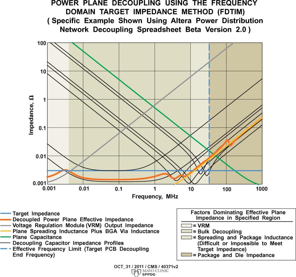
6 SPPDG Archive Motivation Passive Power Distribution Board Frequency Domain Target Impedance Method (FDTIM) dv/di = allowable voltage ripple / expected current transient = target power distribution network (PDN) impedance Z target Championed by Larry Smith (et al.) at Sun in late 1990 s Frequently cited and implemented method for HPC PDN design Z target is frequency-independent (flat across all frequencies) Diverging trends in voltage (decreasing with IC process) and current (increasing with computational requirements) Trending toward the need for sub-milliohm PDN impedance; Z target Fundamental question: What is the lowest practical PCB PDN impedance achievable, over what frequency range, given reasonable technology constraints?
7 Peak Current, A Voltage, V Target Impedance, mohm TRENDS IN PROCESSOR VOLTAGE, PEAK CURRENT AND RESULTING POWER DISTRIBUTION NETWORK TARGET IMPEDANCE Vdd Peak Current [1] Vdd Voltage [2] Target Impedance: 5% Vtol., 50% ΔI Target Impedance: 3% Vtol., 70% ΔI Time, Year [1] Stanley-Marbell, P., Cabezas, V.C., and Luijten, R.P., "Pinned to the Walls - Impact of Packaging and Application Properties on the Memory and Power Walls," International Symposium on Low Power Electronics and Design, pp , August [2] International Technology Roadmap for Semiconductors (ITRS): Executive Summary, 2011 Edition, JUL_31 / 2012 / CMS / 43526
8
9 SPPDG Archive Agenda Introduction to High Performance Compute (HPC) systems Motivation for Printed Circuit Board (PCB) passive power delivery study Design and layout of hypothetical compute PCB State of the art technologies Simulation methodology and results Technology tradeoffs and impact PCB fabrication and measurement Conclusive remarks and future guidance
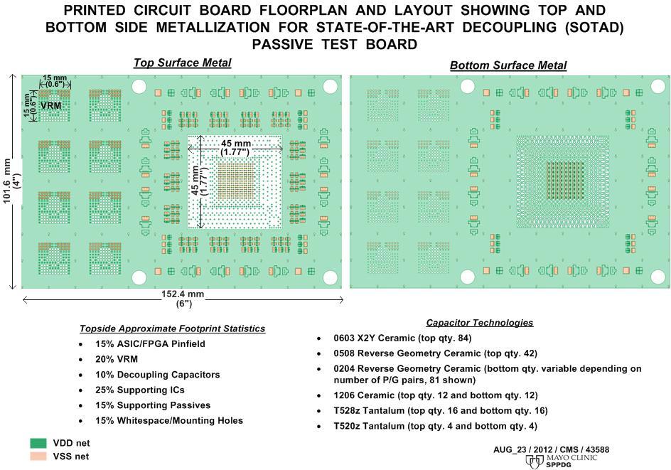
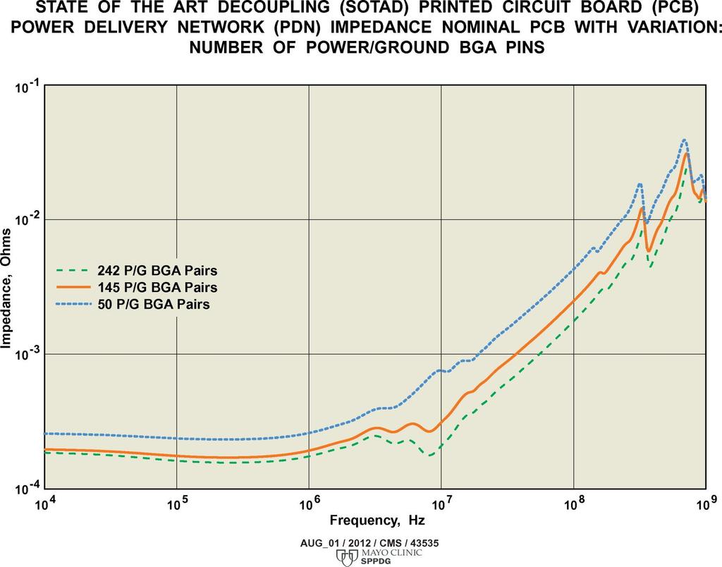
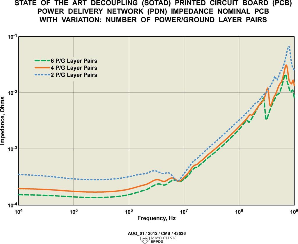
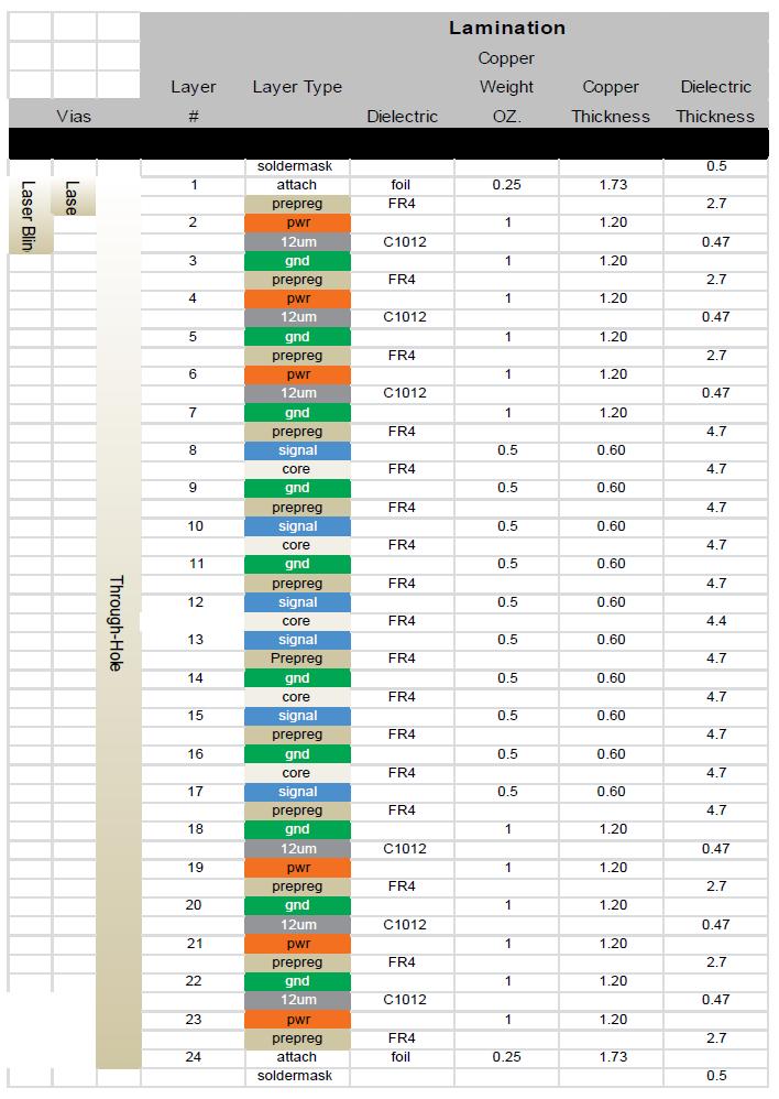
10 Design Passive Power Distribution PCB (1) Elements emulating typical processor PCB in HPC system ASIC/FPGA pinfield 45 mm x 45 mm, 1 mm pin pitch, variable number of P/G pin pairs 50, 145* or 242 Voltage regulation Quantity 8, 15 mm x 15 mm Linear Technology µmodule footprints, populated with copper shorting slugs Provisioned space for auxiliary circuits (memory, passives, etc. and mechanical) Stackup and material sets Reduced spreading inductance with variable ultra-thin dielectrics for P/G plane layers (4, 6, 12*, 14 and 50 µm) Fixed 24 total metal layers, variable P/G layer pairs (2, 4* or 6) Variable P/G copper weight (1* or 2 oz.) Variable total PCB thickness (80, 100* or 120 mils) * Denotes nominal value SPPDG Archive
11 Design Passive Power Distribution PCB (2) Signal vias included to emulate typical P/G plane voiding Oval antipads for differential pairs 10 mil drill, 20 mil pad, 27 mil P/G anti-pad, 32 mil signal anti-pad Pushed technology limits of PCB fabrication vendor State of the art, commercially available decoupling capacitor technology Minimize total loop inductance for highest-frequency performance Low intrinsic self inductance, multi-terminal and reverse-geometry capacitor technology Optimized via design using via-in-pad, for low mounted inductance Highest-frequency capacitors placed nearest to the ASIC/FPGA Variable total quantity (0, 210, 271* or 311) * Denotes nominal value SPPDG Archive
12
13 SPPDG Archive Agenda Introduction to High Performance Compute (HPC) systems Motivation for Printed Circuit Board (PCB) passive power delivery study Design and layout of hypothetical compute PCB State of the art technologies Simulation methodology and results Technology tradeoffs and impact PCB fabrication and measurement Conclusive remarks and future guidance
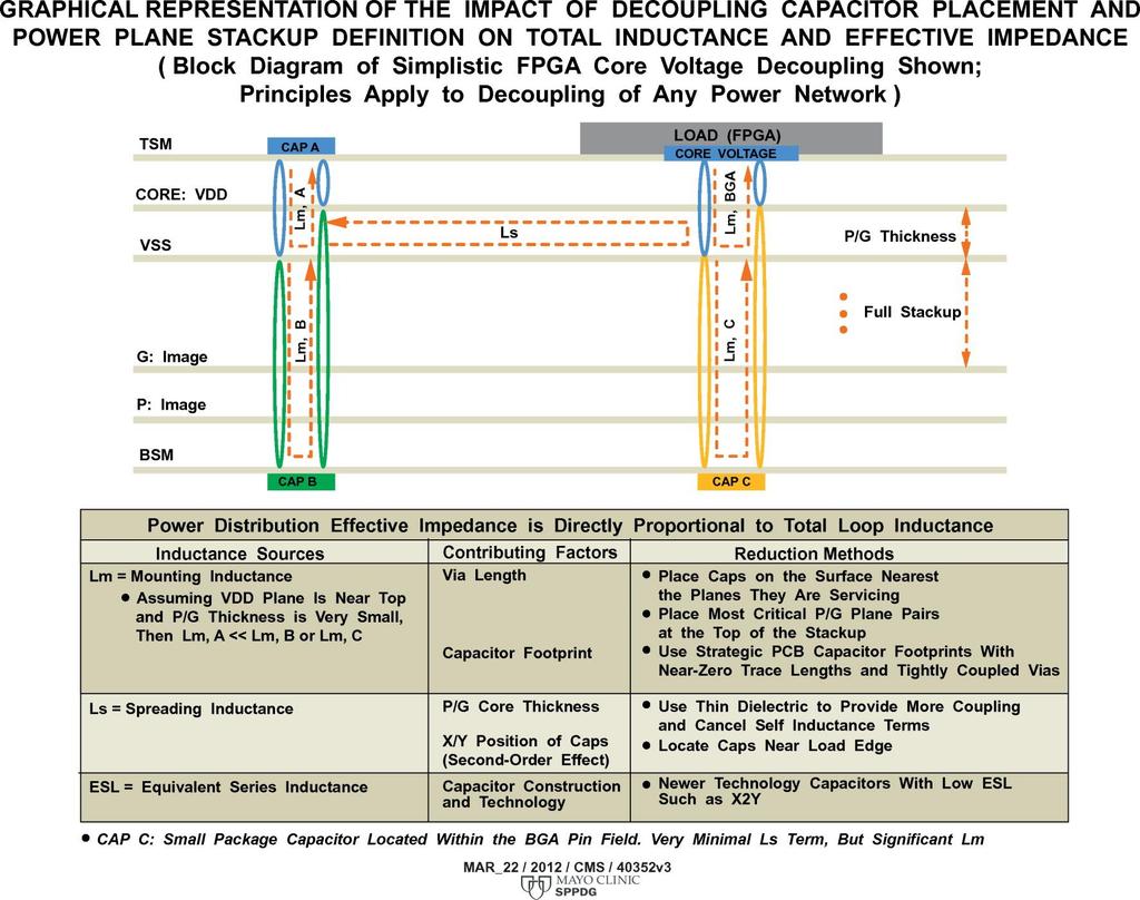
14 SPPDG Archive Simulation Metrics and Methodology Traditional PCB PDN Z(f) curve V-shaped capacitive at low frequency, inductive at high frequency Perfect short at the VRM sites resembles a series resistor and inductor (R/L) circuit Multi-step and multi-tool simulation process used to extract the effective R and L values from the Z(f) curves for a variety of PCB configurations PCB physical layout imported into 2.5D electromagnetic solver Super-port placed on all top-side ASIC/FPGA power/ground pins Frequency noted where Z(f) exceeds 1 mω Low frequency impedance recorded in flat region Inductance calculated in well-behaved, linear region
15
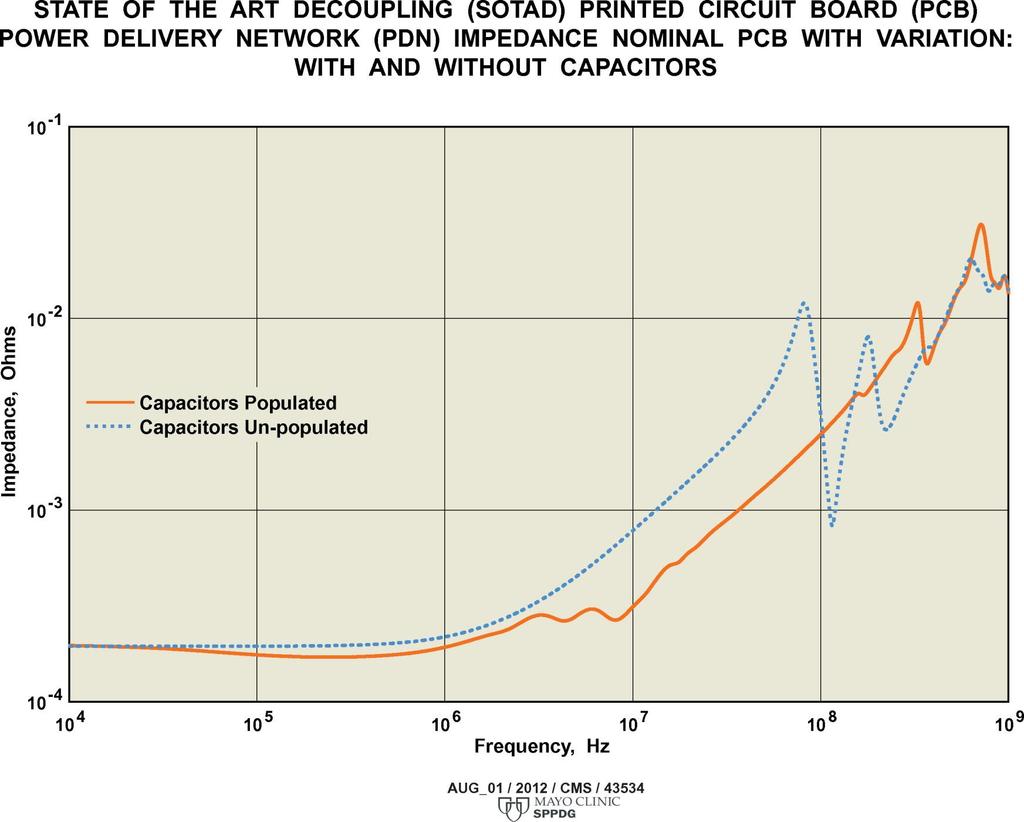
16 SPPDG Archive Simulation Relative Improvement Summary PCB Variation Relative Improvement (Ratio) Low Freq. Z Inductance 1 mω Freq. With caps vs. without caps vs. 242 P/G pin pairs vs. 6 P/G layer pairs um vs um P/G dielectric thickness oz. vs. 2 oz. planar copper weight mil vs. 120 mil PCB thickness Values near 1.00 indicate very little change between test cases e.g. as expected, dielectric thickness had no impact on low frequency Z Results are interdependent on other factors e.g. careful stackup design, with P/G planes near surface, influences relative improvement observed with the addition of capacitors
17 SPPDG Archive Agenda Introduction to High Performance Compute (HPC) systems Motivation for Printed Circuit Board (PCB) passive power delivery study Design and layout of hypothetical compute PCB State of the art technologies Simulation methodology and results Technology tradeoffs and impact PCB fabrication and measurement Conclusive remarks and future guidance
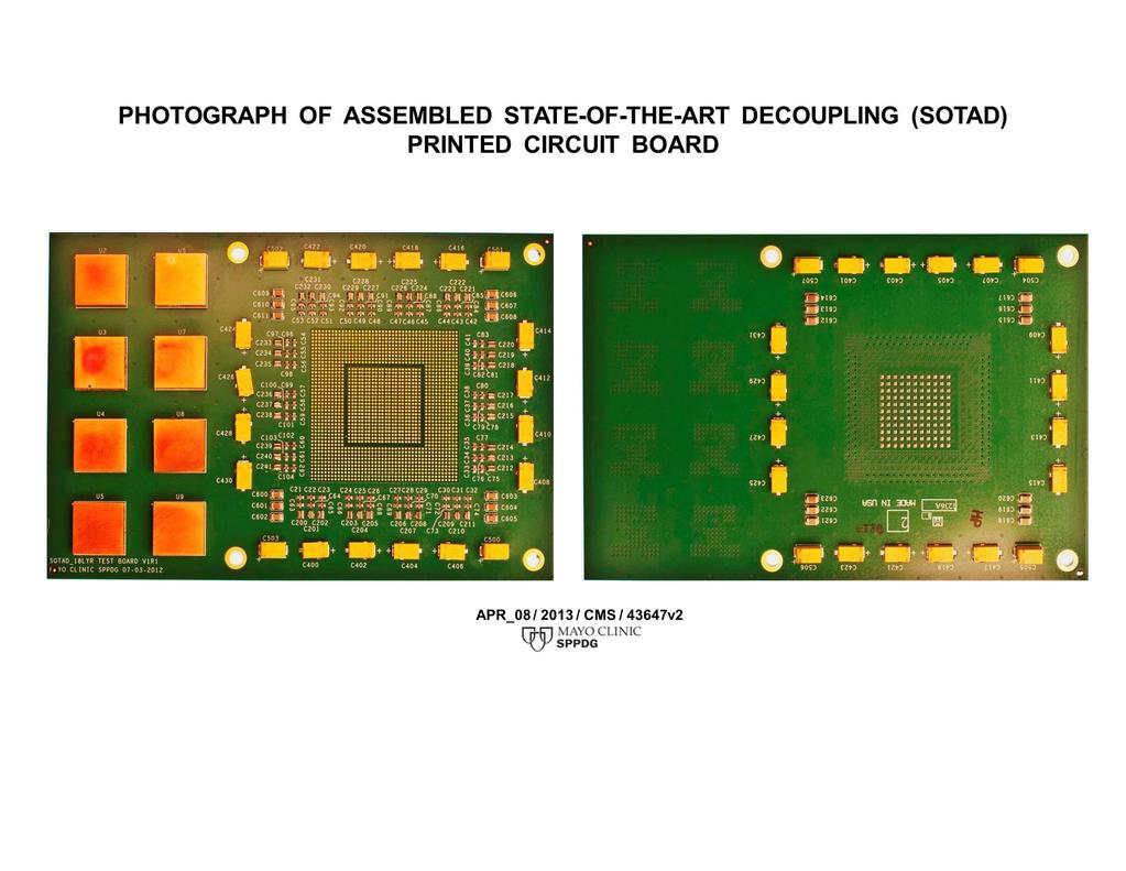
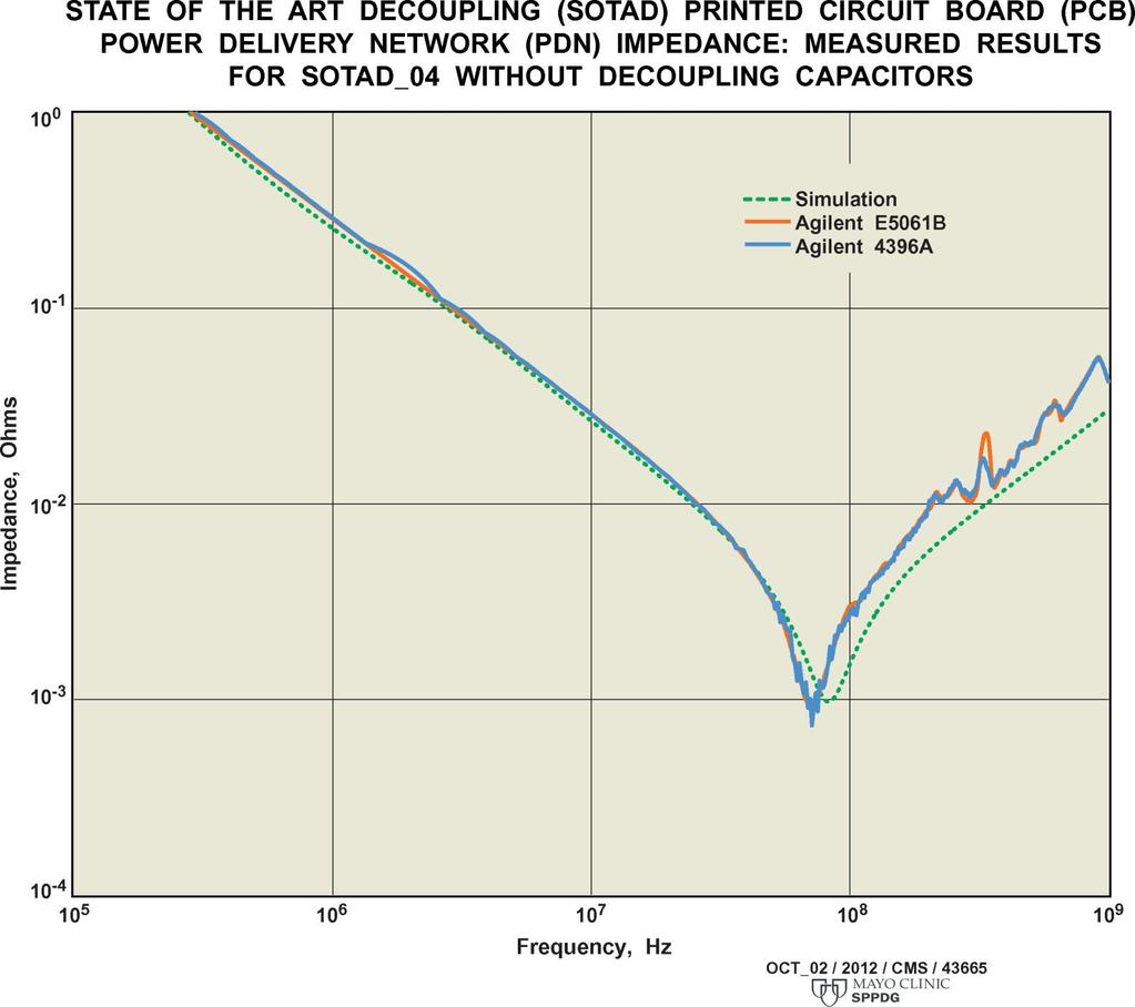
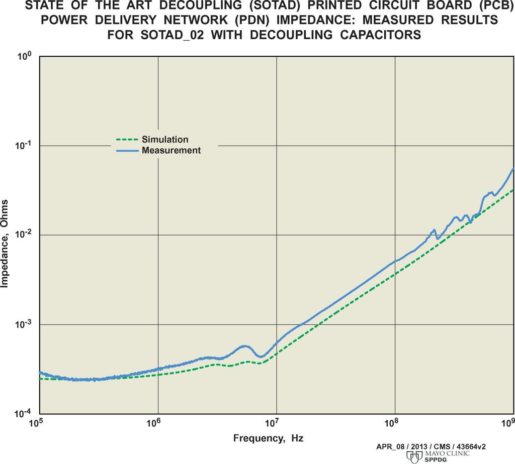
18 SPPDG Archive Fabrication and Measurement Methodology Fabricated practical PCB attributes based on: sensitivity analysis, fabricator guidance, cost and manufacturability 242 P/G pin pairs, 100 mil thick, 311 caps, 1 oz. copper, 6 P/G plane pairs, 12 µm dielectric Assembled in-house with vapor phase solder reflow technology Significant copper in the board created solder reflow and rework challenges recommend optimizing temperature soak / ramp profile Shunt 2-Port VNA measurement methodology [1] High-frequency micro probes applied to pads in ASIC/IC pin field Extract 2-port S-parameters and calculate self-impedance Z(f) Measured with and without shorting slugs attached to VRM pads [1] Agilent, Appl. Note EN, Ultra-Low Impedance Measurements Using 2-Port Measurements, February 2007
19
20
21
22 SPPDG Archive Measurement Results Summary Reasonable measurement correlation to simulation results using equivalent 2-port method High-resolution images of PCB cross-section helped fine-tune the model geometries Low-frequency region (appearing capacitive when VRM shorts are not present, resistive with shorts attached) nearly identical to simulation Elements influencing intrinsic-capacitance and resistance were modeled with great accuracy Minimal discrepancy in modeled vs. measured inductance resulting in differences with the self resonant frequency and high-frequency impedance visible in measurements with and without decoupling capacitors Does not negatively influence report conclusions
23 SPPDG Archive Agenda Introduction to High Performance Compute (HPC) systems Motivation for Printed Circuit Board (PCB) passive power delivery study Design and layout of hypothetical compute PCB State of the art technologies Simulation methodology and results Technology tradeoffs and impact PCB fabrication and measurement Conclusive remarks and future guidance
24 SPPDG Archive Conclusions and Future Direction (1) What is the lowest practical PCB PDN impedance achievable, over what frequency range, given reasonable technology constraints? Low frequency (less than ~1 MHz): µω VRM, DC resistance, copper weight, plane count, bulk decoupling Mid frequency (~ 1 MHz 10 MHz): µω Vias, mid-range capacitor selection and placement, stackup High frequency (> 10 MHz): Increasing proportionally with frequency Vias, capacitor technology and placement, plane location, dielectrics Relying on package and chip decoupling for impedance reduction
25 SPPDG Archive Conclusions and Future Direction (2) Need for frequency-dependent target impedance based on predictable (or partially-predictable) load transients Seeing some progress in recent publications DesignCon, IEEE, etc. Prevent over- or under-design
26 SPPDG Archive THANK YOU! Practical Limitations of State of the Art Passive Printed Circuit Board Power Delivery Networks for High Performance Compute Systems Chad Smutzer 17 th IEEE Workshop on Signal and Power Integrity (SPI) May 14, 2013
27 SPPDG Archive Backup Slides
28
29
30
31
32
33
34
35
The Inductance Loop Power Distribution in the Semiconductor Test Interface. Jason Mroczkowski Multitest
 The Inductance Loop Power Distribution in the Semiconductor Test Interface Jason Mroczkowski Multitest j.mroczkowski@multitest.com Silicon Valley Test Conference 2010 1 Agenda Introduction to Power Delivery
Design, Modeling and Characterization of Embedded Capacitor Networks for Mid-frequency Decoupling in Semiconductor Systems
 Design, Modeling and Characterization of Embedded Capacitor Networks for Mid-frequency Decoupling in Semiconductor Systems Prathap Muthana, Madhavan Swaminathan, Rao Tummala, P.Markondeya Raj, Ege Engin,Lixi
Design of the Power Delivery System for Next Generation Gigahertz Packages
 Design of the Power Delivery System for Next Generation Gigahertz Packages Madhavan Swaminathan Professor School of Electrical and Computer Engg. Packaging Research Center madhavan.swaminathan@ece.gatech.edu
DesignCon Effect of Power Plane Inductance on Power Delivery Networks. Shirin Farrahi, Cadence Design Systems
 DesignCon 2019 Effect of Power Plane Inductance on Power Delivery Networks Shirin Farrahi, Cadence Design Systems shirinf@cadence.com, 978-262-6008 Ethan Koether, Oracle Corp ethan.koether@oracle.com Mehdi
Power Distribution Network Design for Stratix IV GX and Arria II GX FPGAs
 Power Distribution Network Design for Stratix IV GX and Arria II GX FPGAs Transceiver Portfolio Workshops 2009 Question What is Your PDN Design Methodology? Easy Complex Historical Full SPICE simulation
Intro. to PDN Planning PCB Stackup Technology Series
 Introduction to Power Distribution Network (PDN) Planning Bill Hargin In-Circuit Design b.hargin@icd.com.au 425-301-4425 Intro. to PDN Planning 1. Intro/Overview 2. Bypass/Decoupling Strategy 3. Plane
PDN Probes. P2100A/P2101A Data Sheet. 1-Port and 2-Port 50 ohm Passive Probes
 P2100A/P2101A Data Sheet PDN Probes 1-Port and 2-Port 50 ohm Passive Probes power integrity PDN impedance testing ripple PCB resonances transient step load stability and NISM noise TDT/TDR clock jitter
ANSYS CPS SOLUTION FOR SIGNAL AND POWER INTEGRITY
 ANSYS CPS SOLUTION FOR SIGNAL AND POWER INTEGRITY Rémy FERNANDES Lead Application Engineer ANSYS 1 2018 ANSYS, Inc. February 2, 2018 ANSYS ANSYS - Engineering simulation software leader Our industry reach
Understanding, measuring, and reducing output noise in DC/DC switching regulators
 Understanding, measuring, and reducing output noise in DC/DC switching regulators Practical tips for output noise reduction Katelyn Wiggenhorn, Applications Engineer, Buck Switching Regulators Robert Blattner,
PI3DPX1207B Layout Guideline. Table of Contents. 1 Layout Design Guideline Power and GROUND High-speed Signal Routing...
 PI3DPX1207B Layout Guideline Table of Contents 1 Layout Design Guideline... 2 1.1 Power and GROUND... 2 1.2 High-speed Signal Routing... 3 2 PI3DPX1207B EVB layout... 8 3 Related Reference... 8 Page 1
Chapter 16 PCB Layout and Stackup
 Chapter 16 PCB Layout and Stackup Electromagnetic Compatibility Engineering by Henry W. Ott Foreword The PCB represents the physical implementation of the schematic. The proper design and layout of a printed
Frequency-Domain Characterization of Power Distribution Networks
 Frequency-Domain Characterization of Power Distribution Networks Istvan Novak Jason R. Miller ARTECH H O U S E BOSTON LONDON artechhouse.com Preface Acknowledgments xi xv CHAPTER 1 Introduction 1 1.1 Evolution
Thank you for downloading one of our ANSYS whitepapers we hope you enjoy it.
 Thank you! Thank you for downloading one of our ANSYS whitepapers we hope you enjoy it. Have questions? Need more information? Please don t hesitate to contact us! We have plenty more where this came from.
Interconnect-Power Dissipation in a Microprocessor
 4/2/2004 Interconnect-Power Dissipation in a Microprocessor N. Magen, A. Kolodny, U. Weiser, N. Shamir Intel corporation Technion - Israel Institute of Technology 4/2/2004 2 Interconnect-Power Definition
Hardware Design Considerations for MKW41Z/31Z/21Z BLE and IEEE Device
 NXP Semiconductors Document Number: AN5377 Application Note Rev. 2, Hardware Design Considerations for MKW41Z/31Z/21Z BLE and IEEE 802.15.4 Device 1. Introduction This application note describes Printed
Signal Integrity Design of TSV-Based 3D IC
 Signal Integrity Design of TSV-Based 3D IC October 24, 21 Joungho Kim at KAIST joungho@ee.kaist.ac.kr http://tera.kaist.ac.kr 1 Contents 1) Driving Forces of TSV based 3D IC 2) Signal Integrity Issues
Broadband Methodology for Power Distribution System Analysis of Chip, Package and Board for High Speed IO Design
 DesignCon 2009 Broadband Methodology for Power Distribution System Analysis of Chip, Package and Board for High Speed IO Design Hsing-Chou Hsu, VIA Technologies jimmyhsu@via.com.tw Jack Lin, Sigrity Inc.
Application Note 5499
 MGA-31389 and MGA-31489 High-Gain Driver Amplifier Using Avago MGA-31389 and MGA-31489 Application Note 5499 Introduction The MGA-31389 and MGA-31489 from Avago Technologies are.1 Watt flat-gain driver
A Solution to Simplify 60A Multiphase Designs By John Lambert & Chris Bull, International Rectifier, USA
 A Solution to Simplify 60A Multiphase Designs By John Lambert & Chris Bull, International Rectifier, USA As presented at PCIM 2001 Today s servers and high-end desktop computer CPUs require peak currents
Measurement and Comparative S21 Performance of Raw and Mounted Decoupling Capacitors
 Measurement and Comparative S21 Performance of Raw and Mounted Decoupling Capacitors Summary Introduction Capacitors All IC power systems require some level of passive decoupling. The ability to accurately
Application Note 5525
 Using the Wafer Scale Packaged Detector in 2 to 6 GHz Applications Application Note 5525 Introduction The is a broadband directional coupler with integrated temperature compensated detector designed for
HMPP-386x Series MiniPak Surface Mount RF PIN Diodes
 HMPP-86x Series MiniPak Surface Mount RF PIN Diodes Data Sheet Description/Applications These ultra-miniature products represent the blending of Avago Technologies proven semiconductor and the latest in
The Design Challenge to Integrate High Performance Organic Packaging into High End ASIC Strategic Space Based Applications.
 The Design Challenge to Integrate High Performance Organic Packaging into High End ASIC Strategic Space Based Applications May 8, 2007 Abstract: The challenge to integrate high-end, build-up organic packaging
Engineering the Power Delivery Network
 C HAPTER 1 Engineering the Power Delivery Network 1.1 What Is the Power Delivery Network (PDN) and Why Should I Care? The power delivery network consists of all the interconnects in the power supply path
Decoupling Capacitance
 Decoupling Capacitance Nitin Bhardwaj ECE492 Department of Electrical and Computer Engineering Agenda Background On-Chip Algorithms for decap sizing and placement Based on noise estimation Decap modeling
surface mount chip capacitor model
 S (db) CAP-PPI-78N- surface mount chip capacitor model Model Features* Broadband validation: DC 4 GHz Equivalent circuit based Substrate scalable:(.9 H/Er 6.5 mil) Part value scalable: (. to pf) Land Pattern
PDN design and analysis methodology in SI&PI codesign
 PDN design and analysis methodology in SI&PI codesign www.huawei.com Asian IBIS Summit, November 9, 2010, Shenzhen China Luo Zipeng (luozipeng@huawei.com) Liu Shuyao (liushuyao@huawei.com) HUAWEI TECHNOLOGIES
PCB Routing Guidelines for Signal Integrity and Power Integrity
 PCB Routing Guidelines for Signal Integrity and Power Integrity Presentation by Chris Heard Orange County chapter meeting November 18, 2015 1 Agenda Insertion Loss 101 PCB Design Guidelines For SI Simulation
Application Note 5012
 MGA-61563 High Performance GaAs MMIC Amplifier Application Note 5012 Application Information The MGA-61563 is a high performance GaAs MMIC amplifier fabricated with Avago Technologies E-pHEMT process and
Power Plane and Decoupling Optimization. Isaac Waldron
 Power Plane and Decoupling Optimization p Isaac Waldron Overview Frequency- and time-domain power distribution system specifications Decoupling design example Bare board Added d capacitors Buried Capacitance
doi: info:doi/ /icpe
 doi: info:doi/0.09/cpe.205.76825 New Measurement Base De-embedded Load Model for Power Delivery Network Design Motochika Okano,2, Koji Watanabe 3, Masamichi Naitoh, and chiro Omura Kyushu nstitute of Technology,
Modelling electromagnetic field coupling from an ESD gun to an IC
 Modelling electromagnetic field coupling from an ESD gun to an IC Ji Zhang #1, Daryl G Beetner #2, Richard Moseley *3, Scott Herrin *4 and David Pommerenke #5 # EMC Laboratory, Missouri University of Science
Development and Validation of a Microcontroller Model for EMC
 Development and Validation of a Microcontroller Model for EMC Shaohua Li (1), Hemant Bishnoi (1), Jason Whiles (2), Pius Ng (3), Haixiao Weng (2), David Pommerenke (1), and Daryl Beetner (1) (1) EMC lab,
Signal Integrity Modeling and Measurement of TSV in 3D IC
 Signal Integrity Modeling and Measurement of TSV in 3D IC Joungho Kim KAIST joungho@ee.kaist.ac.kr 1 Contents 1) Introduction 2) 2.5D/3D Architectures with TSV and Interposer 3) Signal integrity, Channel
3D integrated POL converter
 3D integrated POL converter Presented by: Arthur Ball I- 1 Motivation for this work Today s typical approach for >15A output Point of Load converters: Use PCB material for the entire circuit layout. Need
Foundry WLSI Technology for Power Management System Integration
 1 Foundry WLSI Technology for Power Management System Integration Chuei-Tang Wang, Chih-Lin Chen, Jeng-Shien Hsieh, Victor C.Y. Chang, Douglas Yu R&D,TSMC Oct. 2016 2 Motivation Outline PMIC system integration
Advanced Topics in EMC Design. Issue 1: The ground plane to split or not to split?
 NEEDS 2006 workshop Advanced Topics in EMC Design Tim Williams Elmac Services C o n s u l t a n c y a n d t r a i n i n g i n e l e c t r o m a g n e t i c c o m p a t i b i l i t y e-mail timw@elmac.co.uk
Application Note 5011
 MGA-62563 High Performance GaAs MMIC Amplifier Application Note 511 Application Information The MGA-62563 is a high performance GaAs MMIC amplifier fabricated with Avago Technologies E-pHEMT process and
RF OUT / N/C RF IN / V G
 MAAM-111 MHz - 2 GHz Rev. V2 Features Functional Schematic 12 db Gain Ω Input / Output Match over Gain Range 3 db Gain Control with to -2 V Control +18 dbm Output Power + V, -. V DC, 7 ma Lead-Free 1.
2.5D & 3D Package Signal Integrity A Paradigm Shift
 2.5D & 3D Package Signal Integrity A Paradigm Shift Nozad Karim Technology & Platform Development November, 2011 Enabling a Microelectronic World Content Traditional package signal integrity vs. 2.5D/3D
T est POST OFFICE BOX 1927 CUPERTINO, CA TEL E P H ONE (408) FAX (408) ARIES ELECTRONICS
 FAX (408) ARIES ELECTRONICS") G iga T est L abs POST OFFICE BOX 1927 CUPERTINO, CA 95015 TEL E P H ONE (408) 524-2700 FAX (408) 524-2777 ARIES ELECTRONICS BGA SOCKET (0.80MM TEST CENTER PROBE CONTACT) Final Report Electrical Characterization
G iga T est L abs POST OFFICE BOX 1927 CUPERTINO, CA 95015 TEL E P H ONE (408) 524-2700 FAX (408) 524-2777 ARIES ELECTRONICS BGA SOCKET (0.80MM TEST CENTER PROBE CONTACT) Final Report Electrical Characterization
PART MAX2605EUT-T MAX2606EUT-T MAX2607EUT-T MAX2608EUT-T MAX2609EUT-T TOP VIEW IND GND. Maxim Integrated Products 1
 19-1673; Rev 0a; 4/02 EVALUATION KIT MANUAL AVAILABLE 45MHz to 650MHz, Integrated IF General Description The are compact, high-performance intermediate-frequency (IF) voltage-controlled oscillators (VCOs)
surface mount chip capacitor model
 surface mount chip capacitor model Model Features* Broadband validation: DC 30 GHz Equivalent circuit based Applicable for horizontal mounted capacitors Substrate scalable: (1 H/Er 16.7 mil) Part value
CROSSTALK DUE TO PERIODIC PLANE CUTOUTS. Jason R. Miller, Gustavo Blando, Istvan Novak Sun Microsystems
 CROSSTALK DUE TO PERIODIC PLANE CUTOUTS Jason R. Miller, Gustavo Blando, Istvan Novak Sun Microsystems 1 Outline 1 Introduction 2 Crosstalk Theory 3 Measurement 4 Simulation correlation 5 Parameterized
Challenges and More Challenges SW Test Workshop June 9, 2004
 Innovating Test Technologies Challenges and More Challenges SW Test Workshop June 9, 2004 Cascade Microtech Pyramid Probe Division Ken Smith Dean Gahagan Challenges and More Challenges Probe card requirements
The Facts about the Input Impedance of Power and Ground Planes
 The Facts about the Input Impedance of Power and Ground Planes The following diagram shows the power and ground plane structure of which the input impedance is computed. Figure 1. Configuration of the
How to anticipate Signal Integrity Issues: Improve my Channel Simulation by using Electromagnetic based model
 How to anticipate Signal Integrity Issues: Improve my Channel Simulation by using Electromagnetic based model HSD Strategic Intent Provide the industry s premier HSD EDA software. Integration of premier
Vishram S. Pandit, Intel Corporation (916) ]
![Vishram S. Pandit, Intel Corporation (916) ]](/thumbs/72/66540527.jpg "Vishram S. Pandit, Intel Corporation (916) ]") DesignCon 2008 Simulation and Characterization of GHz On-Chip Power Delivery Network (PDN) Vishram S. Pandit, Intel Corporation [vishram.s.pandit@intel.com, (916)356-2059] Woong Hwan Ryu, Intel Corporation
DesignCon 2008 Simulation and Characterization of GHz On-Chip Power Delivery Network (PDN) Vishram S. Pandit, Intel Corporation [vishram.s.pandit@intel.com, (916)356-2059] Woong Hwan Ryu, Intel Corporation
Synthesis of Optimal On-Chip Baluns
 Synthesis of Optimal On-Chip Baluns Sharad Kapur, David E. Long and Robert C. Frye Integrand Software, Inc. Berkeley Heights, New Jersey Yu-Chia Chen, Ming-Hsiang Cho, Huai-Wen Chang, Jun-Hong Ou and Bigchoug
Accurate Simulation of RF Designs Requires Consistent Modeling Techniques
 From September 2002 High Frequency Electronics Copyright 2002, Summit Technical Media, LLC Accurate Simulation of RF Designs Requires Consistent Modeling Techniques By V. Cojocaru, TDK Electronics Ireland
Chip Package - PC Board Co-Design: Applying a Chip Power Model in System Power Integrity Analysis
 Chip Package - PC Board Co-Design: Applying a Chip Power Model in System Power Integrity Analysis Authors: Rick Brooks, Cisco, ricbrook@cisco.com Jane Lim, Cisco, honglim@cisco.com Udupi Harisharan, Cisco,
Learning the Curve BEYOND DESIGN. by Barry Olney
 by Barry Olney coulmn BEYOND DESIGN Learning the Curve Currently, power integrity is just entering the mainstream market phase of the technology adoption life cycle. The early market is dominated by innovators
Guide to CMP-28/32 Simbeor Kit
 Guide to CMP-28/32 Simbeor Kit CMP-28 Rev. 4, Sept. 2014 Simbeor 2013.03, Aug. 10, 2014 Simbeor : Easy-to-Use, Efficient and Cost-Effective Electromagnetic Software Introduction Design of PCB and packaging
FPA Printed Circuit Board Layout Guidelines
 APPLICATION NOTE AN:005 FPA Printed Circuit Board Layout Guidelines Paul Yeaman Principal Product Line Engineer VI Chip Strategic Accounts Contents Page Introduction 1 The Importance of Board Layout 1
System Power Distribution Network Theory and Performance with Various Noise Current Stimuli Including Impacts on Chip Level Timing
 System Power Distribution Network Theory and Performance with Various Noise Current Stimuli Including Impacts on Chip Level Timing Larry Smith, Shishuang Sun, Peter Boyle, Bozidar Krsnik Altera Corp. Abstract-Power
Trends and Challenges in VLSI Technology Scaling Towards 100nm
 Trends and Challenges in VLSI Technology Scaling Towards 100nm Stefan Rusu Intel Corporation stefan.rusu@intel.com September 2001 Stefan Rusu 9/2001 2001 Intel Corp. Page 1 Agenda VLSI Technology Trends
Implementation of Power Transmission Lines to Field Programmable Gate Array ICs for Managing Signal and Power Integrity
 Implementation of Power Transmission Lines to Field Programmable Gate Array ICs for Managing Signal and Power Integrity Sang Kyu Kim, Satyanarayana Telikepalli, Sung Joo Park, Madhavan Swaminathan and
What is New about Thin Laminates in 2013?
 PCBDesign 007 QuietPower column What is New about Thin Laminates in 2013? Istvan Novak, Oracle, February 2013 It is almost two years ago that the QuietPower column Thin Laminates: Buried Capacitance or
Relationship Between Signal Integrity and EMC
 Relationship Between Signal Integrity and EMC Presented by Hasnain Syed Solectron USA, Inc. RTP, North Carolina Email: HasnainSyed@solectron.com 06/05/2007 Hasnain Syed 1 What is Signal Integrity (SI)?
Application of Generalized Scattering Matrix for Prediction of Power Supply Noise
 Application of Generalized Scattering Matrix for Prediction of Power Supply Noise System Level Interconnect Prediction 2010 June 13, 2010 K. Yamanaga (1),K. Masu (2), and T. Sato (3) (1) Murata Manufacturing
Power Delivery Network (PDN) Tool
 Tool") Power Delivery Network (PDN) Tool User Guide 101 Innovation Drive San Jose, CA 95134 http://www.altera.com Document Version: 1.0 Document Date: UG-01036-1.0 101 Innovation Drive San Jose, CA 95134 www.altera.com
Power Delivery Network (PDN) Tool User Guide 101 Innovation Drive San Jose, CA 95134 http://www.altera.com Document Version: 1.0 Document Date: UG-01036-1.0 101 Innovation Drive San Jose, CA 95134 www.altera.com
Class-D Audio Power Amplifiers: PCB Layout For Audio Quality, EMC & Thermal Success (Home Entertainment Devices)
") Class-D Audio Power Amplifiers: PCB Layout For Audio Quality, EMC & Thermal Success (Home Entertainment Devices) Stephen Crump http://e2e.ti.com Audio Power Amplifier Applications Audio and Imaging Products
Class-D Audio Power Amplifiers: PCB Layout For Audio Quality, EMC & Thermal Success (Home Entertainment Devices) Stephen Crump http://e2e.ti.com Audio Power Amplifier Applications Audio and Imaging Products
Impact of On-Chip Multi-Layered Inductor on Signal and Power Integrity of Underlying Power-Ground Net
 22 nd IEEE Workshop on Signal and Power Integrity, Brest, FRANCE May 25, 2018 Impact of On-Chip Multi-Layered Inductor on Signal and Power Integrity of Underlying Power-Ground Net Akira Tsuchicya 1, Akitaka
Design and Demonstration of a Passive, Broadband Equalizer for an SLED Chris Brinton, Matthew Wharton, and Allen Katz
 Introduction Design and Demonstration of a Passive, Broadband Equalizer for an SLED Chris Brinton, Matthew Wharton, and Allen Katz Wavelength Division Multiplexing Passive Optical Networks (WDM PONs) have
MPC 5534 Case study. E. Sicard (1), B. Vrignon (2) Toulouse France. Contact : web site :
, B. Vrignon (2) Toulouse France. Contact : web site :") MPC 5534 Case study E. Sicard (1), B. Vrignon (2) (1) INSA-GEI, 135 Av de Rangueil 31077 Toulouse France (2) Freescale Semiconductors, Toulouse, France Contact : etienne.sicard@insa-toulouse.fr web site
MPC 5534 Case study E. Sicard (1), B. Vrignon (2) (1) INSA-GEI, 135 Av de Rangueil 31077 Toulouse France (2) Freescale Semiconductors, Toulouse, France Contact : etienne.sicard@insa-toulouse.fr web site
DesignCon Full Chip Signal and Power Integrity with Silicon Substrate Effect. Norio Matsui Dileep Divekar Neven Orhanovic
 DesignCon 2004 Chip-Level Physical Design Full Chip Signal and Power Integrity with Silicon Substrate Effect Norio Matsui Dileep Divekar Neven Orhanovic Applied Simulation Technology, Inc. 408-436-9070
IC Decoupling and EMI Suppression using X2Y Technology
 IC Decoupling and EMI Suppression using X2Y Technology Summary Decoupling and EMI suppression of ICs is a complex system level engineering problem complicated by the desire for faster switching gates,
High Speed Design Issues and Jitter Estimation Techniques. Jai Narayan Tripathi
 High Speed Design Issues and Jitter Estimation Techniques Jai Narayan Tripathi (jainarayan.tripathi@st.com) Outline Part 1 High-speed Design Issues Signal Integrity Power Integrity Jitter Power Delivery
Performance Improvement by System Aware Substrate Noise Analysis for Mixed-signal IC
 DesignCon 2017 Performance Improvement by System Aware Substrate Noise Analysis for Mixed-signal IC Kwangseok Choi, Samsung Electronics Inc. [aquarian505@gmail.com] Byunghyun Lee, Samsung Electronics Inc.
Manufacture and Performance of a Z-interconnect HDI Circuit Card Abstract Introduction
 Manufacture and Performance of a Z-interconnect HDI Circuit Card Michael Rowlands, Rabindra Das, John Lauffer, Voya Markovich EI (Endicott Interconnect Technologies) 1093 Clark Street, Endicott, NY 13760
Best Design and Layout Practices for SiTime Oscillators
 March 17, 2016 Best Design and Layout Practices 1 Introduction... 1 2 Decoupling... 1 3 Bypassing... 4 4 Power Supply Noise Reduction... 5 5 Power Supply Management... 6 6 Layout Recommendations for SiTime
Basic Concepts C HAPTER 1
 C HAPTER 1 Basic Concepts Power delivery is a major challenge in present-day systems. This challenge is expected to increase in the next decade as systems become smaller and new materials are introduced
Optimization of Wafer Level Test Hardware using Signal Integrity Simulation
 June 7-10, 2009 San Diego, CA Optimization of Wafer Level Test Hardware using Signal Integrity Simulation Jason Mroczkowski Ryan Satrom Agenda Industry Drivers Wafer Scale Test Interface Simulation Simulation
Measurement of Laddering Wave in Lossy Serpentine Delay Line
 International Journal of Applied Science and Engineering 2006.4, 3: 291-295 Measurement of Laddering Wave in Lossy Serpentine Delay Line Fang-Lin Chao * Department of industrial Design, Chaoyang University
Signal Integrity Modeling and Simulation for IC/Package Co-Design
 Signal Integrity Modeling and Simulation for IC/Package Co-Design Ching-Chao Huang Optimal Corp. October 24, 2004 Why IC and package co-design? The same IC in different packages may not work Package is
Effect of Power Distribution Network Design on RF circuit performance for 900MHz RFID Reader
 Effect of Power Distribution Network Design on RF circuit performance for 900MHz RFID Reader Youngwon Kim, Chunghyun Ryu, Jongbae Park, and Joungho Kim Terahertz Interconnection and Package Laboratory,
nan Small loop antennas APPLICATION NOTE 1. General 2. Loop antenna basics
 nan400-03 1. General For F designers developing low-power radio devices for short-range applications, antenna design has become an important issue for the total radio system design. Taking the demand for
Electromagnetic Analysis of AC Coupling Capacitor Mounting Structures
 Simbeor Application Note #2008_02, April 2008 2008 Simberian Inc. Electromagnetic Analysis of AC Coupling Capacitor Mounting Structures Simberian, Inc. www.simberian.com Simbeor : Easy-to-Use, Efficient
Automotive PCB SI and PI analysis
 Automotive PCB SI and PI analysis SI PI Analysis Signal Integrity S-Parameter Timing analysis Eye diagram Power Integrity Loop / Partial inductance DC IR-Drop AC PDN Impedance Power Aware SI Signal Integrity
Characterization Methodology for High Density Microwave Fixtures. Dr. Brock J. LaMeres, Montana State University
 DesignCon 2008 Characterization Methodology for High Density Microwave Fixtures Dr. Brock J. LaMeres, Montana State University lameres@ece.montana.edu Brent Holcombe, Probing Technology, Inc brent.holcombe@probingtechnology.com
Wideband On-die Power Supply Decoupling in High Performance DRAM
 Wideband On-die Power Supply Decoupling in High Performance DRAM Timothy M. Hollis, Senior Member of the Technical Staff Abstract: An on-die decoupling scheme, enabled by memory array cell technology,
Surface Mount RF PIN Low Distortion Attenuator Diodes. Technical Data. HSMP-381x Series and HSMP-481x Series. Features
 Surface Mount RF PIN Low Distortion Attenuator Diodes Technical Data HSMP-81x Series and HSMP-481x Series Features Diodes Optimized for: Low Distortion Attenuating Microwave Frequency Operation Surface
Measurement Results for a High Throughput MCM
 Measurement Results for a High Throughput MCM Funding: Paul Franzon Toby Schaffer, Alan Glaser, Steve Lipa North Carolina State University paulf@ncsu.edu www.ece.ncsu.edu/erl Outline > Heterogeneous System
CIRCUITS. Raj Nair Donald Bennett PRENTICE HALL
 POWER INTEGRITY ANALYSIS AND MANAGEMENT I CIRCUITS Raj Nair Donald Bennett PRENTICE HALL Upper Saddle River, NJ Boston Indianapolis San Francisco New York Toronto Montreal London Munich Paris Madrid Capetown
Research in Support of the Die / Package Interface
 Research in Support of the Die / Package Interface Introduction As the microelectronics industry continues to scale down CMOS in accordance with Moore s Law and the ITRS roadmap, the minimum feature size
PDS Impact for DDR Low Cost Design
 PDS Impact for DDR3-1600 Low Cost Design Jack W.C. Lin Sr. AE Manager jackl@cadence.com Aug. g 13 2013 Cadence, OrCAD, Allegro, Sigrity and the Cadence logo are trademarks of Cadence Design Systems, Inc.
Simulation and Design of Printed Circuit Boards Utilizing Novel Embedded Capacitance Material
 Simulation and Design of Printed Circuit Boards Utilizing Novel Embedded Capacitance Material April 28, 2010 Yu Xuequan, Yanhang, Zhang Gezi, Wang Haisan Huawei Technologies CO., LTD. Shanghai, China Tony_yu@huawei.com
Reliable World Class Insights Your Silicon Valley Partner in Simulation ANSYS Sales, Consulting, Training & Support
 www.ozeninc.com info@ozeninc.com (408) 732 4665 1210 E Arques Ave St 207 Sunnyvale, CA 94085 Reliable World Class Insights Your Silicon Valley Partner in Simulation ANSYS Sales, Consulting, Training &
Microcircuit Electrical Issues
 Microcircuit Electrical Issues Distortion The frequency at which transmitted power has dropped to 50 percent of the injected power is called the "3 db" point and is used to define the bandwidth of the
POWER designer Expert tips, tricks, and techniques for powerful designs
 POWER designer Expert tips, tricks, and techniques for powerful designs No. 114 Feature Article...1-7 High Power Density Regulators...2 Best Layout Practices for Switching Power Supplies By L. Haachitaba
RFPA5542 WLAN POWER AMPLIFIER 5 GHz WLAN PA (11a/n/ac)
") RFPA5542 WLAN POWER AMPLIFIER 5 GHz WLAN PA (11a/n/ac) Introduction This application note explains the operation of the RFPA5542 5GHz WLAN PA. The RFPA5542 is a three-stage power amplifier (PA) designed
RFPA5542 WLAN POWER AMPLIFIER 5 GHz WLAN PA (11a/n/ac) Introduction This application note explains the operation of the RFPA5542 5GHz WLAN PA. The RFPA5542 is a three-stage power amplifier (PA) designed
1 FUNDAMENTAL CONCEPTS What is Noise Coupling 1
 Contents 1 FUNDAMENTAL CONCEPTS 1 1.1 What is Noise Coupling 1 1.2 Resistance 3 1.2.1 Resistivity and Resistance 3 1.2.2 Wire Resistance 4 1.2.3 Sheet Resistance 5 1.2.4 Skin Effect 6 1.2.5 Resistance
Practical Design Considerations for Dense, High-Speed, Differential Stripline PCB Routing Related to Bends, Meanders and Jog-outs
 Practical Design Considerations for Dense, High-Speed, Differential Stripline PCB Routing Related to Bends, Meanders and Jog-outs AUTHORS Michael J. Degerstrom, Mayo Clinic degerstrom.michael@mayo.edu
PAGE 1/6 ISSUE Jul SERIES Micro-SPDT PART NUMBER R516 XXX 10X R 516 _ 1 0 _
 PAGE 1/6 ISSUE Jul-24-2017 SERIES Micro-SPDT PART NUMBER R516 XXX 10X R516 series: the RAMSES concept merges with the SLIM LINE technology, breaking up the frequency limits of SMT switches : - FULL SMT
SSO Noise, Eye Margin, and Jitter Characterization for I/O Power Integrity
 DESIGNCON 2009 SSO Noise, Eye Margin, and Jitter Characterization for I/O Power Integrity Vishram S. Pandit, Intel Corporation [vishram.s.pandit@intel.com, (916)356-2059] Ashish N. Pardiwala, Intel Corporation
A Simulation Study of Simultaneous Switching Noise
 A Simulation Study of Simultaneous Switching Noise Chi-Te Chen 1, Jin Zhao 2, Qinglun Chen 1 1 Intel Corporation Network Communication Group, LOC4/19, 9750 Goethe Road, Sacramento, CA 95827 Tel: 916-854-1178,
EMI. Chris Herrick. Applications Engineer
 Fundamentals of EMI Chris Herrick Ansoft Applications Engineer Three Basic Elements of EMC Conduction Coupling process EMI source Emission Space & Field Conductive Capacitive Inductive Radiative Low, Middle
EL7302. Hardware Design Guide
 Hardware Design Guide Version: Preliminary 0.0 Date: January. 2005 Approval: Etron technology, Inc P.O. Box 19-54 No.6 Technology Road V. Science-based Industrial Park, Hsinchu,30077 Taiwan, R.O.C. Tel:
Silicon Interposers enable high performance capacitors
 Interposers between ICs and package substrates that contain thin film capacitors have been used previously in order to improve circuit performance. However, with the interconnect inductance due to wire
AltiumLive 2017: Component selection for EMC
 AltiumLive 2017: Component selection for EMC Martin O Hara Victory Lighting Ltd Munich, 24-25 October 2017 Component Selection Passives resistors, capacitors and inductors Discrete diodes, bipolar transistors,