Chapter 16 PCB Layout and Stackup
|
|
|
- Joel Collins
- 6 years ago
- Views:
Transcription
1 Chapter 16 PCB Layout and Stackup Electromagnetic Compatibility Engineering by Henry W. Ott
2 Foreword The PCB represents the physical implementation of the schematic. The proper design and layout of a printed circuit board can mean the difference between the product passing or failing EMC requirements. Such things as component placement, keep out zones, trace routing, number of layers, layer stackup (order of layers and layer spacing), and return path discontinuities all are critical to the EMC performance of the board. 2
3 General PCB Layout Considerations - Partitioning Components should be grouped into logical functional blocks. Some of these blocks might be: (1) high-speed logic, clocks, and clock drivers; (2) memory; (3) medium- and low-speed logic; (4) video; (5) audio and other low-frequency analog circuits; (6) input/output (I/O) drivers; and (7) I/O connectors and common-mode filters 3
4 General PCB Layout Considerations - Partitioning 4
5 General PCB Layout Considerations - Partitioning On a properly partitioned board, the high-speed logic as well as memory should not be located near the I/O area. The crystal or high-frequency oscillator should be located near the integrated circuits (ICs) that use them, and away from the I/O area of the board. The I/O drivers should be located close to the connectors. The video and low-frequency analog circuits should have access to the I/O area without having to pass through the high-frequency digital sections of the board. Proper partitioning will minimize trace lengths, improve signal quality, minimize parasitic coupling, and reduce both PCB emissions and susceptibility. 5
6 General PCB Layout Considerations Keep Out Zones Be particularly careful to keep the oscillators and/or crystals, as well as any other high-frequency circuitry, away from the I/O area. These circuits generate high-frequency fields (both electric and magnetic) that can easily couple directly to the I/O cables, connectors, and circuitry. Experience has shown, that if board size permits, keeping these circuits at least 0.5 in. (13 mm) from the I/O area will minimize the parasitic coupling. Route all critical signal traces away from the edges of the board to allow the return current to spread out under the trace. A good rule is to define a keep out zone, that is 20 times the signal-layer to return-plane spacing, around the periphery of the board. 6

7 General PCB Layout Considerations Keep Out Zones 7
8 General PCB Layout Considerations Critical Signals Experience has shown that 90% of PCB problems are caused by 10% of the circuitry. For emissions, the greatest problems are high-frequency (fast rise time) digital circuits with repetitive wave shapes, such as clocks, buses, and some control signals. These signals contain a multiplicity of large-amplitude, high-frequency harmonics. Clocks are usually the worst offenders, followed in order by buses and then repetitive control signals. An effective metric for categorizing signal speed (in A/s 2 ) is 8
9 General PCB Layout Considerations System Clocks Keep the clock traces as short as possible and provide for optimum placement by routing them first. Locate crystals, oscillators, or resonators as close to the circuits that use them as possible. Add a ground plane on the component side of the board under the crystal, oscillator, and/or clock driver. Connect this plane to the main ground plane with multiple vias. If the crystal or oscillator has a metal case, ground it to this componentside ground plane, and provide a provision for a board level shield over this area in case it should be needed. Small series damping resistors (or ferrite beads) should be added to all clock output traces with a frequency of 20 MHz or more. 9
10 General PCB Layout Considerations System Clocks This is recommended even on short clock traces, unless adding the resistor would increase the length of an already very short trace. A typical value resistor would be 33. Clock oscillators and drivers should also have ferrite beads in series with the V cc line to isolate the circuit from the main power distribution system. 10
11 PCB-to-Chassis Ground Connection A major source of radiation from electronic products is due to commonmode currents on the external cables. The internal circuit ground should be connected to the chassis at a point as close to the location that the cables terminate on the PCB as possible. The connection should be short, and there should be multiple connections to parallel the inductance of the connections, and, hence, decrease the radio frequency (rf) impedance. 11
12 Return Path Discontinuities One of the keys to determining the optimum printed circuit board layout is to understand how and where the signal return currents actually flow. The lowest impedance return path is in a plane directly underneath the signal trace. A plane is really two conductors. Major EMC, and signal integrity (SI), problems occur when there are discontinuities in the return current path. These discontinuities cause the return current to flow in large loops, which increases the ground inductance and the radiation from the board as well as increasing the crosstalk between adjacent traces and causing waveform distortion. 12

13 Return Path Discontinuities In addition, a return plane discontinuity on a constant impedance PCB will change the characteristic impedance of the trace and produce reflections. The three most common return path discontinuities: Slots or splits in the power and/or ground plane Signal traces changing layers, which causes the return currents to change reference planes Ground plane cutouts around connectors, or under ICs Slots in Ground/Power Planes If you must have slots, make sure that no traces cross over them on adjacent layers. 13
 Holes in ground plane.")
14 Return Path Discontinuities Slots in Ground/Power Planes Ground plane slots and/or splits can increase the PCB radiation in excess of 20 db. Fig (B) Holes in ground plane. 14

15 Return Path Discontinuities Split Ground/Power Planes This much larger return current path significantly increases the inductance, and loop area, of the return path. If in the above example, both the power and ground planes are split, then how will the return current get across the gap? The best solution to the split plane problem is to avoid crossing the split with any signal traces, especially critical signal traces. The signal should have been routed on the bottom signal layer adjacent to the solid ground plane. 15
16 Return Path Discontinuities Split Ground/Power Planes Many products today require multiple direct current (dc) voltages to operate. As a result, split power planes are becoming a common occurrence. Five approaches are available for dealing with the problem created by split power planes. Split the power plane and live with the routing restrictions. Use a separate solid power plane for each dc voltage. Use a power island for one or more of the voltages. A power island is a small isolated power plane on a signal layer (usually on the top or bottom layer of the board) under one or more ICs. Route some (or all) of the dc voltages as a trace on a signal layer. As a last resort, add stitching capacitors where the trace crosses the split plane. The power island approach is most useful when a dc voltage is used only by one or more ICs located adjacent to each other. 16
17 Return Path Discontinuities Split Ground/Power Planes Although signal traces should not be run across a split in an adjacent plane, design constraints, and cost considerations, sometimes make it necessary to do so, especially in the case of power planes. The capacitors should be located within 0.1 in. of the trace and have a value of to 0.01 F according to the frequency of the signal. 17
18 Return Path Discontinuities Split Ground/Power Planes This solution is far from a ideal; the return current must now flow through a via, a trace, a mounting pad, a capacitor, a mounting pad, a trace, and finally a via to the other section of the split plane. This adds about 5 nh, or more, of additional inductance (impedance) in the ground return path, but it is better than the alternative of doing nothing. 18

19 Return Path Discontinuities Changing Reference Planes The interplane capacitance is not large enough to provide a low impedance path, so the return current will have to flow through the nearest decoupling capacitor, or plane-to-plane via to change planes. 19
20 Return Path Discontinuities Changing Reference Planes Changing reference planes effectively adds impedance (inductance) in the return path. One solution to this problem is to avoid switching reference planes for critical signals (such as clocks), if at all possible. 20
21 Return Path Discontinuities Changing Reference Planes If you must switch references from a power plane to a ground plane, then you can place an additional decoupling capacitor* adjacent to the signal via to provide a high-frequency current return path between the two planes. This solution is not ideal, however, because this adds considerable additional inductance in the return path (typically about 5 nh). Note that if the two reference planes are of the same type (either both power or both ground), then you can use a plane-to-plane via (groundto-ground, or power-to-power) instead of a capacitor immediately adjacent to the signal via. 21
22 Return Path Discontinuities Changing Reference Planes 22
23 Return Path Discontinuities Referencing the Top and Bottom of the Same Plane To drop a signal via through a plane, a clearance hole (anti-pad) must be provided in the plane; otherwise the signal would be shorted to the reference plane. The inside surface of the clearance hole provides a surface connecting the top and bottom of the plane and provides the path for the return current to flow from the top to the bottom of the plane as depicted in Fig
24 Return Path Discontinuities Referencing the Top and Bottom of the Same Plane High-speed clocks and other critical signals should be routed (in order of preference) as follows: On only one layer adjacent to a plane. On two layers that are adjacent to the same plane. On two layers adjacent to two separate planes of the same type (ground or power) and connect the planes together with plane to plane vias wherever the signal trace changes layers. On two layers adjacent to two separate planes of different types (ground and power) and connect the planes together with capacitors whenever the signal trace changes layers, and hence reference planes. On more than two layers. Preferably this should not be used at all. 24

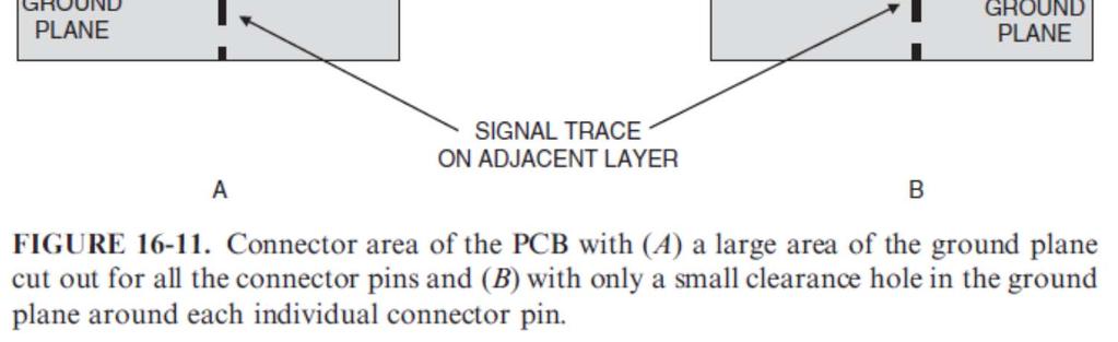
25 Return Path Discontinuities Connectors 25
26 Return Path Discontinuities Ground Fill Ground fill, or ground pour, is a technique where copper is introduced into areas of the PCB signal layers that contain no traces. The intent is to reduce emissions and susceptibility by reducing field fringing from the signal traces and by providing some degree of shielding on the board. To be effective, the fill must be connected to the existing ground structure on the board at many places. If not properly grounded, the copper fill can actually increase emissions and susceptibility, as well as crosstalk between traces. Copper fill, not properly grounded, can also create an ESD problem. Although often used with analog circuits on double-sided boards, copper fill is not recommended for high-speed digital circuits, because it can cause impedance discontinuities, which can lead to possible functional problems. 26
27 Return Path Discontinuities Ground Fill On multilayer boards, the ground fill, if used, must be connected to the PCB ground plane at multiple points. If ground fill is used on multilayer boards, it should only be applied to the surface layers. 27
The number of layers The number and types of planes (power and/or ground) The ordering or sequence of the layers The spacing between the layers
 The ordering or sequence of the layers The spacing between the layers") PCB Layer Stackup PCB layer stackup (the ordering of the layers and the layer spacing) is an important factor in determining the EMC performance of a product. The following four factors are important with
PCB Layer Stackup PCB layer stackup (the ordering of the layers and the layer spacing) is an important factor in determining the EMC performance of a product. The following four factors are important with
Split Planes in Multilayer PCBs
 by Barry Olney coulmn BEYOND DESIGN Split Planes in Multilayer PCBs Creating split planes or isolated islands in the copper planes of multilayer PCBs at first seems like a good idea. Today s high-speed
Chapter 12 Digital Circuit Radiation. Electromagnetic Compatibility Engineering. by Henry W. Ott
 Chapter 12 Digital Circuit Radiation Electromagnetic Compatibility Engineering by Henry W. Ott Forward Emission control should be treated as a design problem from the start, it should receive the necessary
Freescale Semiconductor, I
 Order this document by /D Noise Reduction Techniques for Microcontroller-Based Systems By Imad Kobeissi Introduction With today s advancements in semiconductor technology and the push toward faster microcontroller
Design for EMI & ESD compliance DESIGN FOR EMI & ESD COMPLIANCE
 DESIGN FOR EMI & ESD COMPLIANCE All of we know the causes & impacts of EMI & ESD on our boards & also on our final product. In this article, we will discuss some useful design procedures that can be followed
Top Ten EMC Problems
 Top Ten EMC Problems presented by: Kenneth Wyatt Sr. EMC Consultant EMC & RF Design, Troubleshooting, Consulting & Training 10 Northern Boulevard, Suite 1 Amherst, New Hampshire 03031 +1 603 578 1842 www.silent-solutions.com
EMI. Chris Herrick. Applications Engineer
 Fundamentals of EMI Chris Herrick Ansoft Applications Engineer Three Basic Elements of EMC Conduction Coupling process EMI source Emission Space & Field Conductive Capacitive Inductive Radiative Low, Middle
Class-D Audio Power Amplifiers: PCB Layout For Audio Quality, EMC & Thermal Success (Home Entertainment Devices)
") Class-D Audio Power Amplifiers: PCB Layout For Audio Quality, EMC & Thermal Success (Home Entertainment Devices) Stephen Crump http://e2e.ti.com Audio Power Amplifier Applications Audio and Imaging Products
Class-D Audio Power Amplifiers: PCB Layout For Audio Quality, EMC & Thermal Success (Home Entertainment Devices) Stephen Crump http://e2e.ti.com Audio Power Amplifier Applications Audio and Imaging Products
HT32 Series Crystal Oscillator, ADC Design Note and PCB Layout Guide
 HT32 Series rystal Oscillator, AD Design Note and PB Layout Guide HT32 Series rystal Oscillator, AD Design Note and PB Layout Guide D/N:AN0301E Introduction This application note provides some hardware
PCB Design Guidelines for Reduced EMI
 PCB Design Guidelines for Reduced EMI Guided By: Prof. Ruchi Gajjar Prepared By: Shukla Jay (13MECE17) Outline Power Distribution for Two-Layer Boards Gridding Power Traces on Two-Layer Boards Ferrite
PCB Design Guidelines for GPS chipset designs. Section 1. Section 2. Section 3. Section 4. Section 5
 PCB Design Guidelines for GPS chipset designs The main sections of this white paper are laid out follows: Section 1 Introduction Section 2 RF Design Issues Section 3 Sirf Receiver layout guidelines Section
11 Myths of EMI/EMC ORBEL.COM. Exploring common misconceptions and clarifying them. MYTH #1: EMI/EMC is black magic.
 11 Myths of EMI/EMC Exploring common misconceptions and clarifying them By Ed Nakauchi, Technical Consultant, Orbel Corporation What is a myth? A myth is defined as a popular belief or tradition that has
EL7302. Hardware Design Guide
 Hardware Design Guide Version: Preliminary 0.0 Date: January. 2005 Approval: Etron technology, Inc P.O. Box 19-54 No.6 Technology Road V. Science-based Industrial Park, Hsinchu,30077 Taiwan, R.O.C. Tel:
DEPARTMENT FOR CONTINUING EDUCATION
 DEPARTMENT FOR CONTINUING EDUCATION Reduce EMI Emissions for FREE! by Bruce Archambeault, Ph.D. (reprinted with permission from Bruce Archambeault) Bruce Archambeault presents two courses during the University
MINIMIZING EMI EFFECTS DURING PCB LAYOUT OF Z8/Z8PLUS CIRCUITS
 APPLICATION NOTE MINIMIZING EMI EFFECTS DURING PCB LAYOUT OF Z8/Z8PLUS CIRCUITS INTRODUCTION The Z8/Z8Plus families have redefined ease-of-use by being the simplest 8-bit microcontrollers to program. Combined
Technical Report Printed Circuit Board Decoupling Capacitor Performance For Optimum EMC Design
 Technical Report Printed Circuit Board Decoupling Capacitor Performance For Optimum EMC Design Bruce Archambeault, Ph.D. Doug White Personal Systems Group Electromagnetic Compatibility Center of Competency
Relationship Between Signal Integrity and EMC
 Relationship Between Signal Integrity and EMC Presented by Hasnain Syed Solectron USA, Inc. RTP, North Carolina Email: HasnainSyed@solectron.com 06/05/2007 Hasnain Syed 1 What is Signal Integrity (SI)?
Intel 82566/82562V Layout Checklist (version 1.0)
") Intel 82566/82562V Layout Checklist (version 1.0) Project Name Fab Revision Date Designer Intel Contact SECTION CHECK ITEMS REMARKS DONE General Ethernet Controller Obtain the most recent product documentation
Intel 82566/82562V Layout Checklist (version 1.0) Project Name Fab Revision Date Designer Intel Contact SECTION CHECK ITEMS REMARKS DONE General Ethernet Controller Obtain the most recent product documentation
Differential-Mode Emissions
 Differential-Mode Emissions In Fig. 13-5, the primary purpose of the capacitor C F, however, is to filter the full-wave rectified ac line voltage. The filter capacitor is therefore a large-value, high-voltage
Frequently Asked EMC Questions (and Answers)
") Frequently Asked EMC Questions (and Answers) Elya B. Joffe President Elect IEEE EMC Society e-mail: eb.joffe@ieee.org December 2, 2006 1 I think I know what the problem is 2 Top 10 EMC Questions 10, 9
Frequently Asked EMC Questions (and Answers) Elya B. Joffe President Elect IEEE EMC Society e-mail: eb.joffe@ieee.org December 2, 2006 1 I think I know what the problem is 2 Top 10 EMC Questions 10, 9
Common myths, fallacies and misconceptions in Electromagnetic Compatibility and their correction.
 Common myths, fallacies and misconceptions in Electromagnetic Compatibility and their correction. D. A. Weston EMC Consulting Inc 22-3-2010 These are some of the commonly held beliefs about EMC which are
LM2462 Monolithic Triple 3 ns CRT Driver
 LM2462 Monolithic Triple 3 ns CRT Driver General Description The LM2462 is an integrated high voltage CRT driver circuit designed for use in color monitor applications. The IC contains three high input
Understanding the Unintended Antenna Behavior of a Product
 Understanding the Unintended Antenna Behavior of a Product Colin E. Brench Southwest Research Institute Electromagnetic Compatibility Research and Testing colin.brench@swri.org Radiating System Source
EMC Design Guidelines C4ISR EQUIPMENT & SYSTEMS
 EMC Design Guidelines C4ISR EQUIPMENT & SYSTEMS 1.1. SHIELDING Enclosed structure (equipment box or chassis in outside RF environment) should provide at least 100 db of RF shielding at 1 MHz, 40 db at
The water-bed and the leaky bucket
 The water-bed and the leaky bucket Tim Williams Elmac Services Wareham, UK timw@elmac.co.uk Abstract The common situation of EMC mitigation measures having the opposite effect from what was intended, is
PI3DPX1207B Layout Guideline. Table of Contents. 1 Layout Design Guideline Power and GROUND High-speed Signal Routing...
 PI3DPX1207B Layout Guideline Table of Contents 1 Layout Design Guideline... 2 1.1 Power and GROUND... 2 1.2 High-speed Signal Routing... 3 2 PI3DPX1207B EVB layout... 8 3 Related Reference... 8 Page 1
EMC Design Guideline
 Partitioning separates the system into critical and non-critical sections from EMC point of view. Long I/O and power cables usually act as good antennas, picking up noise from the outside world and conducting
The Ground Myth IEEE. Bruce Archambeault, Ph.D. IBM Distinguished Engineer, IEEE Fellow 18 November 2008
 The Ground Myth Bruce Archambeault, Ph.D. IBM Distinguished Engineer, IEEE Fellow barch@us.ibm.com 18 November 2008 IEEE Introduction Electromagnetics can be scary Universities LOVE messy math EM is not
Texas Instruments DisplayPort Design Guide
 Texas Instruments DisplayPort Design Guide April 2009 1 High Speed Interface Applications Introduction This application note presents design guidelines, helping users of Texas Instruments DisplayPort devices
1. TABLE OF FIGURES APPLICATION NOTE OVERVIEW EMI...5
 APPLICATION NOTE 8.7 Rev 1.0 General Guidelines for Reduced Electromagnetic Interference utilizing the SMSC LAN83C175 EPIC 10/100 Mbps Ethernet Controller and Physical Layer Devices By Thomas Greene and
EMC for Printed Circuit Boards
 9 Bracken View, Brocton Stafford, Staffs, UK tel: +44 (0)1785 660 247 fax +44 (0)1785 660 247 email: keith.armstrong@cherryclough.com web: www.cherryclough.com EMC for Printed Circuit Boards Basic and
Electro-Magnetic Interference and Electro-Magnetic Compatibility (EMI/EMC)
") INTROUCTION Manufacturers of electrical and electronic equipment regularly submit their products for EMI/EMC testing to ensure regulations on electromagnetic compatibility are met. Inevitably, some equipment
INTROUCTION Manufacturers of electrical and electronic equipment regularly submit their products for EMI/EMC testing to ensure regulations on electromagnetic compatibility are met. Inevitably, some equipment
Introduction to Electromagnetic Compatibility
 Introduction to Electromagnetic Compatibility Second Edition CLAYTON R. PAUL Department of Electrical and Computer Engineering, School of Engineering, Mercer University, Macon, Georgia and Emeritus Professor
LM2412 Monolithic Triple 2.8 ns CRT Driver
 Monolithic Triple 2.8 ns CRT Driver General Description The is an integrated high voltage CRT driver circuit designed for use in high resolution color monitor applications. The IC contains three high input
White paper. High speed and RF PCB routing : Best practises and recommandations
 ALCIOM 5, Parvis Robert Schuman 92370 CHAVILLE - FRANCE Tel/Fax : 01 47 09 30 51 contact@alciom.com www.alciom.com Projet : White paper DOCUMENT : High speed and RF PCB routing : Best practises and recommandations
Course Introduction. Content: 19 pages 3 questions. Learning Time: 30 minutes
 Course Introduction Purpose: This course discusses techniques that can be applied to reduce problems in embedded control systems caused by electromagnetic noise Objectives: Gain a basic knowledge about
RF PCB Design. Presented by: Henry Lau, Lexiwave Technology, Inc. Sponsored by: National Instruments (formerly AWR Corp.) October 15, 2015.
 October 15, 2015.") RF PCB Design Presented by: Henry Lau, Lexiwave Technology, Inc. Sponsored by: National Instruments (formerly AWR Corp.) October 15, 2015 1 ni.com/awr NI AWR Software Product Line Overview ni.com/awr NI
RF PCB Design Presented by: Henry Lau, Lexiwave Technology, Inc. Sponsored by: National Instruments (formerly AWR Corp.) October 15, 2015 1 ni.com/awr NI AWR Software Product Line Overview ni.com/awr NI
MPC5606E: Design for Performance and Electromagnetic Compatibility
 Freescale Semiconductor, Inc. Document Number: AN5100 Application Note MPC5606E: Design for Performance and Electromagnetic Compatibility by: Tomas Kulig 1. Introduction This document provides information
Presented by Joanna Hill
 Santa Clara IEEE EMC Chapter meeting April 9, 2013 Dorothy we're not in Kansas any more, we are in Impedance land. Oh my! Presented by Joanna Hill Cell 248-765-3599 jhill28590@comcast.net Welcome to Impedance
HOW SMALL PCB DESIGN TEAMS CAN SOLVE HIGH-SPEED DESIGN CHALLENGES WITH DESIGN RULE CHECKING MENTOR GRAPHICS
 HOW SMALL PCB DESIGN TEAMS CAN SOLVE HIGH-SPEED DESIGN CHALLENGES WITH DESIGN RULE CHECKING MENTOR GRAPHICS H I G H S P E E D D E S I G N W H I T E P A P E R w w w. p a d s. c o m INTRODUCTION Coping with
PHY Layout APPLICATION REPORT: SLLA020. Ron Raybarman Burke S. Henehan 1394 Applications Group
 PHY Layout APPLICATION REPORT: SLLA020 Ron Raybarman Burke S. Henehan 1394 Applications Group Mixed Signal and Logic Products Bus Solutions November 1997 IMPORTANT NOTICE Texas Instruments (TI) reserves
BASIS OF ELECTROMAGNETIC COMPATIBILITY OF INTEGRATED CIRCUIT Chapter VI - MODELLING PCB INTERCONNECTS Corrections of exercises
 BASIS OF ELECTROMAGNETIC COMPATIBILITY OF INTEGRATED CIRCUIT Chapter VI - MODELLING PCB INTERCONNECTS Corrections of exercises I. EXERCISE NO 1 - Spot the PCB design errors Spot the six design errors in
Low Jitter, Low Emission Timing Solutions For High Speed Digital Systems. A Design Methodology
 Low Jitter, Low Emission Timing Solutions For High Speed Digital Systems A Design Methodology The Challenges of High Speed Digital Clock Design In high speed applications, the faster the signal moves through
Facility Grounding & Bonding Based on the EMC/PI/SI Model for a High Speed PCB/Cabinet
 Facility Grounding & Bonding Based on the EMC/PI/SI Model for a High Speed PCB/Cabinet and: SILICON LABS AN203 PRINTED CIRCUIT BOARD DESIGN NOTES www.silabs.com William Bush (wbush@ieee.org) Industry Consultant
Predicting and Controlling Common Mode Noise from High Speed Differential Signals
 Predicting and Controlling Common Mode Noise from High Speed Differential Signals Bruce Archambeault, Ph.D. IEEE Fellow, inarte Certified Master EMC Design Engineer, Missouri University of Science & Technology
CMT2300AW Schematic and PCB Layout Design Guideline
 AN141 CMT2300AW Schematic and PCB Layout Design Guideline Introduction This document is the CMT2300AW Application Development Guideline. It will explain how to design and use the CMT2300AW schematic and
AN4819 Application note
 Application note PCB design guidelines for the BlueNRG-1 device Introduction The BlueNRG1 is a very low power Bluetooth low energy (BLE) single-mode system-on-chip compliant with Bluetooth specification
LM V Monolithic Triple Channel 15 MHz CRT DTV Driver
 220V Monolithic Triple Channel 15 MHz CRT DTV Driver General Description The is a triple channel high voltage CRT driver circuit designed for use in DTV applications. The IC contains three high input impedance,
2. Design Recommendations when Using EZRadioPRO RF ICs
 EZRADIOPRO LAYOUT DESIGN GUIDE 1. Introduction The purpose of this application note is to help users design EZRadioPRO PCBs using design practices that allow for good RF performance. This application note
Top Ten EMC Problems & EMC Troubleshooting Techniques by Kenneth Wyatt, DVD, Colorado Springs Rev. 1, Feb 26, 2007
 EMC Engineering Top Ten EMC Problems & EMC Troubleshooting Techniques by Kenneth Wyatt, DVD, Colorado Springs Rev. 1, Feb 26, 2007 1a. Ground Impedance The overwhelming majority of high-frequency problems,
Advanced Topics in EMC Design. Issue 1: The ground plane to split or not to split?
 NEEDS 2006 workshop Advanced Topics in EMC Design Tim Williams Elmac Services C o n s u l t a n c y a n d t r a i n i n g i n e l e c t r o m a g n e t i c c o m p a t i b i l i t y e-mail timw@elmac.co.uk
Electromagnetic Compatibility Engineering. Henry W. Ott Henry Ott Consultants
 Electromagnetic Compatibility Engineering Henry W. Ott Henry Ott Consultants Electromagnetic Compatibility Engineering Electromagnetic Compatibility Engineering Henry W. Ott Henry Ott Consultants Copyright
Electromagnetic Compatibility Engineering
 Electromagnetic Compatibility Engineering Electromagnetic Compatibility Engineering Henry W. Ott Henry Ott Consultants Copyright r 2009 by John Wiley & Sons, Inc. All rights reserved. Published by John
Verifying Simulation Results with Measurements. Scott Piper General Motors
 Verifying Simulation Results with Measurements Scott Piper General Motors EM Simulation Software Can be easy to justify the purchase of software packages even costing tens of thousands of dollars Upper
AN1705. Motorola Semiconductor Application Note. Noise Reduction Techniques for Microcontroller-Based Systems. Introduction
 Order this document by /D Motorola Semiconductor Application Note Noise Reduction Techniques for Microcontroller-Based Systems By Imad Kobeissi Introduction With today s advancements in semiconductor technology
Testing for EMC Compliance: Approaches and Techniques October 12, 2006
 : Approaches and Techniques October 12, 2006 Ed Nakauchi EMI/EMC/ESD/EMP Consultant Emulex Corporation 1 Outline Discuss EMC Basics & Physics Fault Isolation Techniques Tools & Techniques Correlation Analyzer
CMOS is Different: PCB Design for Both Low Noise and Low EMI
 CMOS is Different: PCB Design for Both Low Noise and Low EMI Author : Earl McCune 09/17/2013 Earl McCune, RF Communications Consulting ABSTRACT Achieving low power supply noise does not automatically assure
Common myths, fallacies and misconceptions in Electromagnetic Compatibility and their correction.
 Common myths, fallacies and misconceptions in Electromagnetic Compatibility and their correction. D. A. Weston EMC Consulting Inc 15-3-2013 1) First topic an introduction These are some of the commonly
HV739 ±100V 3.0A Ultrasound Pulser Demo Board
 HV79 ±00V.0A Ultrasound Pulser Demo Board HV79DB Introduction The HV79 is a monolithic single channel, high-speed, high voltage, ultrasound transmitter pulser. This integrated, high performance circuit
Antenna Matching Within an Enclosure Part II: Practical Techniques and Guidelines
 Antenna Matching Within an Enclosure Part II: Practical Techniques and Guidelines By Johnny Lienau, RF Engineer June 2012 Antenna selection and placement can be a difficult task, and the challenges of
PCI-EXPRESS CLOCK SOURCE. Features
 DATASHEET ICS557-01 Description The ICS557-01 is a clock chip designed for use in PCI-Express Cards as a clock source. It provides a pair of differential outputs at 100 MHz in a small 8-pin SOIC package.
Designing for Electromagnetic Interference (EMI) Compliance
 Compliance") Designing for Electromagnetic Interference (EMI) Compliance Application Note by Tim Raper and Steve Knauber This application note describes how to integrate any microprocessor or microcontroller into an
Designing for Electromagnetic Interference (EMI) Compliance Application Note by Tim Raper and Steve Knauber This application note describes how to integrate any microprocessor or microcontroller into an
Henry Lau Lexiwave Technology, Inc
 RF PCB Design Henry Lau Lexiwave Technology, Inc December 4, 2012 1 AWR Corporation Overview & Introduction AWR - At a Glance The Innovation Leader in High-Frequency EDA Product Portfolio: Microwave Office
LM2405 Monolithic Triple 7 ns CRT Driver
 LM2405 Monolithic Triple 7 ns CRT Driver General Description The LM2405 is an integrated high voltage CRT driver circuit designed for use in color monitor applications The IC contains three high input
Plane Crazy, Part 2 BEYOND DESIGN. by Barry Olney
 by Barry Olney column BEYOND DESIGN Plane Crazy, Part 2 In my recent four-part series on stackup planning, I described the best configurations for various stackup requirements. But I did not have the opportunity
EMI AND BEL MAGNETIC ICM
 EMI AND BEL MAGNETIC ICM ABSTRACT Electromagnetic interference (EMI) in a local area network (LAN) system is a common problem that every LAN system designer faces, and it is a growing problem because the
TN ADC design guidelines. Document information
 Rev. 1 8 May 2014 Technical note Document information Info Content Keywords Abstract This technical note provides common best practices for board layout required when Analog circuits (which are sensitive
Solutions for EMC Issues in Automotive System Transmission Lines
 Solutions for EMC Issues in Automotive System Transmission Lines Todd H. Hubing Michelin Professor of Vehicle Electronics Clemson University A P R. 1 0. 2 0 1 4 TM External Use EMC Requirements and Key
Decoupling capacitor placement
 Decoupling capacitor placement Covered in this topic: Introduction Which locations need decoupling caps? IC decoupling Capacitor lumped model How to maximize the effectiveness of a decoupling cap Parallel
ICS LOW EMI CLOCK GENERATOR. Description. Features. Block Diagram DATASHEET
 DATASHEET ICS180-51 Description The ICS180-51 generates a low EMI output clock from a clock or crystal input. The device uses IDT s proprietary mix of analog and digital Phase-Locked Loop (PLL) technology
Solutions for EMC Issues in Automotive System Transmission Lines
 June 23, 2010 Solutions for EMC Issues in Automotive System Transmission Lines FTF-ENT-F0174 Todd Hubing Clemson University and VortiQa are trademarks of Freescale Semiconductor, Inc. All other product
Categorized by the type of core on which inductors are wound:
 Inductors Categorized by the type of core on which inductors are wound: air core and magnetic core. The magnetic core inductors can be subdivided depending on whether the core is open or closed. Equivalent
ICS PCI-EXPRESS CLOCK SOURCE. Description. Features. Block Diagram DATASHEET
 DATASHEET ICS557-0 Description The ICS557-0 is a clock chip designed for use in PCI-Express Cards as a clock source. It provides a pair of differential outputs at 00 MHz in a small 8-pin SOIC package.
The Impact Of Signal Jumping Across Multiple Different Reference Planes On Electromagnetic Compatibility
 Copyright by Dr. Andrew David Norte, All Rights Reserved March 18 th, 2012 The Impact Of Signal Jumping Across Multiple Different Reference Planes On Electromagnetic Compatibility David Norte, PhD www.the-signal-and-power-integrity-institute.com
Exclusive Technology Feature. Integrated Driver Shrinks Class D Audio Amplifiers. Audio Driver Features. ISSUE: November 2009
 ISSUE: November 2009 Integrated Driver Shrinks Class D Audio Amplifiers By Jun Honda, International Rectifier, El Segundo, Calif. From automotive entertainment to home theater systems, consumers are demanding
Reducing Motor Drive Radiated Emissions
 Volume 2, Number 2, April, 1996 Application Note 107 Donald E. Fulton Reducing Motor Drive Radiated Emissions Introduction This application note discusses radiated emissions (30 Mhz+) of motor drives and
Designing for Board Level Electromagnetic Compatibility
 Freescale Semiconductor Application Note AN2321 Rev. 1, 10/2005 Designing for Board Level Electromagnetic Compatibility by: T.C. Lun Applications Engineering Microcontroller Division This application note
PCB layout guidelines for MOSFET gate driver
 AN_1801_PL52_1801_132230 PCB layout guidelines for MOSFET gate driver About this document Scope and purpose The PCB layout is essential to the optimal function of the MOSFET gate driver. It is also essential
AN383. Si47XX ANTENNA, SCHEMATIC, LAYOUT, AND DESIGN GUIDELINES. 1. Introduction
 Si47XX ANTENNA, SCHEMATIC, LAYOUT, AND DESIGN GUIDELINES 1. Introduction This document provides general Si47xx design guidelines and AM/FM/SW/LW/WB antenna selections which includes schematic, BOM, layout
Microcircuit Electrical Issues
 Microcircuit Electrical Issues Distortion The frequency at which transmitted power has dropped to 50 percent of the injected power is called the "3 db" point and is used to define the bandwidth of the
International Journal of Innovative Research in Science, Engineering and Technology. (An ISO 3297: 2007 Certified Organization)
") Optimized Routing and Component Placement to Improve the Continuity And Uniformity of the PCB- PIFL Antenna s Co-Planar Ground Plane to Achieve an Overall Improved Antenna Performance SegeraDavies 1, MwangiMbuthia
Optimized Routing and Component Placement to Improve the Continuity And Uniformity of the PCB- PIFL Antenna s Co-Planar Ground Plane to Achieve an Overall Improved Antenna Performance SegeraDavies 1, MwangiMbuthia
PHY DESIGN RECOMMENDATIONS FOR PCB LAYOUT
 PHY DESIGN RECOMMENDATIONS FOR PCB LAYOUT Ron Raybarman s-raybarman1@ti ti.com Texas Instruments Topics of discussion: 1. Specific for 1394 - (Not generic PCB layout) Etch lengths Termination Network Skew
Signal Integrity, Part 1 of 3
 by Barry Olney feature column BEYOND DESIGN Signal Integrity, Part 1 of 3 As system performance increases, the PCB designer s challenges become more complex. The impact of lower core voltages, high frequencies
High-Speed PCB Design und EMV Minimierung
 TRAINING Bei dem hier beschriebenen Training handelt es sich um ein Cadence Standard Training. Sie erhalten eine Dokumentation in englischer Sprache. Die Trainingssprache ist deutsch, falls nicht anders
Harmonizing the ANSI-C12.1(2008) EMC Tests. Harmonizing the ANSI-C12.1(2008) EMC Tests
 EMC Tests. Harmonizing the ANSI-C12.1(2008) EMC Tests") Harmonizing the ANSI-C12.1(2008) EMC Tests Subcommittee 1 (Emissions) Subcommittee 5 (Immunity) Joint Task Force on C12.1 June 17, 2013 1 The Accredited Standards Committee C63 presents Harmonizing the
Harmonizing the ANSI-C12.1(2008) EMC Tests Subcommittee 1 (Emissions) Subcommittee 5 (Immunity) Joint Task Force on C12.1 June 17, 2013 1 The Accredited Standards Committee C63 presents Harmonizing the
Impedance Matching to 50Ω
 Impedance Matching to 50Ω The figure above shows the output matching circuit as implemented on the TRF7960EVM on a simulated Smith chart plot going from the nominal 4 Ohm TX_OUT (Pin 5) to near 50 Ohms
SMT Module RF Reference Design Guide. AN_ SMT Module RF Reference Design Guide _V1.01
 SMT Module RF Reference Design Guide AN_ SMT Module RF Reference Design Guide _V1.01 Document Title: SMT Module RF Reference Design Guide Version: 1.01 Date: 2010-2-10 Status: Document Control ID: Release
10 Safety earthing/grounding does not help EMC at RF
 1of 6 series Webinar #3 of 3, August 28, 2013 Grounding, Immunity, Overviews of Emissions and Immunity, and Crosstalk Contents of Webinar #3 Topics 1 through 9 were covered by the previous two webinars
Introduction to Board Level Simulation and the PCB Design Process
 BEYOND DESIGN C O L U M N Introduction to Board Level Simulation and the PCB Design Process by Barry Olney IN-CIRCUIT DESIGN PTY LTD AUSTRALIA SUMMARY Board-level simulation reduces costs by identifying
Peak Reducing EMI Solution
 Peak Reducing EMI Solution Features Cypress PREMIS family offering enerates an EMI optimized clocking signal at the output Selectable input to output frequency Single 1.% or.% down or center spread output
BIRD 74 - recap. April 7, Minor revisions Jan. 22, 2009
 BIRD 74 - recap April 7, 2003 Minor revisions Jan. 22, 2009 Please direct comments, questions to the author listed below: Guy de Burgh, EM Integrity mail to: gdeburgh@nc.rr.com (919) 457-6050 Copyright
Common Impedance Coupling Effect on Video and Audio Circuitry. Prof. Bogdan Adamczyk Grand Valley State University
 Common Impedance Coupling Effect on Video and Audio Circuitry Prof. Bogdan Adamczyk rand Valley State University Outline 1. Signal ground (signal return path) 2. Objectives of grounding 3. Single- vs.
ENT-AN0098 Application Note. Magnetics Guide. June 2018
 ENT-AN0098 Application Note Magnetics Guide June 2018 Contents 1 Revision History... 1 1.1 Revision 2.2... 1 1.2 Revision 2.1... 1 1.3 Revision 2.0... 1 1.4 Revision 1.2... 1 1.5 Revision 1.1... 1 1.6
7. EMV Fachtagung. EMV-gerechtes Filterdesign. 23. April 2009, TU-Graz. Dr. Gunter Winkler (TU Graz) Dr. Bernd Deutschmann (Infineon Technologies AG)
 Dr. Bernd Deutschmann (Infineon Technologies AG)") 7. EMV Fachtagung 23. April 2009, TU-Graz EMV-gerechtes Filterdesign Dr. Gunter Winkler (TU Graz) Dr. Bernd Deutschmann (Infineon Technologies AG) Page 1 Agenda Filter design basics Filter Attenuation
7. EMV Fachtagung 23. April 2009, TU-Graz EMV-gerechtes Filterdesign Dr. Gunter Winkler (TU Graz) Dr. Bernd Deutschmann (Infineon Technologies AG) Page 1 Agenda Filter design basics Filter Attenuation
Understanding and Optimizing Electromagnetic Compatibility in Switchmode Power Supplies
 Understanding and Optimizing Electromagnetic Compatibility in Switchmode Power Supplies 1 Definitions EMI = Electro Magnetic Interference EMC = Electro Magnetic Compatibility (No EMI) Three Components
EMI Filters Demystified. By William R. Bill Limburg February 21, 2018 Phoenix Chapter, IEEE EMC Society
 EMI Filters Demystified By William R. Bill Limburg February 21, 2018 Phoenix Chapter, IEEE EMC Society An EMI Filter Defined An EMI filter is a network designed to prevent unwanted electrical conducted
Modeling of Power Planes for Improving EMC in High Speed Medical System
 Modeling of Power Planes for Improving EMC in High Speed Medical System Surender Singh, Dr. Ravinder Agarwal* *Prof : Dept of Instrumentation Engineering Thapar University, Patiala, India Dr. V. R. Singh
SGM9154 Single Channel, Video Filter Driver for HD (1080p)
") PRODUCT DESCRIPTION The SGM9154 video filter is intended to replace passive LC filters and drivers with an integrated device. The 6th-order channel offers High Definition (HDp) filter. The SGM9154 may
PRODUCT DESCRIPTION The SGM9154 video filter is intended to replace passive LC filters and drivers with an integrated device. The 6th-order channel offers High Definition (HDp) filter. The SGM9154 may
Recommendations for PHY Layout
 Recommendations for PHY Layout Ron Raybarman 1394 Applications Group Abstract This document makes recommendations for the layout of the PHY and Link layer devices in an IEEE 1394 environment. The optimal
High Speed Clock Distribution Design Techniques for CDC 509/516/2509/2510/2516
 High Speed Clock Distribution Design Techniques for CDC 509/516/2509/2510/2516 APPLICATION REPORT: SLMA003A Boyd Barrie Bus Solutions Mixed Signals DSP Solutions September 1998 IMPORTANT NOTICE Texas Instruments