Technical Report Printed Circuit Board Decoupling Capacitor Performance For Optimum EMC Design
|
|
|
- Collin Snow
- 5 years ago
- Views:
Transcription
1 Technical Report Printed Circuit Board Decoupling Capacitor Performance For Optimum EMC Design Bruce Archambeault, Ph.D. Doug White Personal Systems Group Electromagnetic Compatibility Center of Competency January
2 Abstract The optimum design of decoupling capacitors on a printed circuit (PC) board has been the subject of debate and opinion for many years. Cause and effect have been difficult to separate from all the other effects occuring on a normal active PC board. This work used a specially designed PC board to allow the measruement and characterization of the effects of various decoupling capacitor strageties. Many common opinions and myths are investigated, and the optimum design stragety recommended based upon the measured data in this report. ITIRC Keywords: Decoupling EMI/EMC Power Plane 2
3 Table of Contents Introduction. 4 Decoupling Capacitor Performance Measurement Process. 4 Test Board Description. 4 Decoupling Capacitor Configuration Measurement Results. 6 PC Board Impedance 7 Source vs. Distributed Decoupling. 7 Quanity of Distributed Decoupling Capacitors (.01 uf only) 12 Quanity of Distributed Decoupling Capacitors (.01 uf and 10 pf) 12 Quanity of Distributed Decoupling Capacitors (.01 uf and 22 pf) 13 Quanity of Distributed Decoupling Capacitors (.01 uf and 330 pf).. 32 Decoupling Around Board Edge Only 32 Resistive Decoupling Around Board Edge. 32 Emissions Around Board Edge. 32 Conclusions and Recommendations 32 3
4 Technical Report Printed Circuit Board Decoupling Capacitor Performance For Optimum EMC Design Bruce Archambeault, Ph.D. Doug White Personal Systems Group Electromagnetic Compatibility Center of Competency January 1999 INTRODUCTION Decoupling capacitors are used to provide a local source of charge for ICs requiring a significant amount of supply current in response to internal switching. If sufficient decoupling capacitors are not used, the required supply current is not available, and the device does not operate properly, and signal integrity data errors can result. In addition to the signal integrity requirement, decoupling capacitors serve as EMC filters to prevent high frequency RF signals from propagating throughout the PC board. This requires them to provide a low impedance across the frequencies of interest. The proper number of decoupling capacitors, and the proper value of those decoupling capacitors is always a topic of debate between EMC engineers and design engineers. Some typical rules-ofthumb require a decoupling capacitor for each power pin on an IC. Other rules-of-thumb require at least one decoupling capacitor per side of physically large ICs. Still other rules-of-thumb require decoupling capacitors spread evenly over every square inch of the board. Very little real information about the optimum approach is available in the technical literature. Traditionally, the values of the decoupling capacitors are largely based upon habit and the experience of the EMC engineer. Values of.10 uf are typically used. Often smaller capacitors are used in parallel with the main decoupling capacitor to provide a high frequency and a low frequency filtering effect. However, potential cross resonances can have a negative effect when using multiple capacitors in close proximity. The overall result is that the design of the power plane decoupling (between a power plane and a ground reference plane) has been historically difficult to properly design or analyze. With onboard clock speeds of MHz becoming common, a more rational approach must be taken to optimize the design of decoupling capacitors on the printed circuit (PC) board. DECOUPLING CAPACITOR PERFORMANCE MEASUREMENT PROCESS Since a real PC board is quite complex, it is difficult to isolate the various EMC effects to know that a particular change to the board has produced an effect that is directly traceable to that original change. Therefore, a special PC board was created to help analyze the effects of a variety of decoupling capacitor configurations. Test Board Description This investigation focused upon a 4-layer PC board, with the external dimensions of 10 x 12 inches. This was considered to be a typical board used in current products. Since the frequency range under investigation extended from 30 MHz to over 1 GHz, a repeatable and well controlled connection method to the test board was required. A set of 15 SMA connectors were installed across the board as shown in Figure 1. Each of the SMA connectors was surrounded by four locations for SMT decoupling capacitors. Figure 2 shows the detail of each location. 4
5 Figure 1 Test Board SMA Connector Configuration Decoupling Caps SMA Connector Area Figure 2 Test Board SMA Connector Area Detail 5
6 In addition to the SMA connectors, and the surrounding decoupling capacitor sites, locations for additional SMT decouping capacitors were located every inch on the PC board. Figure 3 shows a Possible Cap Location Figure 3 Additional Decoupling Capacitor Locations on Test Board diagram of the additional decoupling capacitor locations. All measurements were taken with a Network/Impedance analyzer. Both one-port and two-port measurements were used. One port measurements were impedance measurements, while the two port measurements were S21 1. Examples of each result will be provided in the following section. Initial measurements were impedance measurements. Observing the impedance across the frequency range of MHz allowed a better understanding of the effectiveness of the natural interplane capacitance, the effects of decoupling capacitors, and board resonances. However, impedance at a given location on a PC board is not the primary concern for EMC engineers. A more important parameter for EMC engineers is the amount of noise 2 at a remote location due to some IC source location. The remote location might be the edge of the PC board (where it was located near a seam in the metal shielded enclosure), or near a via for an I/O signal trace, which was then connected to an external connector. Therefore, the S21 parameter is a better indication of the decoupling configuration s performance for EMC considerations. The goal is to have as low as possible S21 between a potential source, and a remote location of concern. Decoupling Capacitor Configuration Measurement Results There was a number of different types of configurations measured, as well as the capacitor value being varied. Initial measurements focused on impedance of the board at various locations, and with different configurations of capacitors. The difference between local source decoupling, and distributed decoupling was then investigated. Finally, the number of capacitors, and various values of capacitance (both single and multiple values) were investigated. 1 S21 is a measure of the voltage at a remote location due to a source voltage. 2 The noise in this case is due to the switching within the IC, and the current drawn from the power/ground plane structure to support the sudden switching. 6
7 PC Board Impedance The impedance of the PC board with no capacitors was measured using the impedance analyzer, at various locations across the board. The results are shown in Figure 4. The natural inter-plane capacitance is dominant at low frequencies (below 70 MHz), as shown by the impedance decreasing as frequency increases. The measured impedance values match very closely the impedance calculated using a simple parallel plate capacitor formula at low frequencies. At about 70 MHz, the self resonance of the board capacitance and inductance has become dominant, and the impedance begins to rise (inductive component) with frequency. Above 200 MHz, resonances due to the board dimensions become the dominant factor. Depending upon which location on the PC board was used for the impedance measurement, a particular resonant frequency might be excited, or might not be excited. However, from an EMC point of view, it is not possible to control where a component might be placed so to ensure a particular resonance mode would not be excited, so all modes must be assumed present. For this set of experiments, the corner port was used so that most of the resonant modes would be excited over the frequency range of interest (< 2 GHz). Further experiments with various capacitor values at various locations showed that while a particular resonant frequency would shift to another frequency (as capacitors were added and/or moved about the board), the general shape and level of impedance of the resonant peaks did not change. This indicates that the entire resonant frequency range must be considered resonant. That is, since the frequency of resonance shift with any changes, then all frequencies must be assumed to be resonant, and the overall envelop of the impedance (or S21) lowered. Source vs Distributed Decoupling As mentioned earlier, a common question amongst EMC and design engineers is whether to place decoupling capacitors close to the source of the noise (that is, near the power and/or ground pins of the ICs), or to simply distribute them across the entire board. To help determine the proposed design approach, the impedance and the S21 of the test PC board were measured with no capacitors, and then with capacitors only around the source SMA connector, and then with capacitors distributed across the entire board. As a further test, the source-only configuration was tested with one, two, three, and four capacitors placed around the SMA connector. Figure 5 shows the impedance results for no capacitors and source-only capacitors. The capacitors did not tend to significantly lower the overall impedance envelop, in fact, some configurations increased the impedance at certain resonant frequencies. Further testing was performed to compare the effects of having.01uf capacitors distributed across the entire board, and only at the source location. Figure 6 shows the S21 results between ports 8 and 10 on the test PC board. (Note that the scales have been changed to better display the S21 data, and that a log (db) scale is now used for S21 amplitude.) 3 The results in Figure 6 show that very little improvement 4 was observed at frequencies above 200 MHz. However, the impedance of the.01uf capacitor SMT capacitor is greatly affected by it s internal inductance (and the inductance of the pads and vias on the board). Figure 7 shows a typical SMT.01uf 3 If S21 is equal to one, or zero db, that would indicate that all the source voltage was present at the remote observation point. 4 From an EMC point of view, a lower S21 result is a better result. 7
8 Figure 4 8
9 Figure 5 9
10 Figure 6 10
11 Figure 7 11
12 capacitor s impedance. Note that the self resonant frequency is about 60 MHz. Also note that the capacitor s impedance is quite high above 200 MHz, which explains why there is so little effect on the test PC board above 200 MHz. However, in the frequency range where the capacitor is a low impedance, the S21 results in Figure 6 show a definite improvement with the distributed capacitance configuration. The S21 parameter is significantly lower in the below 200 MHz frequency range. This indicates a definite improvement using the distributed capacitance configuration. While a distributed decoupling strategy appears to be best for an EMC design, signal integrity design considerations still require a decoupling capacitor near a high speed IC to provide the necessary supply current with as low series inductance as possible. A combination of decoupling strategies will meet both EMC and signal integrity requirements. Quantity of Distributed Decoupling Capacitors (.01uf Only) The investigation into the number of decoupling capacitors distributed across the board used only.01uf SMT capacitors. The S21 transfer function was measured for a variety of different port combinations, and with a variety of capacitors distributed across the board. Every effort was made to distribute the capacitors evenly across the board for all quantities of capacitors. Table 1 shows the figure number for the various S21 transfer function ports. Table 1 S21 Port to Figure Definitions (.01uf Caps Only) S21 Ports Figure Number 1-to-8 Figure 8 2-to-8 Figure 9 3-to8 Figure 10 5-to-8 Figure 11 6-to-8 Figure 12 7-to-8 Figure 13 As can be seen in Figures 8 through 13, the more capacitors, the lower the S21 transfer function in the lower frequency ranges (below MHz). Also, at higher frequencies, the overall envelop for the S21 transfer function decreased slightly (even though the resonant frequency shifted) as more capacitors were added. The maximum number of capacitors was 99 distributed capacitors, representing one capacitor every square inch across the PC test board. Figure 14 shows a summary of all the various transfer function ports with the full (99) number of capacitors. Quantity of Distributed Decoupling Capacitors (.01uf and 10pf) Since the.01uf capacitors had a limited effective frequency range, a 10 pf capacitor was placed in parallel with the original.01uf capacitors to determine the improvement at high frequencies. For this set of experiments, the test PC board was populated with.01 uf and 10 pf capacitors. The 10 pf capacitors were placed in piggy-back fashion on top of the.01 uf capacitors. This resulted in a low-as-possible inductance between the two different values of capacitor. 5 This set of experiments was again repeated for a number of different port-to-port combinations, and with a number of different configurations with varying amounts of capacitor combinations. Table 2 shows the index of test result figures to port-to-port configurations. 5 It is understood that this piggy-back arrangement is not practical from a manufacturing point of view. However, it does serve to demonstrate the best possible performance due to the least possible inductance.
13 Table 2 S21 Port to Figure Definitions (.01uf and 10 pf Caps) S21 Ports Figure Number 1-to-8 Figure 15 2-to-8 Figure 16 3-to8 Figure 17 6-to-8 Figure 18 7-to-8 Figure 19 2-to-15 Figure 20 The results show that at low frequencies, the S21 behavior is very similar to the case with only.01 uf capacitors. However, in the frequency range of 1000 to 1200 MHz, the increasing number of 10 pf capacitors had a significant effect and lowered the S21 parameter as more capacitors were added. There seemed to be little improvement after 33 capacitors were added, indicating that all 99 positions were not necessary. Quantity of Distributed Decoupling Capacitors (.01uf and 22pf) The 10 pf capacitors were then replaced with 22 pf capacitors to determine the effect on the high frequency performance of S21. For this set of experiments, the test PC board was completely populated with.01 uf capacitors (all 99 locations had a.01 uf capacitor, regardless of the presence of a 22 pf capacitor or not). The 22 pf capacitors were again placed in piggy-back fashion on top of the.01 uf capacitors. This resulted in a low-as-possible inductance between the two different values of capacitor. 6 This set of experiments was again repeated for a number of different port-to-port combinations, and with a number of different configurations with varying amounts of capacitor combinations. Table 3 shows the index of test result figures to port-to-port configurations. Table 3 S21 Port to Figure Definitions (.01uf and 22 pf Caps) S21 Ports Figure Number 1-to-8 Figure 21 2-to-8 Figure 22 3-to8 Figure 23 6-to-8 Figure 24 7-to-8 Figure 25 The results show that at low frequencies, the S21 behavior is very similar to the case with only.01 uf capacitors. Some small effect was observed in the MHz frequency range, and at a lower frequency than the similar effect with 10 pf capacitors (as expected since the capacitance value increased), but the effect was not as significant as the 10 pf case. Note that the case with only.01 uf capacitors is plotted (again) on these figures as a reference in a heavy line-type. 6 It is understood that this piggy-back arrangement is not practical from a manufacturing point of view. However, it does serve to demonstrate the best possible performance due to the least possible inductance. 13
14 Figure 8 14
15 Figure 9 15
16 Figure 10 16
17 Figure 11 17
18 Figure 12 18
19 Figure 13 19
20 Figure 14 20
21 Figure 15 21
22 Figure 16 22
23 Figure 17 23
24 Figure 18 24
25 Figure 19 25
26 Figure 20 26
27 Figure 21 27
28 Figure 22 28
29 Figure 23 29
30 Figure 24 30
31 Figure 25 31
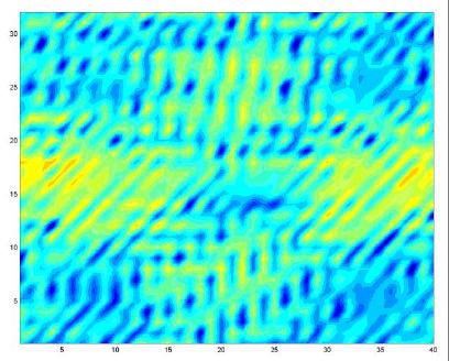
32 Quantity of Distributed Decoupling Capacitors (.01uf and 330pf) The 22 pf capacitors were then replaced with 330 pf capacitors to determine the effect on the high frequency performance of S21. For this set of experiments, the test PC board was completely populated with alternating.01 uf and 330 pf capacitors (all 99 locations had a.01 uf capacitor or a 330 pf capacitor, but not both values). This set of experiments was again repeated for a number of different port-to-port combinations. Figure 26 shows the test result of various port-to-port configurations. The results show that at low frequencies, the S21 behavior is very similar to the case with only.01 uf capacitors. However, the improved low frequency performance is increased to a higher frequency with the addition of the second value of capacitor (330 pf). Decoupling Around Board Edge Only A set of experiments were conducted with the decoupling capacitors only around the outer edge of the test board. Figure 27 shows the various S21 port-to-port measurements for the case with only.01 uf capacitors, and Figure 28 shows the results when 10 pf capacitors are added. Only the outer edge locations were populated with capacitors. There was no clear improvement with this configuration, and in fact, the fully populated board results were better, especially at low frequencies (below 400 MHz). Resistive Decoupling Around Board Edge A set of experiments were conducted with a resistor-capacitor combination placed around the outer edge of the test board. Figures 29 through 31 show the various port-to-port S21 measurement results for the case with only a 470 pf capacitor, a 470 pf capacitor and 20 ohm resistor, and a 470 pf capacitor and 2.2 ohm resistor. The plain.01uf capacitor case was also reploted on Figure 29 for reference. There was some improvement in the S21 at higher frequencies with the R-C decoupling combination. However, lower frequencies were significantly better with the fully distributed capacitor configuration. EMISSIONS AROUND THE EDGE OF THE BOARD It was determined that the primary emissions from the test board was around the edge of the board, rather than off the top or bottom plane. Figure 32a and 32b shows the field scan from EMSCAN for a particular frequency. Each color indicates a 10 db change in amplitude. A standing wave mode is clearly visible along the edge plot (Figure 32a),and the peak fields are much higher than the bottom plot (Figure 32b). A set of tests at a variety of frequencies (both resonant and non-resonant) confirmed this analysis. CONCLUSIONS AND RECOMMENDATIONS A number of conclusions can be drawn from these results. The main conclusion is that decoupling capacitors should be distributed across the entire board to help reduce the board resonances. These board resonances are the main decoupling problem at high frequencies (above about 20 MHz). The actual resonant frequency will change as the number, or location, or value of decoupling capacitors is changed. Predicting the exact resonant frequencies is impossible (given the number of variables), and so it must be expected that any harmonic noise will be at a frequency where a resonance occurs (worst case). Therefore, the individual S21 peaks are not as important as the overall envelope of the S21 measurements. 32
33 Traditional values of capacitance (for example,.01 uf) make a significant improvement in the S21 at frequencies below about 200 MHz, but make only a little change at higher frequencies. This is mostly due to the self resonance of the capacitor, and the inductive nature of the capacitor above its natural resonant frequency. Therefore, high frequency capacitors should also be distributed across the board. The value of these capacitors will determine the frequency range over which they are effective. The majority of emissions from a two-plane structure is along the edge of the board. Care should be taken to ensure that no large openings in the shielded enclosure exist near the edge of the board. The testing of these various configurations is very time consuming. Now that a good base of test data is available, this data should be used to validate a modeling technique, and then the models used to simulate the performance of various other decoupling configurations. One potential configuration that shows promise is to combine the resistor-capacitor edge termination with regular distributed decoupling capacitors. It is quite possible that this combined approach will allow the distributed capacitor approach to use less capacitors and thus same cost and space on the board. 33
34 Figure 26 34
35 Figure 27 35
36 Figure 28 36
37 Figure 29 37
38 Figure 30 38
39 Figure 31 39

40 Figure 31A Figure 31B 40
DEPARTMENT FOR CONTINUING EDUCATION
 DEPARTMENT FOR CONTINUING EDUCATION Reduce EMI Emissions for FREE! by Bruce Archambeault, Ph.D. (reprinted with permission from Bruce Archambeault) Bruce Archambeault presents two courses during the University
Chapter 16 PCB Layout and Stackup
 Chapter 16 PCB Layout and Stackup Electromagnetic Compatibility Engineering by Henry W. Ott Foreword The PCB represents the physical implementation of the schematic. The proper design and layout of a printed
EMI. Chris Herrick. Applications Engineer
 Fundamentals of EMI Chris Herrick Ansoft Applications Engineer Three Basic Elements of EMC Conduction Coupling process EMI source Emission Space & Field Conductive Capacitive Inductive Radiative Low, Middle
Predicting and Controlling Common Mode Noise from High Speed Differential Signals
 Predicting and Controlling Common Mode Noise from High Speed Differential Signals Bruce Archambeault, Ph.D. IEEE Fellow, inarte Certified Master EMC Design Engineer, Missouri University of Science & Technology
150Hz to 1MHz magnetic field coupling to a typical shielded cable above a ground plane configuration
 150Hz to 1MHz magnetic field coupling to a typical shielded cable above a ground plane configuration D. A. Weston Lowfreqcablecoupling.doc 7-9-2005 The data and information contained within this report
Chapter 12 Digital Circuit Radiation. Electromagnetic Compatibility Engineering. by Henry W. Ott
 Chapter 12 Digital Circuit Radiation Electromagnetic Compatibility Engineering by Henry W. Ott Forward Emission control should be treated as a design problem from the start, it should receive the necessary
Antenna Matching Within an Enclosure Part II: Practical Techniques and Guidelines
 Antenna Matching Within an Enclosure Part II: Practical Techniques and Guidelines By Johnny Lienau, RF Engineer June 2012 Antenna selection and placement can be a difficult task, and the challenges of
Understanding the Unintended Antenna Behavior of a Product
 Understanding the Unintended Antenna Behavior of a Product Colin E. Brench Southwest Research Institute Electromagnetic Compatibility Research and Testing colin.brench@swri.org Radiating System Source
The number of layers The number and types of planes (power and/or ground) The ordering or sequence of the layers The spacing between the layers
 The ordering or sequence of the layers The spacing between the layers") PCB Layer Stackup PCB layer stackup (the ordering of the layers and the layer spacing) is an important factor in determining the EMC performance of a product. The following four factors are important with
PCB Layer Stackup PCB layer stackup (the ordering of the layers and the layer spacing) is an important factor in determining the EMC performance of a product. The following four factors are important with
Simulation and Design of Printed Circuit Boards Utilizing Novel Embedded Capacitance Material
 Simulation and Design of Printed Circuit Boards Utilizing Novel Embedded Capacitance Material April 28, 2010 Yu Xuequan, Yanhang, Zhang Gezi, Wang Haisan Huawei Technologies CO., LTD. Shanghai, China Tony_yu@huawei.com
Technology in Balance
 Technology in Balance A G1 G2 B Basic Structure Comparison Regular capacitors have two plates or electrodes surrounded by a dielectric material. There is capacitance between the two conductive plates within
Frequently Asked EMC Questions (and Answers)
") Frequently Asked EMC Questions (and Answers) Elya B. Joffe President Elect IEEE EMC Society e-mail: eb.joffe@ieee.org December 2, 2006 1 I think I know what the problem is 2 Top 10 EMC Questions 10, 9
Frequently Asked EMC Questions (and Answers) Elya B. Joffe President Elect IEEE EMC Society e-mail: eb.joffe@ieee.org December 2, 2006 1 I think I know what the problem is 2 Top 10 EMC Questions 10, 9
Top Ten EMC Problems
 Top Ten EMC Problems presented by: Kenneth Wyatt Sr. EMC Consultant EMC & RF Design, Troubleshooting, Consulting & Training 10 Northern Boulevard, Suite 1 Amherst, New Hampshire 03031 +1 603 578 1842 www.silent-solutions.com
Relationship Between Signal Integrity and EMC
 Relationship Between Signal Integrity and EMC Presented by Hasnain Syed Solectron USA, Inc. RTP, North Carolina Email: HasnainSyed@solectron.com 06/05/2007 Hasnain Syed 1 What is Signal Integrity (SI)?
The Ground Myth IEEE. Bruce Archambeault, Ph.D. IBM Distinguished Engineer, IEEE Fellow 18 November 2008
 The Ground Myth Bruce Archambeault, Ph.D. IBM Distinguished Engineer, IEEE Fellow barch@us.ibm.com 18 November 2008 IEEE Introduction Electromagnetics can be scary Universities LOVE messy math EM is not
Core Technology Group Application Note 1 AN-1
 Measuring the Impedance of Inductors and Transformers. John F. Iannuzzi Introduction In many cases it is necessary to characterize the impedance of inductors and transformers. For instance, power supply
The Facts about the Input Impedance of Power and Ground Planes
 The Facts about the Input Impedance of Power and Ground Planes The following diagram shows the power and ground plane structure of which the input impedance is computed. Figure 1. Configuration of the
Class-D Audio Power Amplifiers: PCB Layout For Audio Quality, EMC & Thermal Success (Home Entertainment Devices)
") Class-D Audio Power Amplifiers: PCB Layout For Audio Quality, EMC & Thermal Success (Home Entertainment Devices) Stephen Crump http://e2e.ti.com Audio Power Amplifier Applications Audio and Imaging Products
Class-D Audio Power Amplifiers: PCB Layout For Audio Quality, EMC & Thermal Success (Home Entertainment Devices) Stephen Crump http://e2e.ti.com Audio Power Amplifier Applications Audio and Imaging Products
Decoupling capacitor placement
 Decoupling capacitor placement Covered in this topic: Introduction Which locations need decoupling caps? IC decoupling Capacitor lumped model How to maximize the effectiveness of a decoupling cap Parallel
DesignCon Control of Electromagnetic Radiation from Integrated Circuit Heat sinks. Cristian Tudor, Fidus Systems Inc.
 DesignCon 2009 Control of Electromagnetic Radiation from Integrated Circuit Heat sinks Cristian Tudor, Fidus Systems Inc. Cristian.Tudor@fidus.ca Syed. A. Bokhari, Fidus Systems Inc. Syed.Bokhari@fidus.ca
Modeling of EM1 Emissions from Microstrip Structures with Imperfect Reference Planes
 Modeling of EM1 Emissions from Microstrip Structures with Imperfect Reference Planes Bruce Archambeault IBM Raleigh, N.C. Introduction The EM1 radiated emissions from most all commercial electronic products
LISN UP Application Note
 LISN UP Application Note What is the LISN UP? The LISN UP is a passive device that enables the EMC Engineer to easily distinguish between differential mode noise and common mode noise. This will enable
Reducing Motor Drive Radiated Emissions
 Volume 2, Number 2, April, 1996 Application Note 107 Donald E. Fulton Reducing Motor Drive Radiated Emissions Introduction This application note discusses radiated emissions (30 Mhz+) of motor drives and
Development and Validation of a Microcontroller Model for EMC
 Development and Validation of a Microcontroller Model for EMC Shaohua Li (1), Hemant Bishnoi (1), Jason Whiles (2), Pius Ng (3), Haixiao Weng (2), David Pommerenke (1), and Daryl Beetner (1) (1) EMC lab,
Suppression Techniques using X2Y as a Broadband EMI Filter IEEE International Symposium on EMC, Boston, MA
 Suppression Techniques using X2Y as a Broadband EMI Filter Jim Muccioli Tony Anthony Dave Anthony Dale Sanders X2Y Attenuators, LLC Erie, PA 16506-2972 www.x2y.com Email: x2y@x2y.com Bart Bouma Yageo/Phycomp
Improved Ionospheric Propagation With Polarization Diversity, Using A Dual Feedpoint Cubical Quad Loop
 Improved Ionospheric Propagation With Polarization Diversity, Using A Dual Feedpoint Cubical Quad Loop by George Pritchard - AB2KC ab2kc@optonline.net Introduction This Quad antenna project covers a practical
MPC 5534 Case study. E. Sicard (1), B. Vrignon (2) Toulouse France. Contact : web site :
, B. Vrignon (2) Toulouse France. Contact : web site :") MPC 5534 Case study E. Sicard (1), B. Vrignon (2) (1) INSA-GEI, 135 Av de Rangueil 31077 Toulouse France (2) Freescale Semiconductors, Toulouse, France Contact : etienne.sicard@insa-toulouse.fr web site
MPC 5534 Case study E. Sicard (1), B. Vrignon (2) (1) INSA-GEI, 135 Av de Rangueil 31077 Toulouse France (2) Freescale Semiconductors, Toulouse, France Contact : etienne.sicard@insa-toulouse.fr web site
Getting faster bandwidth
 Getting faster bandwidth HervéGrabas Getting faster bandwidth - Hervé Grabas 1 Present bandwith status Limiting factors: Cables Board Bonding wires Input line Sampling capacitance and switch Getting faster
3 GHz Wide Frequency Model of Surface Mount Technology (SMT) Ferrite Bead for Power/Ground and I/O Line Noise Simulation of High-speed PCB
 Ferrite Bead for Power/Ground and I/O Line Noise Simulation of High-speed PCB") 3 GHz Wide Frequency Model of Surface Mount Technology (SMT) Ferrite Bead for Power/Ground and I/O Line Noise Simulation of High-speed PCB Tae Hong Kim, Hyungsoo Kim, Jun So Pak, and Joungho Kim Terahertz
3 GHz Wide Frequency Model of Surface Mount Technology (SMT) Ferrite Bead for Power/Ground and I/O Line Noise Simulation of High-speed PCB Tae Hong Kim, Hyungsoo Kim, Jun So Pak, and Joungho Kim Terahertz
Impedance Matching to 50Ω
 Impedance Matching to 50Ω The figure above shows the output matching circuit as implemented on the TRF7960EVM on a simulated Smith chart plot going from the nominal 4 Ohm TX_OUT (Pin 5) to near 50 Ohms
PCB Design Guidelines for GPS chipset designs. Section 1. Section 2. Section 3. Section 4. Section 5
 PCB Design Guidelines for GPS chipset designs The main sections of this white paper are laid out follows: Section 1 Introduction Section 2 RF Design Issues Section 3 Sirf Receiver layout guidelines Section
OBSOLETE HMC915LP4E. GaAs MMIC MIXER w/ INTEGRATED LO AMPLIFIER, GHz. Typical Applications. Features. Functional Diagram. General Description
 v1.5 LO AMPLIFIER,.5-2.7 GHz Typical Applications The is ideal for: PCS / 3G Infrastructure Base Stations & Repeaters WiMAX & WiBro ISM & Fixed Wireless Functional Diagram Features Input IP3: +28 dbm Low
PHY Layout APPLICATION REPORT: SLLA020. Ron Raybarman Burke S. Henehan 1394 Applications Group
 PHY Layout APPLICATION REPORT: SLLA020 Ron Raybarman Burke S. Henehan 1394 Applications Group Mixed Signal and Logic Products Bus Solutions November 1997 IMPORTANT NOTICE Texas Instruments (TI) reserves
Verifying Simulation Results with Measurements. Scott Piper General Motors
 Verifying Simulation Results with Measurements Scott Piper General Motors EM Simulation Software Can be easy to justify the purchase of software packages even costing tens of thousands of dollars Upper
Presented by Joanna Hill
 Santa Clara IEEE EMC Chapter meeting April 9, 2013 Dorothy we're not in Kansas any more, we are in Impedance land. Oh my! Presented by Joanna Hill Cell 248-765-3599 jhill28590@comcast.net Welcome to Impedance
The Causes and Impact of EMI in Power Systems; Part 1. Chris Swartz
 The Causes and Impact of EMI in Power Systems; Part Chris Swartz Agenda Welcome and thank you for attending. Today I hope I can provide a overall better understanding of the origin of conducted EMI in
VLSI is scaling faster than number of interface pins
 High Speed Digital Signals Why Study High Speed Digital Signals Speeds of processors and signaling Doubled with last few years Already at 1-3 GHz microprocessors Early stages of terahertz Higher speeds
Texas Instruments DisplayPort Design Guide
 Texas Instruments DisplayPort Design Guide April 2009 1 High Speed Interface Applications Introduction This application note presents design guidelines, helping users of Texas Instruments DisplayPort devices
AC/DC Power Supply Series APPLICATION NOTE
 ZMS100 AC/DC Power Supply Series APPLICATION NOTE ZMS100 Application Notes Issue 3 Document Number 260160 Page 1 of 15 Contents Contents... 2 1. INPUT... 3 AC INPUT LINE REQUIREMENTS... 3 2. DC OUTPUT...
Features. = +25 C, 50 Ohm System, Vcc= 5V
 Typical Applications Prescaler for 1 MHz to 13 GHz PLL Applications: Point-to-Point / Multi-Point Radios VSAT Radios Fiber Optic Test Equipment Space & Military Functional Diagram Features Ultra Low ssb
Keywords: ISM, RF, transmitter, short-range, RFIC, switching power amplifier, ETSI
 Maxim > Design Support > Technical Documents > Application Notes > Wireless and RF > APP 4929 Keywords: ISM, RF, transmitter, short-range, RFIC, switching power amplifier, ETSI APPLICATION NOTE 4929 Adapting
EMC Simulation of Consumer Electronic Devices
 of Consumer Electronic Devices By Andreas Barchanski Describing a workflow for the EMC simulation of a wireless router, using techniques that can be applied to a wide range of consumer electronic devices.
P603-1 / P750 set. RF conducted measurement IEC
 User manual Probe set set RF conducted measurement IEC 61967-4 Copyright July 2016 LANGER GmbH 2016.07.28 User manual P603-1+P750 GM CS Kö.doc Table of contents: Page 1 General description 3 2 P603-1 probe
PDN Probes. P2100A/P2101A Data Sheet. 1-Port and 2-Port 50 ohm Passive Probes
 P2100A/P2101A Data Sheet PDN Probes 1-Port and 2-Port 50 ohm Passive Probes power integrity PDN impedance testing ripple PCB resonances transient step load stability and NISM noise TDT/TDR clock jitter
EMC problems from Common Mode Noise on High Speed Differential Signals
 EMC problems from Common Mode Noise on High Speed Differential Signals Bruce Archambeault, PhD Alma Jaze, Sam Connor, Jay Diepenbrock IBM barch@us.ibm.com 1 Differential Signals Commonly used for high
CHQ SERIES. Surface Mount Chip Capacitors: Ultra High Frequency
 26 High Frequency Measurement and Performance of High Multilayer Ceramic Capacitors Introduction Capacitors used in High Frequency applications are generally used in two particular circuit applications:
Features. Return Loss (RF1, RF2) Off State GHz db. Input Power for 1 db Compression GHz dbm
 Off State GHz db. Input Power for 1 db Compression GHz dbm") POSITIVE CONTROL SWITCH, DC* - 6.0 GHz Typical Applications This switch is suitable for usage in 50-Ohm or 75-Ohm systems: Broadband Fiber Optics Switched Filter Banks Wireless below 6.0 GHz Functional
POSITIVE CONTROL SWITCH, DC* - 6.0 GHz Typical Applications This switch is suitable for usage in 50-Ohm or 75-Ohm systems: Broadband Fiber Optics Switched Filter Banks Wireless below 6.0 GHz Functional
Engineering the Power Delivery Network
 C HAPTER 1 Engineering the Power Delivery Network 1.1 What Is the Power Delivery Network (PDN) and Why Should I Care? The power delivery network consists of all the interconnects in the power supply path
S.E. =20log e. t P. t P
 The effects of gaps introduced into a continuous EMI gasket When properly designed, a surface-mount EMI gasket can provide essentially the same shielding performance as continuous gasketing. THOMAS CLUPPER
Common myths, fallacies and misconceptions in Electromagnetic Compatibility and their correction.
 Common myths, fallacies and misconceptions in Electromagnetic Compatibility and their correction. D. A. Weston EMC Consulting Inc 22-3-2010 These are some of the commonly held beliefs about EMC which are
14 Sept 2006 Page 1 of 11 TRF7960 RFID Reader & Antenna Circuits. 1.) Introduction
 Introduction") 14 Sept 2006 Page 1 of 11 TRF7960 RFID Reader & Antenna Circuits 1.) Introduction This paper describes the design method for determining an antenna matching circuit together with Tx and Rx interface circuits
14 Sept 2006 Page 1 of 11 TRF7960 RFID Reader & Antenna Circuits 1.) Introduction This paper describes the design method for determining an antenna matching circuit together with Tx and Rx interface circuits
High IP3 Low-Noise Amplifier
 EVALUATION KIT AVAILABLE General Description The low-cost, high third-order intercept point (IP3) low-noise amplifier (LNA) is designed for applications in 2.4GHz WLAN, ISM, and Bluetooth radio systems.
Using Ferrites for High Frequency Noise Suppression
 Using Ferrites for High Frequency Noise Suppression Bruce C. abrielson, PhD Security ngineering Services PO Box 550, Chesapeake Beach, Maryland 20732 Introduction The drive for higher speed devices and
Effect of Power Noise on Multi-Gigabit Serial Links
 Effect of Power Noise on Multi-Gigabit Serial Links Ken Willis (kwillis@sigrity.com) Kumar Keshavan (ckumar@sigrity.com) Jack Lin (jackwclin@sigrity.com) Tariq Abou-Jeyab (tariqa@sigrity.com) Sigrity Inc.,
The shunt capacitor is the critical element
 Accurate Feedthrough Capacitor Measurements at High Frequencies Critical for Component Evaluation and High Current Design A shielded measurement chamber allows accurate assessment and modeling of low pass
Aries Kapton CSP socket
 Aries Kapton CSP socket Measurement and Model Results prepared by Gert Hohenwarter 5/19/04 1 Table of Contents Table of Contents... 2 OBJECTIVE... 3 METHODOLOGY... 3 Test procedures... 4 Setup... 4 MEASUREMENTS...
ABA GHz Broadband Silicon RFIC Amplifier. Application Note 1349
 ABA-52563 3.5 GHz Broadband Silicon RFIC Amplifier Application Note 1349 Introduction Avago Technologies ABA-52563 is a low current silicon gain block RFIC amplifier housed in a 6-lead SC 70 (SOT- 363)
OnBoard SMD WLAN antenna
 Application note and implementation guideline OnBoard SMD WLAN antenna Patent: SE537042 + Pending rev 1.2 Proant AB 1 Table of contents 1. General... 3 2. Intended applications... 3 3. Technical data...
Stand Alone RF Power Capabilities Of The DEIC420 MOSFET Driver IC at 3.6, 7, 10, and 14 MHZ.
 Abstract Stand Alone RF Power Capabilities Of The DEIC4 MOSFET Driver IC at 3.6, 7,, and 4 MHZ. Matthew W. Vania, Directed Energy, Inc. The DEIC4 MOSFET driver IC is evaluated as a stand alone RF source
Decoupling capacitor uses and selection
 Decoupling capacitor uses and selection Proper Decoupling Poor Decoupling Introduction Covered in this topic: 3 different uses of decoupling capacitors Why we need decoupling capacitors Power supply rail
Power Plane and Decoupling Optimization. Isaac Waldron
 Power Plane and Decoupling Optimization p Isaac Waldron Overview Frequency- and time-domain power distribution system specifications Decoupling design example Bare board Added d capacitors Buried Capacitance
Application Note 1330
 HMPP-3865 MiniPAK PIN Diode High Isolation SPDT Switch Design for 1.9 GHz and 2.45 GHz Applications Application Note 133 Introduction The Avago Technologies HMPP-3865 parallel diode pair combines low inductance,
ECE453 Lab 5: FM Quadrature Demodulation / PCB Design Using Eagle
 ECE453 Lab 5: FM Quadrature Demodulation / PCB Design Using Eagle In this lab, you will work with your partner to design a printed circuit board for a quadrature demodulator IC and supporting components.
2. Design Recommendations when Using EZRadioPRO RF ICs
 EZRADIOPRO LAYOUT DESIGN GUIDE 1. Introduction The purpose of this application note is to help users design EZRadioPRO PCBs using design practices that allow for good RF performance. This application note
X2Y versus CM Chokes and PI Filters. Content X2Y Attenuators, LLC
 X2Y versus CM Chokes and PI Filters 1 Common Mode and EMI Most EMI compliance problems are common mode emissions. Only 10 s of uas in external cables are enough to violate EMC standards. 2 Common Mode
PART MAX2605EUT-T MAX2606EUT-T MAX2607EUT-T MAX2608EUT-T MAX2609EUT-T TOP VIEW IND GND. Maxim Integrated Products 1
 19-1673; Rev 0a; 4/02 EVALUATION KIT MANUAL AVAILABLE 45MHz to 650MHz, Integrated IF General Description The are compact, high-performance intermediate-frequency (IF) voltage-controlled oscillators (VCOs)
HMC959LC3 HIGH SPEED LOGIC - SMT. 26 GHz, DIVIDE-BY-4 WITH RESET & PROGRAMMABLE OUTPUT VOLTAGE. Typical Applications. Features. Functional Diagram
 HMC959LC Typical Applications Features The HMC959LC is ideal for: High Speed Frequency Divider (up to 26 GHz) Broadband Test & Measurement Clock Synthesis Phase Locked Loops Functional Diagram Electrical
Challenges and Solutions for Removing Fixture Effects in Multi-port Measurements
 DesignCon 2008 Challenges and Solutions for Removing Fixture Effects in Multi-port Measurements Robert Schaefer, Agilent Technologies schaefer-public@agilent.com Abstract As data rates continue to rise
Box Level Troubleshooting and Quick Look Engineering. Bruce C. Gabrielson PhD Security Engineering Services P.O. 550 Chesapeake Beach.
 Box Level Troubleshooting and Quick Look Engineering Bruce C. Gabrielson PhD Security Engineering Services P.O. 550 Chesapeake Beach., MD 20732 Abstract With costs and scheduling issues associated with
The Impact Of Signal Jumping Across Multiple Different Reference Planes On Electromagnetic Compatibility
 Copyright by Dr. Andrew David Norte, All Rights Reserved March 18 th, 2012 The Impact Of Signal Jumping Across Multiple Different Reference Planes On Electromagnetic Compatibility David Norte, PhD www.the-signal-and-power-integrity-institute.com
Solutions for EMC Issues in Automotive System Transmission Lines
 June 23, 2010 Solutions for EMC Issues in Automotive System Transmission Lines FTF-ENT-F0174 Todd Hubing Clemson University and VortiQa are trademarks of Freescale Semiconductor, Inc. All other product
Design Fundamentals by A. Ciccomancini Scogna, PhD Suppression of Simultaneous Switching Noise in Power and Ground Plane Pairs
 Design Fundamentals by A. Ciccomancini Scogna, PhD Suppression of Simultaneous Switching Noise in Power and Ground Plane Pairs Photographer: Janpietruszka Agency: Dreamstime.com 36 Conformity JUNE 2007
EM Noise Mitigation in Electronic Circuit Boards and Enclosures
 EM Noise Mitigation in Electronic Circuit Boards and Enclosures Omar M. Ramahi, Lin Li, Xin Wu, Vijaya Chebolu, Vinay Subramanian, Telesphor Kamgaing, Tom Antonsen, Ed Ott, and Steve Anlage A. James Clark
SMT Module RF Reference Design Guide. AN_ SMT Module RF Reference Design Guide _V1.01
 SMT Module RF Reference Design Guide AN_ SMT Module RF Reference Design Guide _V1.01 Document Title: SMT Module RF Reference Design Guide Version: 1.01 Date: 2010-2-10 Status: Document Control ID: Release
Learning the Curve BEYOND DESIGN. by Barry Olney
 by Barry Olney coulmn BEYOND DESIGN Learning the Curve Currently, power integrity is just entering the mainstream market phase of the technology adoption life cycle. The early market is dominated by innovators
REVERBERATION CHAMBER FOR EMI TESTING
 1 REVERBERATION CHAMBER FOR EMI TESTING INTRODUCTION EMI Testing 1. Whether a product is intended for military, industrial, commercial or residential use, while it must perform its intended function in
Ferrites for High Frequency Noise Suppression Chapter 9
 TMPST ngineering and Hardware Design Dr. Bruce C. abrielson, NC 1998 Ferrites for High Frequency Noise Suppression Chapter 9 Introduction The drive for higher speed devices and the proliferation of widespread
BROADBAND DISTRIBUTED AMPLIFIER
 ADM-126-83SM The ADM-126-83SM is a broadband, efficient GaAs PHEMT distributed amplifier with an integrated bias tee in a 4mm QFN surface mount package, designed to provide efficient LO drive for T3 mixers.
Application Note 5525
 Using the Wafer Scale Packaged Detector in 2 to 6 GHz Applications Application Note 5525 Introduction The is a broadband directional coupler with integrated temperature compensated detector designed for
Applications of 3D Electromagnetic Modeling in Magnetic Recording: ESD and Signal Integrity
 Applications of 3D Electromagnetic Modeling in Magnetic Recording: ESD and Signal Integrity CST NORTH AMERICAN USERS FORUM John Contreras 1 and Al Wallash 2 Hitachi Global Storage Technologies 1. San Jose
EMC Design Guidelines C4ISR EQUIPMENT & SYSTEMS
 EMC Design Guidelines C4ISR EQUIPMENT & SYSTEMS 1.1. SHIELDING Enclosed structure (equipment box or chassis in outside RF environment) should provide at least 100 db of RF shielding at 1 MHz, 40 db at
ELEC 0017: ELECTROMAGNETIC COMPATIBILITY LABORATORY SESSIONS
 Academic Year 2015-2016 ELEC 0017: ELECTROMAGNETIC COMPATIBILITY LABORATORY SESSIONS V. BEAUVOIS P. BEERTEN C. GEUZAINE 1 CONTENTS: EMC laboratory session 1: EMC tests of a commercial Christmas LED light
87415A microwave system amplifier A microwave. system amplifier A microwave system amplifier A microwave.
 20 Amplifiers 83020A microwave 875A microwave 8308A microwave 8307A microwave 83006A microwave 8705C preamplifier 8705B preamplifier 83050/5A microwave The Agilent 83006/07/08/020/050/05A test s offer
Z-Wrap-110 Loss 31 July 01
 Z-Wrap-11 Loss 31 July 1 Z-Axis J. Sortor TEST METHOD: To accurately measure complex impedance, it is required that the network analyzer be calibrated up to the phase plane of the unit under test (UUT).
PARAMETER CONDITIONS TYPICAL PERFORMANCE Operating Supply Voltage 3.1V to 3.5V Supply Current V CC = 3.3V, LO applied 152mA
 DESCRIPTION LT5578 Demonstration circuit 1545A-x is a high linearity upconverting mixer featuring the LT5578. The LT 5578 is a high performance upconverting mixer IC optimized for output frequencies in
GaAs MMIC devices are susceptible to Electrostatic Discharge. Use proper ESD precautions when handling these items.
 ADM-26-929SM The ADM-26-929SM is a broadband, efficient GaAs PHEMT distributed amplifier in a 4mm QFN surface mount package. It is designed to provide optimal LO drive for T3 mixers and offers 13 db typical
Comparison of Various Numerical Modeling Tools Against a Standard Problem Concerning Heat Sink Emissions
 Comparison of Various Numerical Modeling Tools Against a Standard Problem Concerning Heat Sink Emissions Bruce Archambeault, Ph.D. Satish Pratapneni David C. Wittwer, Ph.D. Lauren Zhang IBM Dell Intel
Course Introduction. Content 16 pages. Learning Time 30 minutes
 Course Introduction Purpose This course discusses techniques for analyzing and eliminating noise in microcontroller (MCU) and microprocessor (MPU) based embedded systems. Objectives Learn what EMI is and
1000BASE-T1 EMC Test Specification for Common Mode Chokes
 IEEE 1000BASE-T1 EMC Test Specification for Common Mode Chokes Version 1.0 Author & Company Dr. Bernd Körber, FTZ Zwickau Title 1000BASE-T1 EMC Test Specification for Common Mode Chokes Version 1.0 Date
AN IMPROVED MODEL FOR ESTIMATING RADIATED EMISSIONS FROM A PCB WITH ATTACHED CABLE
 Progress In Electromagnetics Research M, Vol. 33, 17 29, 2013 AN IMPROVED MODEL FOR ESTIMATING RADIATED EMISSIONS FROM A PCB WITH ATTACHED CABLE Jia-Haw Goh, Boon-Kuan Chung *, Eng-Hock Lim, and Sheng-Chyan
LCR Parallel Circuits
 Module 10 AC Theory Introduction to What you'll learn in Module 10. The LCR Parallel Circuit. Module 10.1 Ideal Parallel Circuits. Recognise ideal LCR parallel circuits and describe the effects of internal
Minimizing Input Filter Requirements In Military Power Supply Designs
 Keywords Venable, frequency response analyzer, MIL-STD-461, input filter design, open loop gain, voltage feedback loop, AC-DC, transfer function, feedback control loop, maximize attenuation output, impedance,
Application note and implementation guideline OnBoard SMD 434 MHz
 Page 1 Rev 1.4 Application note and implementation guideline OnBoard SMD 434 MHz Patent: SE537042 + Pending Page 2 Rev 1.4 Table of contents 1. General... 3 2. Intended applications... 3 3. Technical data...
Maxim > Design Support > Technical Documents > Application Notes > Wireless and RF > APP 3571
 Maxim > Design Support > Technical Documents > Application Notes > Wireless and RF > APP 3571 Keywords: automotive keyless entry, MAX2640, LNA, 315MHz, RKE, stability, automotive, keyless entry APPLICATION
SUNSTAR 微波光电 TEL: FAX: v HMC672LC3C 13 Gbps, AND / NAND / OR / NOR Gate T
 Typical Applications Features The is ideal for: RF ATE Applications Broadband Test & Measurement Serial Data Transmission up to 13 Gbps Digital Logic Systems up to 13 GHz NRZ-to-RZ Conversion Functional
EL7302. Hardware Design Guide
 Hardware Design Guide Version: Preliminary 0.0 Date: January. 2005 Approval: Etron technology, Inc P.O. Box 19-54 No.6 Technology Road V. Science-based Industrial Park, Hsinchu,30077 Taiwan, R.O.C. Tel:
Physical Test Setup for Impulse Noise Testing
 Physical Test Setup for Impulse Noise Testing Larry Cohen Overview Purpose: Use measurement results for the EM coupling (Campbell) clamp to determine a stable physical test setup for impulse noise testing.
EMI/EMC of Entire Automotive Vehicles and Critical PCB s. Makoto Suzuki Ansoft Corporation
 EMI/EMC of Entire Automotive Vehicles and Critical PCB s Makoto Suzuki Ansoft Corporation WT10_SI EMI/EMC of Entire Automotive Vehicles and Critical PCB s Akira Ohta, Toru Watanabe, Benson Wei Makoto Suzuki
The Inductance Loop Power Distribution in the Semiconductor Test Interface. Jason Mroczkowski Multitest
 The Inductance Loop Power Distribution in the Semiconductor Test Interface Jason Mroczkowski Multitest j.mroczkowski@multitest.com Silicon Valley Test Conference 2010 1 Agenda Introduction to Power Delivery
OnBoard SMD WLAN antenna
 Page 1 Rev 1.6 Application note and implementation guideline OnBoard SMD WLAN antenna Patent: SE537042 + Pending Page 2 Rev 1.6 Table of contents 1. General... 3 2. Intended applications... 3 3. Technical