EMC problems from Common Mode Noise on High Speed Differential Signals
|
|
|
- Penelope Morgan
- 6 years ago
- Views:
Transcription
1 EMC problems from Common Mode Noise on High Speed Differential Signals Bruce Archambeault, PhD Alma Jaze, Sam Connor, Jay Diepenbrock IBM 1
2 Differential Signals Commonly used for high speed communications Gb/s common 2
3 Common Mode Effects are Important! Differential Signals will have some amount of common mode Add individual signals rather than subtract Small amount of skew, rise/fall time mismatch or pulse amplitude mismatch can cause significant CM Likely to cause negative EMC effects Likely to cause noise between GND planes between PCBs Potential to not include these effects with eye pattern predictions Likely to cause problems on I/O cables 3
4 Pseudo-Differential Nets Are the drivers really differential? Or complementary single ended nets? True differential requires no nearby reference plane Currents will exist on reference plane 4
 Electric Field Lines Vcc Courtesy of")
5 Microstrip Electric/Magnetic Field Lines Common Mode 8 mil wide trace, 8 mils above plane, 65/115 ohm) Electric Field Lines Vcc Courtesy of Hyperlynx 5
 Electric Field Lines Vcc Courtesy of Hyperlynx 6")
6 Microstrip Electric/Magnetic Field Lines Differential Mode 8 mil wide trace, 8 mils above plane, 65/115 ohm) Electric Field Lines Vcc Courtesy of Hyperlynx 6
 GND Vcc Courtesy of")
7 Electric/Magnetic Field Lines Symmetrical Stripline (Differential) GND Vcc Courtesy of Hyperlynx 7
 Courtesy of")
8 Electric/Magnetic Field Lines Asymmetrical Stripline (Differential) Courtesy of Hyperlynx 8
9 Pseudo-Differential Nets Reference Plane Currents Signal integrity is greatly helped by the use of differential nets Added redundancy allows more signal loss Cheaper materials Increased immunity from external disturbance Disturbance is same on both traces, so ignored by differential receiver Currents in reference plane are balanced only if: Traces are equal length (within mils) Drivers are EXACTLY balanced Perfect wiring/material symmetry Not likely! 9
10 What About Pseudo-Differential Nets? So-called differential traces are typically NOT truly differential Two complementary single-ended drivers relative to ground Skew, rise/fall variation, and amplitude mismatch Asymmetric spacing of pair to ground plane Receiver is differential Senses difference between two nets (independent of ground ) Provides good immunity to common mode noise Good for signal quality/integrity 10
11 Pseudo-Differential Nets Current in Nearby Plane Balanced/Differential currents have matching current in nearby plane No issue for discontinuities Any unbalanced (common mode) currents have return currents in nearby plane that must return to source! All normal concerns for single-ended nets apply! 11
12 Why Control Common Mode Noise in Differential Pairs? Common Mode Noise is inevitable in practical differential pairs Skew Rise/fall time mismatch Amplitude mismatch Asymmetry in channel; e. g., vias, trace/dielectric variations, glass weave effect, etc. Common mode noise is a big problem in EMC! Common mode noise can increase differential crosstalk 12
13 Common-Mode Noise on PCB Differential microstrip pair Differential driver Noise (crosstalk) Common-mode current Noise (emissions) Noise (emissions) Multilayer PCB 13
14 Common Mode from skew on Differential Mode Signals Small amount of skew (from differential signal point of view) results in significant CM As little as 1% of bit width (UI) for skew can have significant EMI effects As little as 10% of bit width skew creates CM signal of equivalent amplitude as initial signals Simulation of CM from simple spreadsheet analysis 14
15 What Causes In-Pair Skew? Trace Length mis-match One trace close to edge of groundreference plane Fiber weave effects Different dielectric constant if trace over fiber or goop Asymmetrical ground-reference vias near differential vias 15
16 0.6 Individual Channels of Differential Signal with Skew 2 Gb/s with 50 ps Rise and Fall Time (+/- 1.0 volts) Voltage Channel 1 No Skew 10 ps 20 ps 50 ps 100 ps 150 ps 200 ps E E E E E E-09 Time (seconds) 16
17 0.6 Common Mode Voltage on Differential Pair Due to In-Pair Skew 2 Gb/s with 50 ps Rise and Fall Time (+/- 1.0 volts) 0.4 Amplitude (volts) ps 20 ps 50 ps 100 ps 150 ps 200 ps E E E E E E E E E E-09 Time (seconds) 17
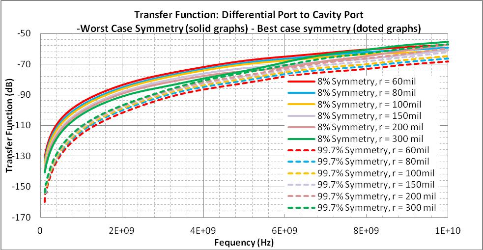
18 Common Mode Voltage on Differential Pair Due to In-Pair Skew 2 Gb/s with 50 ps Rise and Fall Time (+/- 1.0 volts) ps 20 ps 50 ps 100 ps 150 ps 200 ps Level (dbuv) E E E E E E E E E E E+10 Frequency (Hz) 18
19 Extra Skew from Close Proximity to Plane Edge 1 cm Microstrip (5 mil wide, 3 mil height, 1/2 oz) Skew (ps/cm) Distance From Reference Plane Edge (mils) 19
20 18 Percentage of Unit Interval Additional Skew Created From Close Proximity to Edge of Ground-Reference Plane % of UI cm 1 trace width from edge 4 cm 2 trace width from edge Date Rate (Gb/s) 20
21 Rise/Fall Time Mismatch Small amounts of mismatch create significant CM noise Not as significant as skew, but harder to control! Causes Charge/discharge time within IC/ASIC 21
22 0.6 Example of Effect for Differential Signal with Rise/Fall Time Mismatch 2 Gb/s Square Wave (Rise/Fall = 50 & 100 ps) 0.4 Channel 1 Channel 2 T/R=50/100ps 0.2 Voltage E E E E E E E E E E E-09 Time (Seconds) 22
23 Common Mode Voltage on Differential Pair Due to Rise/Fall Time Mismatch 2 Gb/s with Differential Signal +/- 1.0 Volts T/R=50/100ps T/R=50/150ps T/R=50/200ps Level (volts) E-10 1E E-09 2E E-09 3E E-09 4E E-09 5E-09 Time (seconds) 23
24 100 Common Mode Voltage on Differential Pair Due to Rise/Fall Time Mismatch 2 Gb/s with Differential Signal +/- 1.0 Volts T/R=50/55ps T/R=50/100ps T/R=50/150ps T/R=50/200ps Level (dbuv) E E E E E E+10 Frequency (Hz) 24
25 Amplitude Mismatch Small amounts of mismatch create significant CM noise Harmonics are additive with other sources of CM noise Causes Typically imbalance within ASIC/IC 25
26 Common Mode Voltage on Differential Pair Due to Amplitude Mismatch Clock 2 Gb/s with (100 ps Rise/Fall Time) Nominal Differential Signal +/- 1.0 V Amplitude (volts) mv Mismatch 25 mv Mismatch 50 mv Mismatch 100 mv Mismatch 150 mv Mismatch E E E E E E E E E E E-09 Time (Seconds) 26
27 90 Common Mode Voltage on Differential Pair Due to Amplitude Mismatch Clock 2 Gb/s with (100 ps Rise/Fall Time) Nominal Differential Signal +/- 1.0 Volts mv Mismatch 25 mv Mismatch 50 mv Mismatch 100 mv Mismatch 150 mv Mismatch Level (dbuv) E E E E E E E E E E E+10 Frequency (Hz) 27
28 Common Mode from Via Asymmetry Significant CM created! Top View Side View Signal Vias 50 mils GND Via Signal Vias GND Via 28
29 Differential to Single Ended Via Mode Conversion Due to GND Via Asymmetry (In Line) 10 mils between planes Transfer Function (db) mils 100 mils 200 mils 500 mils 1000 mils 2000 mils 3000 mils 50 mils w/ perfect symetry E E E E+11 Frequency (Hz) 29
30 Differential to Single Ended Via Mode Conversion Due to GND Via Asymmetry (In Line) 10 mils between planes (Eleven Planes with Through Via) 0-20 Transfer Function (db) mils 100 mils 200 mils 500 mils 1000 mils 2000 mils 3000 mils E E E E+11 Frequency (Hz) 30


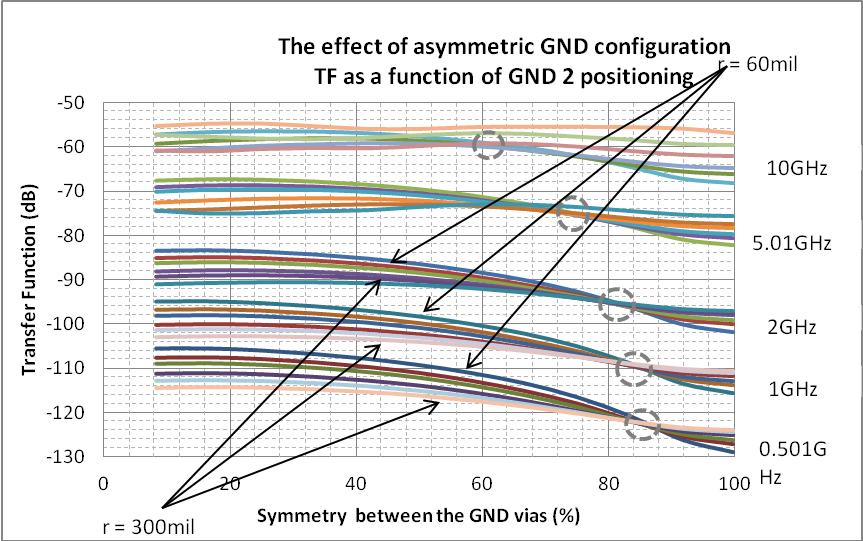
31 Via Symmetry Effect on Common Mode Conversion 31
32 Top View of the Board: Different GND configurations deg deg deg 20 mils deg deg SIG2 PORT 1+ / mils deg deg 20 mils SIG1 PORT 1- / 2- PORT 3 GND mils X 1/17/


33 Asymmetric Ground Via Effects 33 1/17/

34 Asymmetry with Two GND Vias 34
35 35
36 36
37 37
38 38
39 39
40 40
41 Common Mode is Impossible to Avoid Many other asymmetries can add to common mode noise creation Differential pair routed near edge of plane Dielectric effects For EMI, small amounts of CM noise is significant! Above 1 GHz, 1 mv of CM noise is risky! 1mV = 60 dbuv CM filters are required if cables not heavily shielded 41

42 Board-to-Board Differential Pair Issues PCB Plane 2 Microstrip Connector Microstrip V Ground-to-Ground noise PCB Plane 1 42
 Individual Differential Signals ADDED Common Mode Noise 170 mv")
43 Example Measured Differential Individual Signal-to-GND 500 mv P-P (each) Individual Differential Signals ADDED Common Mode Noise 170 mv P-P 43

44 Measured GND-to-GND Voltage 205 mv P-P 44
45 Antenna Structures Dipole antenna Non-Dipole antenna PCB GND planes 45
46 Pin Assignment Controls Inductance for CM signals nh nh (a) (b) nh nh (c) (d) Signal Pin Related Ground Pins 46
47 Connector Pin Assignment Different pins within same pair may have different loop Inductance for CM Ground pins Differential pair pin nH pin nH pin nH pin nH 47
48 Summary Real-world differential signals still have currents in ground-reference planes Differential signals WILL have common mode noise Care is needed to minimize common mode noise Common mode noise causes EMC issues on external cables and between boards In-pair skew, rise/fall time mismatch, amplitude mismatch, and physical channel asymmetry cause common mode noise GND via asymmetry Trace close to edge of ground-reference plane Dielectric weave effects 48
Predicting and Controlling Common Mode Noise from High Speed Differential Signals
 Predicting and Controlling Common Mode Noise from High Speed Differential Signals Bruce Archambeault, Ph.D. IEEE Fellow, inarte Certified Master EMC Design Engineer, Missouri University of Science & Technology
Differential Signaling is the Opiate of the Masses
 Differential Signaling is the Opiate of the Masses Sam Connor Distinguished Lecturer for the IEEE EMC Society 2012-13 IBM Systems & Technology Group, Research Triangle Park, NC My Background BSEE, University
The Ground Myth IEEE. Bruce Archambeault, Ph.D. IBM Distinguished Engineer, IEEE Fellow 18 November 2008
 The Ground Myth Bruce Archambeault, Ph.D. IBM Distinguished Engineer, IEEE Fellow barch@us.ibm.com 18 November 2008 IEEE Introduction Electromagnetics can be scary Universities LOVE messy math EM is not
DEPARTMENT FOR CONTINUING EDUCATION
 DEPARTMENT FOR CONTINUING EDUCATION Reduce EMI Emissions for FREE! by Bruce Archambeault, Ph.D. (reprinted with permission from Bruce Archambeault) Bruce Archambeault presents two courses during the University
EMI. Chris Herrick. Applications Engineer
 Fundamentals of EMI Chris Herrick Ansoft Applications Engineer Three Basic Elements of EMC Conduction Coupling process EMI source Emission Space & Field Conductive Capacitive Inductive Radiative Low, Middle
Frequently Asked EMC Questions (and Answers)
") Frequently Asked EMC Questions (and Answers) Elya B. Joffe President Elect IEEE EMC Society e-mail: eb.joffe@ieee.org December 2, 2006 1 I think I know what the problem is 2 Top 10 EMC Questions 10, 9
Frequently Asked EMC Questions (and Answers) Elya B. Joffe President Elect IEEE EMC Society e-mail: eb.joffe@ieee.org December 2, 2006 1 I think I know what the problem is 2 Top 10 EMC Questions 10, 9
EDA365. DesignCon 2008
 DesignCon 2008 The Impact of Common Mode Currents and Interconnect Inductance on the Signal Quality of Differential Signals in Multi-Board PCB Systems Samuel Connor, IBM sconnor@us.ibm.com Dr. Bhyrav Mutnury,
Chapter 12 Digital Circuit Radiation. Electromagnetic Compatibility Engineering. by Henry W. Ott
 Chapter 12 Digital Circuit Radiation Electromagnetic Compatibility Engineering by Henry W. Ott Forward Emission control should be treated as a design problem from the start, it should receive the necessary
Relationship Between Signal Integrity and EMC
 Relationship Between Signal Integrity and EMC Presented by Hasnain Syed Solectron USA, Inc. RTP, North Carolina Email: HasnainSyed@solectron.com 06/05/2007 Hasnain Syed 1 What is Signal Integrity (SI)?
Low Jitter, Low Emission Timing Solutions For High Speed Digital Systems. A Design Methodology
 Low Jitter, Low Emission Timing Solutions For High Speed Digital Systems A Design Methodology The Challenges of High Speed Digital Clock Design In high speed applications, the faster the signal moves through
Advanced Transmission Lines. Transmission Line 1
 Advanced Transmission Lines Transmission Line 1 Transmission Line 2 1. Transmission Line Theory :series resistance per unit length in. :series inductance per unit length in. :shunt conductance per unit
Near-Field Scanning. Searching for Root Causes
 Near-Field Scanning Searching for Root Causes Feb. 06, 2018 Outline Susceptibility Scanning Conducted susceptibility: where does ESD current go? Near-field effects of electrostatic discharge events Emission
Modeling of EM1 Emissions from Microstrip Structures with Imperfect Reference Planes
 Modeling of EM1 Emissions from Microstrip Structures with Imperfect Reference Planes Bruce Archambeault IBM Raleigh, N.C. Introduction The EM1 radiated emissions from most all commercial electronic products
Electromagnetic Band Gap Structure for Common Mode Filtering of High Speed Differential Signals
 Electromagnetic Band Gap Structure for Common Mode Filtering of High Speed Differential Signals Bruce Archambeault, PhD IEEE Fellow, Missouri University of Science and Technology Adjunct Professor IBM
The number of layers The number and types of planes (power and/or ground) The ordering or sequence of the layers The spacing between the layers
 The ordering or sequence of the layers The spacing between the layers") PCB Layer Stackup PCB layer stackup (the ordering of the layers and the layer spacing) is an important factor in determining the EMC performance of a product. The following four factors are important with
PCB Layer Stackup PCB layer stackup (the ordering of the layers and the layer spacing) is an important factor in determining the EMC performance of a product. The following four factors are important with
ECE 497 JS Lecture - 22 Timing & Signaling
 ECE 497 JS Lecture - 22 Timing & Signaling Spring 2004 Jose E. Schutt-Aine Electrical & Computer Engineering University of Illinois jose@emlab.uiuc.edu 1 Announcements - Signaling Techniques (4/27) - Signaling
Top Ten EMC Problems & EMC Troubleshooting Techniques by Kenneth Wyatt, DVD, Colorado Springs Rev. 1, Feb 26, 2007
 EMC Engineering Top Ten EMC Problems & EMC Troubleshooting Techniques by Kenneth Wyatt, DVD, Colorado Springs Rev. 1, Feb 26, 2007 1a. Ground Impedance The overwhelming majority of high-frequency problems,
Texas Instruments DisplayPort Design Guide
 Texas Instruments DisplayPort Design Guide April 2009 1 High Speed Interface Applications Introduction This application note presents design guidelines, helping users of Texas Instruments DisplayPort devices
Microcircuit Electrical Issues
 Microcircuit Electrical Issues Distortion The frequency at which transmitted power has dropped to 50 percent of the injected power is called the "3 db" point and is used to define the bandwidth of the
Course Introduction Purpose Objectives Content Learning Time
 Course Introduction Purpose This course discusses techniques for analyzing and eliminating noise in microcontroller (MCU) and microprocessor (MPU) based embedded systems. Objectives Learn about a method
PCB Design Techniques for the SI and EMC of Gb/s Differential Transmission Lines
 Abstract PCB Design Techniques for the SI and EMC of Gb/s Differential Transmission Lines By EurIng Keith Armstrong, C.Eng, MIET, MIEEE, www.cherryclough.com Differential transmission lines are becoming
MICTOR. High-Speed Stacking Connector
 MICTOR High-Speed Stacking Connector Electrical Performance Report for the 0.260" (6.6-mm) Stack Height Connector.......... Connector With Typical Footprint................... Connector in a System Report
DDR4 memory interface: Solving PCB design challenges
 DDR4 memory interface: Solving PCB design challenges Chang Fei Yee - July 23, 2014 Introduction DDR SDRAM technology has reached its 4th generation. The DDR4 SDRAM interface achieves a maximum data rate
Effective Routing of Multiple Loads
 feature column BEYOND DESIGN Effective Routing of Multiple Loads by Barry Olney In a previous Beyond Design, Impedance Matching: Terminations, I discussed various termination strategies and concluded that
Keysight Technologies Signal Integrity Tips and Techniques Using TDR, VNA and Modeling
 Keysight Technologies Signal Integrity Tips and Techniques Using, VNA and Modeling Article Reprint This article first appeared in the March 216 edition of Microwave Journal. Reprinted with kind permission
Designing Your EMI Filter
 The Engineer s Guide to Designing Your EMI Filter TABLE OF CONTENTS Introduction Filter Classifications Why Do We Need EMI Filters Filter Configurations 2 2 3 3 How to Determine Which Configuration to
High Speed Clock Distribution Design Techniques for CDC 509/516/2509/2510/2516
 High Speed Clock Distribution Design Techniques for CDC 509/516/2509/2510/2516 APPLICATION REPORT: SLMA003A Boyd Barrie Bus Solutions Mixed Signals DSP Solutions September 1998 IMPORTANT NOTICE Texas Instruments
Design for Guaranteed EMC Compliance
 Clemson Vehicular Electronics Laboratory Reliable Automotive Electronics Automotive EMC Workshop April 29, 2013 Design for Guaranteed EMC Compliance Todd Hubing Clemson University EMC Requirements and
Technical Report Printed Circuit Board Decoupling Capacitor Performance For Optimum EMC Design
 Technical Report Printed Circuit Board Decoupling Capacitor Performance For Optimum EMC Design Bruce Archambeault, Ph.D. Doug White Personal Systems Group Electromagnetic Compatibility Center of Competency
Class-D Audio Power Amplifiers: PCB Layout For Audio Quality, EMC & Thermal Success (Home Entertainment Devices)
") Class-D Audio Power Amplifiers: PCB Layout For Audio Quality, EMC & Thermal Success (Home Entertainment Devices) Stephen Crump http://e2e.ti.com Audio Power Amplifier Applications Audio and Imaging Products
Class-D Audio Power Amplifiers: PCB Layout For Audio Quality, EMC & Thermal Success (Home Entertainment Devices) Stephen Crump http://e2e.ti.com Audio Power Amplifier Applications Audio and Imaging Products
DL-150 The Ten Habits of Highly Successful Designers. or Design for Speed: A Designer s Survival Guide to Signal Integrity
 Slide -1 Ten Habits of Highly Successful Board Designers or Design for Speed: A Designer s Survival Guide to Signal Integrity with Dr. Eric Bogatin, Signal Integrity Evangelist, Bogatin Enterprises, www.bethesignal.com
How to anticipate Signal Integrity Issues: Improve my Channel Simulation by using Electromagnetic based model
 How to anticipate Signal Integrity Issues: Improve my Channel Simulation by using Electromagnetic based model HSD Strategic Intent Provide the industry s premier HSD EDA software. Integration of premier
Q2 QMS-DP/QFS-DP Series 11 mm Stack Height Final Inch Designs in Serial ATA Generation 1 Applications. Revision Date: February 22, 2005
 Q2 QMS-DP/QFS-DP Series 11 mm Stack Height Final Inch Designs in Serial ATA Generation 1 Applications Revision Date: February 22, 2005 Copyrights and Trademarks Copyright 2005 Samtec, Inc. Developed in
Chapter 16 PCB Layout and Stackup
 Chapter 16 PCB Layout and Stackup Electromagnetic Compatibility Engineering by Henry W. Ott Foreword The PCB represents the physical implementation of the schematic. The proper design and layout of a printed
Intel 82566/82562V Layout Checklist (version 1.0)
") Intel 82566/82562V Layout Checklist (version 1.0) Project Name Fab Revision Date Designer Intel Contact SECTION CHECK ITEMS REMARKS DONE General Ethernet Controller Obtain the most recent product documentation
Intel 82566/82562V Layout Checklist (version 1.0) Project Name Fab Revision Date Designer Intel Contact SECTION CHECK ITEMS REMARKS DONE General Ethernet Controller Obtain the most recent product documentation
PCB Design Guidelines for GPS chipset designs. Section 1. Section 2. Section 3. Section 4. Section 5
 PCB Design Guidelines for GPS chipset designs The main sections of this white paper are laid out follows: Section 1 Introduction Section 2 RF Design Issues Section 3 Sirf Receiver layout guidelines Section
Common myths, fallacies and misconceptions in Electromagnetic Compatibility and their correction.
 Common myths, fallacies and misconceptions in Electromagnetic Compatibility and their correction. D. A. Weston EMC Consulting Inc 22-3-2010 These are some of the commonly held beliefs about EMC which are
Differential Signaling
 Differential Signaling Ruey-Beei Wu Rm. 340, Department of Electrical Engineering E-mail: rbwu@ew.ee.ntu.edu.tw url: cc.ee.ntu.edu.tw/~rbwu S. H. Hall et al., High-Speed Digital Designs, Chap.7 1 What
BIRD 74 - recap. April 7, Minor revisions Jan. 22, 2009
 BIRD 74 - recap April 7, 2003 Minor revisions Jan. 22, 2009 Please direct comments, questions to the author listed below: Guy de Burgh, EM Integrity mail to: gdeburgh@nc.rr.com (919) 457-6050 Copyright
HOW SMALL PCB DESIGN TEAMS CAN SOLVE HIGH-SPEED DESIGN CHALLENGES WITH DESIGN RULE CHECKING MENTOR GRAPHICS
 HOW SMALL PCB DESIGN TEAMS CAN SOLVE HIGH-SPEED DESIGN CHALLENGES WITH DESIGN RULE CHECKING MENTOR GRAPHICS H I G H S P E E D D E S I G N W H I T E P A P E R w w w. p a d s. c o m INTRODUCTION Coping with
DP Array DPAM/DPAF Final Inch Designs in Serial ATA Generation 1 Applications 10mm Stack Height. REVISION DATE: January 11, 2005
 Application Note DP Array DPAM/DPAF Final Inch Designs in Serial ATA Generation 1 Applications 10mm Stack Height REVISION DATE: January 11, 2005 Copyrights and Trademarks Copyright 2005 Samtec, Inc. Developed
High Speed Characterization Report
 SSW-1XX-22-X-D-VS Mates with TSM-1XX-1-X-DV-X Description: Surface Mount Terminal Strip,.1 [2.54mm] Pitch, 13.59mm (.535 ) Stack Height Samtec, Inc. 25 All Rights Reserved Table of Contents Connector Overview...
x-mgc Part Number: FCU-022M101
 x-mgc Part Number: FCU-022M101 Features Compliant with IEEE802.3ak (10GBASE-CX4) X2 MSA Rev 1.0b Compatible module Industry standard electrical connector, microgigacn TM (I/O interface) XAUI Four channel
DesignCon Power Distribution Planes: To Split or Not to Split? Technical panel: Bruce Archambeault. Michael Steinberger.
 DesignCon 2009 Technical panel: Power Distribution Planes: To Split or Not to Split? Panelists: Bruce Archambeault Eric Bogatin Michael Steinberger Madhavan Swaminathan Istvan Novak* IBM Bogatin Enterprises
Eye Diagrams. EE290C Spring Most Basic Link BER. What About That Wire. Why Wouldn t You Get What You Sent?
 EE29C Spring 2 Lecture 2: High-Speed Link Overview and Environment Eye Diagrams V V t b This is a This is a V e Eye Opening - space between and Elad Alon Dept. of EECS t e With voltage noise With timing
RiseUp RU8-DP-DV Series 19mm Stack Height Final Inch Designs in Serial ATA Generation 1 Applications. Revision Date: March 18, 2005
 RiseUp RU8-DP-DV Series 19mm Stack Height Final Inch Designs in Serial ATA Generation 1 Applications Revision Date: March 18, 2005 Copyrights and Trademarks Copyright 2005 Samtec, Inc. Developed in conjunction
EE290C Spring Lecture 2: High-Speed Link Overview and Environment. Elad Alon Dept. of EECS
 EE290C Spring 2011 Lecture 2: High-Speed Link Overview and Environment Elad Alon Dept. of EECS Most Basic Link Keep in mind that your goal is to receive the same bits that were sent EE290C Lecture 2 2
Signal Integrity, Part 1 of 3
 by Barry Olney feature column BEYOND DESIGN Signal Integrity, Part 1 of 3 As system performance increases, the PCB designer s challenges become more complex. The impact of lower core voltages, high frequencies
LVDS Owner s Manual. A General Design Guide for National s Low Voltage Differential Signaling (LVDS) Products. Moving Info with LVDS
 Products. Moving Info with LVDS") LVDS Owner s Manual A General Design Guide for National s Low Voltage Differential Signaling (LVDS) Products Moving Info with LVDS Revision 2.0 January 2000 LVDS Evaluation Boards Chapter 6 6.0.0 LVDS
LVDS Owner s Manual A General Design Guide for National s Low Voltage Differential Signaling (LVDS) Products Moving Info with LVDS Revision 2.0 January 2000 LVDS Evaluation Boards Chapter 6 6.0.0 LVDS
VLSI is scaling faster than number of interface pins
 High Speed Digital Signals Why Study High Speed Digital Signals Speeds of processors and signaling Doubled with last few years Already at 1-3 GHz microprocessors Early stages of terahertz Higher speeds
LVDS Flow Through Evaluation Boards. LVDS47/48EVK Revision 1.0
 LVDS Flow Through Evaluation Boards LVDS47/48EVK Revision 1.0 January 2000 6.0.0 LVDS Flow Through Evaluation Boards 6.1.0 The Flow Through LVDS Evaluation Board The Flow Through LVDS Evaluation Board
Differential Signal and Common Mode Signal in Time Domain
 Differential Signal and Common Mode Signal in Time Domain Most of multi-gbps IO technologies use differential signaling, and their typical signal path impedance is ohm differential. Two 5ohm cables, however,
EMC Simulation of Consumer Electronic Devices
 of Consumer Electronic Devices By Andreas Barchanski Describing a workflow for the EMC simulation of a wireless router, using techniques that can be applied to a wide range of consumer electronic devices.
Application Note 5044
 HBCU-5710R 1000BASE-T Small Form Pluggable Low Voltage (3.3V) Electrical Transceiver over Category 5 Unshielded Twisted Pair Cable Characterization Report Application Note 5044 Summary The Physical Medium
The Challenges of Differential Bus Design
 The Challenges of Differential Bus Design February 20, 2002 presented by: Arthur Fraser TechKnowledge Page 1 Introduction Background Historically, differential interconnects were often twisted wire pairs
A NEW COMMON-MODE VOLTAGE PROBE FOR PREDICTING EMI FROM UNSHIELDED DIFFERENTIAL-PAIR CABLES
 A NEW COMMON-MODE VOLTAGE PROBE FOR PREDICTING EMI FROM UNSHIELDED DIFFERENTIAL-PAIR CABLES Neven Pischl Bay Networks Division of Nortel Networks Santa Clara, CA npischl@nortelnetworks.com (408) 495 3261
Plane Crazy, Part 2 BEYOND DESIGN. by Barry Olney
 by Barry Olney column BEYOND DESIGN Plane Crazy, Part 2 In my recent four-part series on stackup planning, I described the best configurations for various stackup requirements. But I did not have the opportunity
PCB. Electromagnetic radiation due to high speed logic from different PCB layouts. (First Draft)
") EMC CONSULTING INC. P.O. Box 496, Merrickville, Ontario, K0G 1N0 Phone: (613) 269-4247 Fax: (613) 269-2045 E-mail: emccons@magma.ca Web Page: www.emcconsultinginc.com PCB. Electromagnetic radiation due
EMC CONSULTING INC. P.O. Box 496, Merrickville, Ontario, K0G 1N0 Phone: (613) 269-4247 Fax: (613) 269-2045 E-mail: emccons@magma.ca Web Page: www.emcconsultinginc.com PCB. Electromagnetic radiation due
QPairs QTE-DP/QSE-DP Final Inch Designs in Serial ATA Generation 1 Applications 5mm Stack Height. REVISION DATE: January 12, 2005
 Application Note QPairs QTE-DP/QSE-DP Final Inch Designs in Serial ATA Generation 1 Applications 5mm Stack Height REVISION DATE: January 12, 2005 Copyrights and Trademarks Copyright 2005 Samtec, Inc. Developed
LoopBack Relay. GLB363 Series. With Built-in AC Bypass Capacitors / DC LoopBack Relay
 GLB363 Series With Built-in AC Bypass Capacitors / DC SERIES DESIGNATION GLB363 RELAY TYPE, Sensitive Coil, Surface Mount Ground Shield and Stub pins with AC Bypass Capacitors or No capacitor DESCRIPTION
Signal Integrity Tips and Techniques Using TDR, VNA and Modeling. Russ Kramer O.J. Danzy
 Signal Integrity Tips and Techniques Using TDR, VNA and Modeling Russ Kramer O.J. Danzy Simulation What is the Signal Integrity Challenge? Tx Rx Channel Asfiakhan Dreamstime.com - 3d People Communication
11 Myths of EMI/EMC ORBEL.COM. Exploring common misconceptions and clarifying them. MYTH #1: EMI/EMC is black magic.
 11 Myths of EMI/EMC Exploring common misconceptions and clarifying them By Ed Nakauchi, Technical Consultant, Orbel Corporation What is a myth? A myth is defined as a popular belief or tradition that has
Design Considerations for High-Speed RS-485 Data Links
 Design Considerations for High-Speed RS-485 Data Links Introduction The trend in high-speed data networks continues to push for higher data rates over longer transmission distances, and under ever-harsher
Matched Length Matched Delay
 by Barry Olney column BEYOND DESIGN Matched Delay In previous columns, I have discussed matched length routing and how matched length does not necessarily mean matched delay. But, all design rules, specified
Effectively Using the EM 6992 Near Field Probe Kit to Troubleshoot EMI Issues
 Effectively Using the EM 6992 Near Field Probe Kit to Troubleshoot EMI Issues Introduction The EM 6992 Probe Kit includes three magnetic (H) field and two electric (E) field passive, near field probes
Optimization of Wafer Level Test Hardware using Signal Integrity Simulation
 June 7-10, 2009 San Diego, CA Optimization of Wafer Level Test Hardware using Signal Integrity Simulation Jason Mroczkowski Ryan Satrom Agenda Industry Drivers Wafer Scale Test Interface Simulation Simulation
A VIEW OF ELECTROMAGNETIC LIFE ABOVE 100 MHz
 A VIEW OF ELECTROMAGNETIC LIFE ABOVE 100 MHz An Experimentalist's Intuitive Approach Lothar O. (Bud) Hoeft, PhD Consultant, Electromagnetic Effects 5012 San Pedro Ct., NE Albuquerque, NM 87109-2515 (505)
High Speed Characterization Report
 QTH-030-01-L-D-A Mates with QSH-030-01-L-D-A Description: High Speed Ground Plane Header Board-to-Board, 0.5mm (.0197 ) Pitch, 5mm (.1969 ) Stack Height Samtec, Inc. 2005 All Rights Reserved Table of Contents
1. TABLE OF FIGURES APPLICATION NOTE OVERVIEW EMI...5
 APPLICATION NOTE 8.7 Rev 1.0 General Guidelines for Reduced Electromagnetic Interference utilizing the SMSC LAN83C175 EPIC 10/100 Mbps Ethernet Controller and Physical Layer Devices By Thomas Greene and
Features. = +25 C, 50 Ohm System, Vcc= 5V
 Typical Applications Prescaler for 1 MHz to 13 GHz PLL Applications: Point-to-Point / Multi-Point Radios VSAT Radios Fiber Optic Test Equipment Space & Military Functional Diagram Features Ultra Low ssb
ITG Electronics, Inc.
 Mitigating EMI Problems & Filter Selection By Rafik Stepanian EMI Noise Generators A change of state (On/Off ) in an Electronic component has the potential to generate EMI. Typical examples are Electronic
PI3DPX1207B Layout Guideline. Table of Contents. 1 Layout Design Guideline Power and GROUND High-speed Signal Routing...
 PI3DPX1207B Layout Guideline Table of Contents 1 Layout Design Guideline... 2 1.1 Power and GROUND... 2 1.2 High-speed Signal Routing... 3 2 PI3DPX1207B EVB layout... 8 3 Related Reference... 8 Page 1
Adjusting Signal Timing (Part 1)
") TECHNICAL PUBLICATION Adjusting Signal Timing (Part 1) Douglas Brooks, President UltraCAD Design, Inc. October 2003 www.mentor.com ABSTRACT It is becoming a routine requirement for PCB designers to tune
TECHNICAL PUBLICATION Adjusting Signal Timing (Part 1) Douglas Brooks, President UltraCAD Design, Inc. October 2003 www.mentor.com ABSTRACT It is becoming a routine requirement for PCB designers to tune
Z-Dok High-Performance Docking Connector
 Z-Dok High-Performance Docking Connector Electrical Performance Report... Connector With Typical Footprint... Connector in a System Report #22GC007, Revision A May 2002 2002 Tyco Electronics, Inc., Harrisburg,
IEEE CX4 Quantitative Analysis of Return-Loss
 IEEE CX4 Quantitative Analysis of Return-Loss Aaron Buchwald & Howard Baumer Mar 003 Return Loss Issues for IEEE 0G-Base-CX4 Realizable Is the spec realizable with standard packages and I/O structures
RESISTIVE POWER SPLITTERS AND DIVIDERS
 RESISTIVE POWER SPLITTERS AND DIVIDERS DC 40.0 GHz S Resistive Power Splitters Usage: : Use in RF and wireless applications where one of the two outputs are included in a leveling loop or used as a reference
H19- Reliable Serial Backplane Data Transmission at 10 Gb/s. January 30, 2002 Slide 1 of 24
 H19- Reliable Serial Backplane Data Transmission at 10 Gb/s Slide 1 of 24 Evolution of the Interconnect F r e q u e n c y A c t i v e Channel Architecture Connectors Transmission Media Loss Properties
Validation Report Comparison of Eye Patterns Generated By Synopsys HSPICE and the Agilent PLTS
 Comparison of Eye Patterns Generated By Synopsys HSPICE and the Agilent PLTS Using: Final Inch Test/Eval Kit, Differential Pair - No Grounds Configuration, QTE-DP/QSE-DP, 5mm Stack Height (P/N FIK-QxE-04-01)
Advanced Topics in EMC Design. Issue 1: The ground plane to split or not to split?
 NEEDS 2006 workshop Advanced Topics in EMC Design Tim Williams Elmac Services C o n s u l t a n c y a n d t r a i n i n g i n e l e c t r o m a g n e t i c c o m p a t i b i l i t y e-mail timw@elmac.co.uk
PHY DESIGN RECOMMENDATIONS FOR PCB LAYOUT
 PHY DESIGN RECOMMENDATIONS FOR PCB LAYOUT Ron Raybarman s-raybarman1@ti ti.com Texas Instruments Topics of discussion: 1. Specific for 1394 - (Not generic PCB layout) Etch lengths Termination Network Skew
Taking the Mystery out of Signal Integrity
 Slide - 1 Jan 2002 Taking the Mystery out of Signal Integrity Dr. Eric Bogatin, CTO, GigaTest Labs Signal Integrity Engineering and Training 134 S. Wolfe Rd Sunnyvale, CA 94086 408-524-2700 www.gigatest.com
Suppression Techniques using X2Y as a Broadband EMI Filter IEEE International Symposium on EMC, Boston, MA
 Suppression Techniques using X2Y as a Broadband EMI Filter Jim Muccioli Tony Anthony Dave Anthony Dale Sanders X2Y Attenuators, LLC Erie, PA 16506-2972 www.x2y.com Email: x2y@x2y.com Bart Bouma Yageo/Phycomp
Differential Pair Routing
 C O L U M N BEYOND DESIGN Differential Pair Routing by Barry Olney IN-CIRCUIT DESIGN PTY LTD, AUSTRALIA A differential pair is two complementary transmission lines that transfer equal and opposite signals
Ensuring Signal and Power Integrity for High-Speed Digital Systems
 Ensuring Signal and Power Integrity for High-Speed Digital Systems An EMC Perspective Christian Schuster Institut für Theoretische Elektrotechnik Technische Universität Hamburg-Harburg (TUHH) Invited Presentation
PCI-EXPRESS CLOCK SOURCE. Features
 DATASHEET ICS557-01 Description The ICS557-01 is a clock chip designed for use in PCI-Express Cards as a clock source. It provides a pair of differential outputs at 100 MHz in a small 8-pin SOIC package.
AltiumLive 2017: Component selection for EMC
 AltiumLive 2017: Component selection for EMC Martin O Hara Victory Lighting Ltd Munich, 24-25 October 2017 Component Selection Passives resistors, capacitors and inductors Discrete diodes, bipolar transistors,
A Novel Embedded Common-mode Filter for above GHz differential signals based on Metamaterial concept. Tzong-Lin Wu
 c //3 A Novel Embedded Common-mode Filter for above GHz differential signals based on Metamaterial concept Tzong-Lin Wu Professor Graduate Institute of Communication Engineering, National Taiwan University,
ECE Microwave Engineering
 ECE 5317-6351 Microwave Engineering Adapted from notes by Prof. Jeffery T. Williams Fall 2018 Prof. David R. Jackson Dept. of ECE Notes 4 Transmission Lines Part 3: Baluns 1 Baluns Baluns are used to connect
CFORTH-X2-10GB-CX4 Specifications Rev. D00A
 CFORTH-X2-10GB-CX4 Specifications Rev. D00A Preliminary DATA SHEET CFORTH-X2-10GB-CX4 10GBASE-CX4 X2 Transceiver CFORTH-X2-10GB-CX4 Overview CFORTH-X2-10GB-CX4 10GBd X2 Electrical transceivers are designed
DesignCon Design of Gb/s Interconnect for High-bandwidth FPGAs. Sherri Azgomi, Altera Corporation
 DesignCon 2004 Design of 3.125 Gb/s Interconnect for High-bandwidth FPGAs Sherri Azgomi, Altera Corporation sazgomi@altera.com Lawrence Williams, Ph.D., Ansoft Corporation williams@ansoft.com CF-031505-1.0
EMI AND BEL MAGNETIC ICM
 EMI AND BEL MAGNETIC ICM ABSTRACT Electromagnetic interference (EMI) in a local area network (LAN) system is a common problem that every LAN system designer faces, and it is a growing problem because the
Impedance-Controlled Routing. Contents
 Impedance-Controlled Routing Contents Do I Need Impedance Controlled Routing? How do I Control the Impedances? Impedance Matching the Components What Determines the Routing Impedance? Calculating the Routing
Introduction to EMI/EMC Challenges and Their Solution
 Introduction to EMI/EMC Challenges and Their Solution Dr. Hany Fahmy HSD Application Expert Agilent Technologies Davy Pissort, K.U. Leuven Charles Jackson, Nvidia Charlie Shu, Nvidia Chen Wang, Nvidia
Cross Coupling Between Power and Signal Traces on Printed Circuit Boards
 Cross Coupling Between Power and Signal Traces on Printed Circuit Boards Dr. Zorica Pantic-Tanner Edwin Salgado Franz Gisin San Francisco State University Silicon Graphics Inc. Silicon Graphics Inc. 1600
Does skew really degrade SERDES performance?
 DesignCon 2015 Does skew really degrade SERDES performance? Shirin Farrahi, Oracle Corp. Vijay Kunda, Oracle Corp. Ying Li, Oracle Corp. Xun Zhang, Oracle Corp. Gustavo Blando, Oracle Corp. Istvan Novak,
Losses Induced by Asymmetry in Differential Transmission Lines
 DesignCon 27 Losses Induced by Asymmetry in Differential Transmission Lines Gustavo Blando, Sun Microsystems Jason R. Miller, Sun Microsystems Istvan Novak, Sun Microsystems Abstract Even though differential
Brief Overview of EM Computational Modeling Techniques for Real-World Engineering Problems
 Brief Overview of EM Computational Modeling Techniques for Real-World Engineering Problems Bruce Archambeault, Ph.D. IEEE Fellow, IBM Distinguished Engineer Emeritus Bruce@brucearch.com Archambeault EMI/EMC
DL-150 The Ten Habits of Highly Successful Designers. or Design for Speed: A Designer s Survival Guide to Signal Integrity
 Slide -1 Ten Habits of Highly Successful Board Designers or Design for Speed: A Designer s Survival Guide to Signal Integrity with Dr. Eric Bogatin, Signal Integrity Evangelist, Bogatin Enterprises, www.bethesignal.com
Using the CDC857 and CDCV850 to Transform a Single-Ended Clock Signal Into Differential Outputs
 Application Report SCAA043 - September 2000 Using the CDC857 and CDCV850 to Transform a Single-Ended Clock Signal Into Differential Outputs Falk Alicke MSDS Application Team ABSTRACT The CDC857 and the
CROSSTALK DUE TO PERIODIC PLANE CUTOUTS. Jason R. Miller, Gustavo Blando, Istvan Novak Sun Microsystems
 CROSSTALK DUE TO PERIODIC PLANE CUTOUTS Jason R. Miller, Gustavo Blando, Istvan Novak Sun Microsystems 1 Outline 1 Introduction 2 Crosstalk Theory 3 Measurement 4 Simulation correlation 5 Parameterized