Effective Routing of Multiple Loads
|
|
|
- Earl Robertson
- 5 years ago
- Views:
Transcription

1

2 feature column BEYOND DESIGN Effective Routing of Multiple Loads by Barry Olney In a previous Beyond Design, Impedance Matching: Terminations, I discussed various termination strategies and concluded that a series terminator is best for high-speed transmission lines. Different terminating strategies have advantages and disadvantages depending on the application, but in general, series termination is excellent for point-to-point routes, one load per net. In summary, series termination reduces ringing and ground bounce. But, what if there are a number of loads how should these transmission lines be routed? For perfect transfer of energy and to eliminate reflections, the impedance of the source must equal the impedance of the trace(s) to the load. Bifurcated transmission lines traces that are split into two or more T-sections are sometimes used to distribute signals to multiple loads. The impedance of the bifurcated line is not constant along the trace route, as the traces branching from the T-section are virtually in parallel when you consider the equivalent AC circuit. In this case, proper termination has not been provided and an impedance discontinuity can be seen at the branch point. In Figure 1, a 50 ohm signal from the driver is split into two transmission lines of 50 ohms and then into the loads. At branch (A), the two 50 ohm traces in parallel equate to a 25 ohm equivalent trace, and a mismatch in impedance. Figure 2 illustrates the resultant waveform of the unmatched transmission line. Bifurcated transmission lines with matched impedances are a better choice. Rather than having the traces all the same width, the branch traces are reduced in order to match the impedance at the branch. The impedance of the traces after the branch then becomes 2 x Zo or


3 ohms, and since these are in parallel the load seen at the branch is 50 ohms. This would work fairly well if we could just halve the trace width. But, the width of the trace is not directly proportional to the impedance and a field solver is required to calculate the correct width required. For instance, a 24 mil trace of 52 ohms has to drop to 4 mil to double in impedance given the same substrate. This is solved by the ICD Stackup Planner Field Solver in Figure 3. The ICD Stackup Planner can be downloaded from This configuration also requires parallel pull-down resistors of 2 x Zo at each load. These end terminators ensure that the transmitted pulse progresses once down the line and then 32

4 stops preventing reflection which is what impedance matching is all about. Figure 5 illustrates the improved waveform of the matched bifurcated line of Figure 4. This technique, for matching branched lines, is not often used due to the difficulty of fabricating traces of widely varying impedance on the same substrate. Also, space limitations beneath FPGAs limit the width of the thicker trace. Another issue with this technique lies with the loop return currents created within the network. If one of the bifurcated traces is located on a different layer to the other, the return current will be referenced to different planes. When this occurs, a potentially large loop area is created, with a corresponding increase in radiated emissions. GND 33

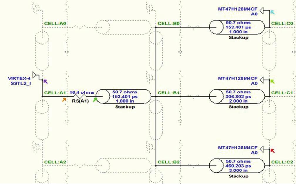
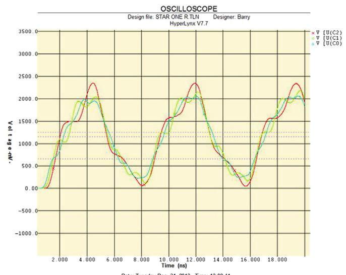
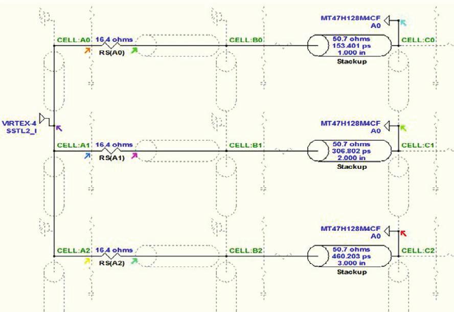
5 stitching vias may help alleviate this problem. We ve covered differential clock and strobe routing in previous columns, but let s look at address routing. Fly-by topology as used in double data rate design uses a daisy-chain or multi-drop topology on address, command and control signals. Fly-by topology reduces simultaneous switching noise (SSN) by deliberately causing flight-time skew between the data and strobes at every chip/ SDRAM requiring controllers to compensate for this skew by adjusting the timing per byte lane. In this case, a series terminator (R11) is employed close to the driver and a parallel 100 ohm VTT pull-up (R18 resistor network) at the end of the loads. If the distance from the source to the first load is short, then the series terminator may not be required. But, this should be determined by simulation. The ideal location for end terminators is past the last load with no side branch or stub as depicted. Stub length should be kept to a minimum. You can see how the address line, highlighted in Figure 6, is routed directly over the memory/load pin with a very short stub going off to each load. Since this stub is extremely short, compared to the transmission line length and length of the rising edge, an impedance mismatch is avoided. Short stubs, and their associated receiver capacitance, act like simple capacitive loads which tend to roll-off the rising edge. This configuration is ideal for DDR design but what if there is a slower rise-time clock that needs to be distributed to a number of loads? Star routing is ideal for distributing clocks to multiple loads and is also used for power distribution on signal layers. The routing fansout from a central point and connects to each load. But, with distributed loads also comes unmatched lengths between the loads. If a single series terminator is used, close to the source as in Figure 7, the different trace lengths cause different delays to each load which is unavoidable unless the lengths are matched. This also creates reflections which can be seen in Figure 8. Reflections occur whenever the impedance of the transmission line changes along its length. This can be caused by unmatched drivers/loads, layer transitions, different dielectric materials, stubs, vias, connectors and IC packages. By understanding the causes of these reflections and eliminating the source of the mismatch, a design can be engineered with reliable performance. In Figure 9, three individual series terminators are used in conjunction with three different trace lengths. Figure 10 illustrates the resultant clean waveform. If all the trace lengths, of the star configuration, are matched to length/delay then these reflections do not occur. So there is a choice: match the lengths or use individual series ter- 34
6 36

7 37


8 minators close to the source to dampen the reflections. Points to Remember transmission lines. are split into two or more T-sections are sometimes used to distribute signals to multiple loads. parallel equate to a 25 ohm equivalent trace and a mismatch in impedance. impedance. impedances are a better choice. mitted pulse progresses once down the line and then stops, preventing reflection. used due to the difficulty of fabricating traces of widely varying impedance on the same substrate. a different layer to the other, the return current will be referenced to different planes potentially creating a large loop area and EMI. tor close to the driver and a parallel 100 ohm VTT pull-up at the end of the loads. to multiple loads and is also used for power distribution on signal layers. routing are unmatched. use individual series terminators, close to the source, to dampen the reflections of a star route. PCBDESIGN References 1. Barry Olney Advanced Design for SMT, Beyond Design: Impedance Matching: Terminations, Beyond Design: Differential Pair Routing, PCB Design Techniques for DDR, DDR2 & DDR3, Part 1, PCB Design Techniques for DDR, DDR2 & DDR3, Part 2 2. Howard Johnson High-Speed Digital Design 3. Mark Montrose EMC and the Printed Circuit Board 4. The ICD Stackup Planner and PDN Planner Energy Harvesting Systems to Reach $375M by 2020 by Real Time with... NEPCON South China. 38
Impedance Matching: Terminations
 by Barry Olney IN-CIRCUIT DESIGN PTY LTD AUSTRALIA column BEYOND DESIGN Impedance Matching: Terminations The impedance of the trace is extremely important, as any mismatch along the transmission path will
Matched Length Matched Delay
 by Barry Olney column BEYOND DESIGN Matched Delay In previous columns, I have discussed matched length routing and how matched length does not necessarily mean matched delay. But, all design rules, specified
Split Planes in Multilayer PCBs
 by Barry Olney coulmn BEYOND DESIGN Split Planes in Multilayer PCBs Creating split planes or isolated islands in the copper planes of multilayer PCBs at first seems like a good idea. Today s high-speed
Signal Integrity, Part 1 of 3
 by Barry Olney feature column BEYOND DESIGN Signal Integrity, Part 1 of 3 As system performance increases, the PCB designer s challenges become more complex. The impact of lower core voltages, high frequencies
Plane Crazy, Part 2 BEYOND DESIGN. by Barry Olney
 by Barry Olney column BEYOND DESIGN Plane Crazy, Part 2 In my recent four-part series on stackup planning, I described the best configurations for various stackup requirements. But I did not have the opportunity
Introduction to Board Level Simulation and the PCB Design Process
 BEYOND DESIGN C O L U M N Introduction to Board Level Simulation and the PCB Design Process by Barry Olney IN-CIRCUIT DESIGN PTY LTD AUSTRALIA SUMMARY Board-level simulation reduces costs by identifying
Differential Pair Routing
 C O L U M N BEYOND DESIGN Differential Pair Routing by Barry Olney IN-CIRCUIT DESIGN PTY LTD, AUSTRALIA A differential pair is two complementary transmission lines that transfer equal and opposite signals
Multilayer PCB Stackup Planning
 by Barry Olney In-Circuit Design Pty Ltd Australia This Application Note details tried and proven techniques for planning high speed Multilayer PCB Stackup configurations. Planning the multilayer PCB stackup
Low Jitter, Low Emission Timing Solutions For High Speed Digital Systems. A Design Methodology
 Low Jitter, Low Emission Timing Solutions For High Speed Digital Systems A Design Methodology The Challenges of High Speed Digital Clock Design In high speed applications, the faster the signal moves through
Learning the Curve BEYOND DESIGN. by Barry Olney
 by Barry Olney coulmn BEYOND DESIGN Learning the Curve Currently, power integrity is just entering the mainstream market phase of the technology adoption life cycle. The early market is dominated by innovators
HOW SMALL PCB DESIGN TEAMS CAN SOLVE HIGH-SPEED DESIGN CHALLENGES WITH DESIGN RULE CHECKING MENTOR GRAPHICS
 HOW SMALL PCB DESIGN TEAMS CAN SOLVE HIGH-SPEED DESIGN CHALLENGES WITH DESIGN RULE CHECKING MENTOR GRAPHICS H I G H S P E E D D E S I G N W H I T E P A P E R w w w. p a d s. c o m INTRODUCTION Coping with
DDR4 memory interface: Solving PCB design challenges
 DDR4 memory interface: Solving PCB design challenges Chang Fei Yee - July 23, 2014 Introduction DDR SDRAM technology has reached its 4th generation. The DDR4 SDRAM interface achieves a maximum data rate
Relationship Between Signal Integrity and EMC
 Relationship Between Signal Integrity and EMC Presented by Hasnain Syed Solectron USA, Inc. RTP, North Carolina Email: HasnainSyed@solectron.com 06/05/2007 Hasnain Syed 1 What is Signal Integrity (SI)?
How to anticipate Signal Integrity Issues: Improve my Channel Simulation by using Electromagnetic based model
 How to anticipate Signal Integrity Issues: Improve my Channel Simulation by using Electromagnetic based model HSD Strategic Intent Provide the industry s premier HSD EDA software. Integration of premier
Faster than a Speeding Bullet
 BEYOND DESIGN Faster than a Speeding Bullet by Barry Olney IN-CIRCUIT DESIGN PTY LTD AUSTRALIA In a previous Beyond Design column, Transmission Lines, I mentioned that a transmission line does not carry
The number of layers The number and types of planes (power and/or ground) The ordering or sequence of the layers The spacing between the layers
 The ordering or sequence of the layers The spacing between the layers") PCB Layer Stackup PCB layer stackup (the ordering of the layers and the layer spacing) is an important factor in determining the EMC performance of a product. The following four factors are important with
PCB Layer Stackup PCB layer stackup (the ordering of the layers and the layer spacing) is an important factor in determining the EMC performance of a product. The following four factors are important with
8. QDR II SRAM Board Design Guidelines
 8. QDR II SRAM Board Design Guidelines November 2012 EMI_DG_007-4.2 EMI_DG_007-4.2 This chapter provides guidelines for you to improve your system's signal integrity and layout guidelines to help successfully
In this pdf file, you can see the most common 7 kinds of multilayer PCB configurations.
 4-16 Layer PCB Stackup In this pdf file, you can see the most common 7 kinds of multilayer PCB configurations. There is really no limit to the number of layers that can be fabricated in a multilayer PCB.
PI3HDMIxxx 4-Layer PCB Layout Guideline for HDMI Products
 PI3HDMIxxx 4-Layer PCB Layout Guideline for HDMI Products Introduction The differential trace impedance of HDMI is specified at 100Ω±15% in Test ID 8-8 in HDMI Compliance Test Specification Rev.1.2a and
Intro. to PDN Planning PCB Stackup Technology Series
 Introduction to Power Distribution Network (PDN) Planning Bill Hargin In-Circuit Design b.hargin@icd.com.au 425-301-4425 Intro. to PDN Planning 1. Intro/Overview 2. Bypass/Decoupling Strategy 3. Plane
Chapter 16 PCB Layout and Stackup
 Chapter 16 PCB Layout and Stackup Electromagnetic Compatibility Engineering by Henry W. Ott Foreword The PCB represents the physical implementation of the schematic. The proper design and layout of a printed
Analysis on the Effectiveness of Clock Trace Termination Methods and Trace Lengths on a Printed Circuit Board
 Analysis on the Effectiveness of Clock Trace Termination Methods and Trace Lengths on a Printed Circuit Board Mark I. Montrose Montrose Compliance Services 2353 Mission Glen Dr. Santa Clara, CA 95051-1214
Microcircuit Electrical Issues
 Microcircuit Electrical Issues Distortion The frequency at which transmitted power has dropped to 50 percent of the injected power is called the "3 db" point and is used to define the bandwidth of the
Texas Instruments DisplayPort Design Guide
 Texas Instruments DisplayPort Design Guide April 2009 1 High Speed Interface Applications Introduction This application note presents design guidelines, helping users of Texas Instruments DisplayPort devices
Section VI. PCB Layout Guidelines
 Section VI. PCB Layout Guidelines This section provides information for board layout designers to successfully layout their boards for Stratix II devices. These chapters contain the required PCB layout
PI3DPX1207B Layout Guideline. Table of Contents. 1 Layout Design Guideline Power and GROUND High-speed Signal Routing...
 PI3DPX1207B Layout Guideline Table of Contents 1 Layout Design Guideline... 2 1.1 Power and GROUND... 2 1.2 High-speed Signal Routing... 3 2 PI3DPX1207B EVB layout... 8 3 Related Reference... 8 Page 1
Effect of slots in reference planes on signal propagation in single and differential t-lines
 Simbeor Application Note #2007_09, November 2007 2007 Simberian Inc. Effect of slots in reference planes on signal propagation in single and differential t-lines Simberian, Inc. www.simberian.com Simbeor:
Modeling System Signal Integrity Uncertainty Considerations
 white paper Intel FPGA Modeling System Signal Integrity Uncertainty Considerations Authors Ravindra Gali High-Speed I/O Applications Engineering, Intel Corporation Zhi Wong High-Speed I/O Applications
Signal/Power Integrity Analysis of High-Speed Memory Module with Meshed Reference Plane 1
 , pp.119-128 http//dx.doi.org/10.14257/ijca.2018.11.7.10 Signal/Power Integrity Analysis of High-Speed Memory Module with Meshed Reference Plane 1 Moonjung Kim Institute of IT Convergence Technology, Dept.
Intel 82566/82562V Layout Checklist (version 1.0)
") Intel 82566/82562V Layout Checklist (version 1.0) Project Name Fab Revision Date Designer Intel Contact SECTION CHECK ITEMS REMARKS DONE General Ethernet Controller Obtain the most recent product documentation
Intel 82566/82562V Layout Checklist (version 1.0) Project Name Fab Revision Date Designer Intel Contact SECTION CHECK ITEMS REMARKS DONE General Ethernet Controller Obtain the most recent product documentation
EMC problems from Common Mode Noise on High Speed Differential Signals
 EMC problems from Common Mode Noise on High Speed Differential Signals Bruce Archambeault, PhD Alma Jaze, Sam Connor, Jay Diepenbrock IBM barch@us.ibm.com 1 Differential Signals Commonly used for high
ALTIUM LIVE 2018: PRACTICAL HIGH-SPEED DESIGN CONSTRAINTS. Randy Clemmons CID+ San Diego PCB October 5, 2018
 ALTIUM LIVE 2018: PRACTICAL HIGH-SPEED DESIGN CONSTRAINTS Randy Clemmons CID+ San Diego PCB October 5, 2018 Technology Boom Cycle Virtual Reality Artificial Intelligence Internet of Things Drones Driverless
High Speed Clock Distribution Design Techniques for CDC 509/516/2509/2510/2516
 High Speed Clock Distribution Design Techniques for CDC 509/516/2509/2510/2516 APPLICATION REPORT: SLMA003A Boyd Barrie Bus Solutions Mixed Signals DSP Solutions September 1998 IMPORTANT NOTICE Texas Instruments
DL-150 The Ten Habits of Highly Successful Designers. or Design for Speed: A Designer s Survival Guide to Signal Integrity
 Slide -1 Ten Habits of Highly Successful Board Designers or Design for Speed: A Designer s Survival Guide to Signal Integrity with Dr. Eric Bogatin, Signal Integrity Evangelist, Bogatin Enterprises, www.bethesignal.com
Signal Technologies 1
 Signal Technologies 1 Gunning Transceiver Logic (GTL) - evolution Evolved from BTL, the backplane transceiver logic, which in turn evolved from ECL (emitter-coupled logic) Setup of an open collector bus
The Ground Myth IEEE. Bruce Archambeault, Ph.D. IBM Distinguished Engineer, IEEE Fellow 18 November 2008
 The Ground Myth Bruce Archambeault, Ph.D. IBM Distinguished Engineer, IEEE Fellow barch@us.ibm.com 18 November 2008 IEEE Introduction Electromagnetics can be scary Universities LOVE messy math EM is not
EMI. Chris Herrick. Applications Engineer
 Fundamentals of EMI Chris Herrick Ansoft Applications Engineer Three Basic Elements of EMC Conduction Coupling process EMI source Emission Space & Field Conductive Capacitive Inductive Radiative Low, Middle
DL-150 The Ten Habits of Highly Successful Designers. or Design for Speed: A Designer s Survival Guide to Signal Integrity
 Slide -1 Ten Habits of Highly Successful Board Designers or Design for Speed: A Designer s Survival Guide to Signal Integrity with Dr. Eric Bogatin, Signal Integrity Evangelist, Bogatin Enterprises, www.bethesignal.com
Taking the Mystery out of Signal Integrity
 Slide - 1 Jan 2002 Taking the Mystery out of Signal Integrity Dr. Eric Bogatin, CTO, GigaTest Labs Signal Integrity Engineering and Training 134 S. Wolfe Rd Sunnyvale, CA 94086 408-524-2700 www.gigatest.com
ICS309 SERIAL PROGRAMMABLE TRIPLE PLL SS VERSACLOCK SYNTH. Description. Features. Block Diagram DATASHEET
 DATASHEET ICS309 Description The ICS309 is a versatile serially-programmable, triple PLL with spread spectrum clock source. The ICS309 can generate any frequency from 250kHz to 200 MHz, and up to 6 different
LVDS Flow Through Evaluation Boards. LVDS47/48EVK Revision 1.0
 LVDS Flow Through Evaluation Boards LVDS47/48EVK Revision 1.0 January 2000 6.0.0 LVDS Flow Through Evaluation Boards 6.1.0 The Flow Through LVDS Evaluation Board The Flow Through LVDS Evaluation Board
HiPerClockS TM Application Note High Speed LVCMOS Driver Termination Design Guide
 This application note provides general design guide for high speed LVCMOS driver termination. To handle high speed LVCMOS drivers, general rules for high-speed digital board design must be carefully followed.
PCB Design Guidelines for Reduced EMI
 PCB Design Guidelines for Reduced EMI Guided By: Prof. Ruchi Gajjar Prepared By: Shukla Jay (13MECE17) Outline Power Distribution for Two-Layer Boards Gridding Power Traces on Two-Layer Boards Ferrite
Eye Diagrams. EE290C Spring Most Basic Link BER. What About That Wire. Why Wouldn t You Get What You Sent?
 EE29C Spring 2 Lecture 2: High-Speed Link Overview and Environment Eye Diagrams V V t b This is a This is a V e Eye Opening - space between and Elad Alon Dept. of EECS t e With voltage noise With timing
EE290C Spring Lecture 2: High-Speed Link Overview and Environment. Elad Alon Dept. of EECS
 EE290C Spring 2011 Lecture 2: High-Speed Link Overview and Environment Elad Alon Dept. of EECS Most Basic Link Keep in mind that your goal is to receive the same bits that were sent EE290C Lecture 2 2
TMS320C6474 DDR2 Implementation Guidelines
 TMS320C6474 Implementation Guidelines Ronald Lerner... ABSTRACT This document provides implementation instructions for the interface contained on the C6474 DSP. Contents 1 Prerequisites... 2 2 C6474 Supported
Advanced Topics in EMC Design. Issue 1: The ground plane to split or not to split?
 NEEDS 2006 workshop Advanced Topics in EMC Design Tim Williams Elmac Services C o n s u l t a n c y a n d t r a i n i n g i n e l e c t r o m a g n e t i c c o m p a t i b i l i t y e-mail timw@elmac.co.uk
High-Speed PCB Design und EMV Minimierung
 TRAINING Bei dem hier beschriebenen Training handelt es sich um ein Cadence Standard Training. Sie erhalten eine Dokumentation in englischer Sprache. Die Trainingssprache ist deutsch, falls nicht anders
Terminating RoboClock II Output
 Cypress Semiconductor White Paper Executive Summary This document describes the methods available for terminating the output for the RoboClock II family of products. It also weighs the benefits of each
The Challenges of Differential Bus Design
 The Challenges of Differential Bus Design February 20, 2002 presented by: Arthur Fraser TechKnowledge Page 1 Introduction Background Historically, differential interconnects were often twisted wire pairs
ECE 497 JS Lecture - 22 Timing & Signaling
 ECE 497 JS Lecture - 22 Timing & Signaling Spring 2004 Jose E. Schutt-Aine Electrical & Computer Engineering University of Illinois jose@emlab.uiuc.edu 1 Announcements - Signaling Techniques (4/27) - Signaling
Cyclone III Simultaneous Switching Noise (SSN) Design Guidelines
 Design Guidelines") Cyclone III Simultaneous Switching Noise (SSN) Design Guidelines December 2007, ver. 1.0 Introduction Application Note 508 Low-cost FPGAs designed on 90-nm and 65-nm process technologies are made to support
Cyclone III Simultaneous Switching Noise (SSN) Design Guidelines December 2007, ver. 1.0 Introduction Application Note 508 Low-cost FPGAs designed on 90-nm and 65-nm process technologies are made to support
TECHNICAL NOTE TN DDR2 DESIGN GUIDE FOR TWO-DIMM SYSTEMS DDR2-533 MEMORY DESIGN GUIDE FOR TWO-DIMM UNBUFFERED SYSTEMS
 TECHNICL NOTE DDR2-533 MEMORY DESIGN GUIDE FOR TWO-DIMM UNBUFFERED SYSTEMS Overview DDR2 memory busses vary depending on the intended market for the finished product. Some products must support four or
Practical Design Considerations for Dense, High-Speed, Differential Stripline PCB Routing Related to Bends, Meanders and Jog-outs
 Practical Design Considerations for Dense, High-Speed, Differential Stripline PCB Routing Related to Bends, Meanders and Jog-outs AUTHORS Michael J. Degerstrom, Mayo Clinic degerstrom.michael@mayo.edu
TD_485 Transceiver Modules Application Guide 2017
 TD_485 Transceiver Modules Application Guide 2017 1. RS485 basic knowledge... 2 1.1. RS485 BUS basic Characteristics... 2 1.2. RS485 Transmission Distance... 2 1.3. RS485 bus connection and termination
MPC5606E: Design for Performance and Electromagnetic Compatibility
 Freescale Semiconductor, Inc. Document Number: AN5100 Application Note MPC5606E: Design for Performance and Electromagnetic Compatibility by: Tomas Kulig 1. Introduction This document provides information
CPS-1848 PCB Design Application Note
 Titl CPS-1848 PCB Design Application Note June 22, 2010 6024 Silver Creek Valley Road, San Jose, California 95138 Telephone: (408) 284-8200 Fax: (408) 284-3572 2010 About this Document This document is
Impedance-Controlled Routing. Contents
 Impedance-Controlled Routing Contents Do I Need Impedance Controlled Routing? How do I Control the Impedances? Impedance Matching the Components What Determines the Routing Impedance? Calculating the Routing
1 Introduction External Component Requirements AC Coupling Capacitors on high speed lanes... 2
 PI3TB212 PI3TB212 Thunderbolt Application Information Table of Contents 1 Introduction... 2 2 External Component Requirements... 2 2.1 AC Coupling Capacitors on high speed lanes... 2 2.2 Pull-down Resistor
Using IBIS Models for Timing Analysis
 Application Report SPRA839A - April 2003 Using IBIS Models for Timing Analysis ABSTRACT C6000 Hardware Applications Today s high-speed interfaces require strict timings and accurate system design. To achieve
Differential Signaling is the Opiate of the Masses
 Differential Signaling is the Opiate of the Masses Sam Connor Distinguished Lecturer for the IEEE EMC Society 2012-13 IBM Systems & Technology Group, Research Triangle Park, NC My Background BSEE, University
Differential-Mode Emissions
 Differential-Mode Emissions In Fig. 13-5, the primary purpose of the capacitor C F, however, is to filter the full-wave rectified ac line voltage. The filter capacitor is therefore a large-value, high-voltage
Introduction to EMI/EMC Challenges and Their Solution
 Introduction to EMI/EMC Challenges and Their Solution Dr. Hany Fahmy HSD Application Expert Agilent Technologies Davy Pissort, K.U. Leuven Charles Jackson, Nvidia Charlie Shu, Nvidia Chen Wang, Nvidia
Application Note. Signal Integrity Modeling. SCSI Connector and Cable Modeling from TDR Measurements
 Application Note SCSI Connector and Cable Modeling from TDR Measurements Signal Integrity Modeling SCSI Connector and Cable Modeling from TDR Measurements Dima Smolyansky TDA Systems, Inc. http://www.tdasystems.com
Digital Systems Power, Speed and Packages II CMPE 650
 Speed VLSI focuses on propagation delay, in contrast to digital systems design which focuses on switching time: A B A B rise time propagation delay Faster switching times introduce problems independent
PHY DESIGN RECOMMENDATIONS FOR PCB LAYOUT
 PHY DESIGN RECOMMENDATIONS FOR PCB LAYOUT Ron Raybarman s-raybarman1@ti ti.com Texas Instruments Topics of discussion: 1. Specific for 1394 - (Not generic PCB layout) Etch lengths Termination Network Skew
Design of optimal differential viaholes for 6-plane board
 Simbeor Application Note #2007_08, October 2007 2007 Simberian Inc. Design of optimal differential viaholes for 6-plane board Simberian, Inc. www.simberian.com Simbeor: Easy-to-Use, Efficient and Cost-Effective
Signal Integrity Tips and Techniques Using TDR, VNA and Modeling. Russ Kramer O.J. Danzy
 Signal Integrity Tips and Techniques Using TDR, VNA and Modeling Russ Kramer O.J. Danzy Simulation What is the Signal Integrity Challenge? Tx Rx Channel Asfiakhan Dreamstime.com - 3d People Communication
APPLICATION NOTE 735 Layout Considerations for Non-Isolated DC-DC Converters
 Maxim > App Notes > AUTOMOTIVE GENERAL ENGINEERING TOPICS POWER-SUPPLY CIRCUITS PROTOTYPING AND PC BOARD LAYOUT Keywords: printed circuit board, PCB layout, parasitic inductance, parasitic capacitance,
PCB Design Guidelines for GPS chipset designs. Section 1. Section 2. Section 3. Section 4. Section 5
 PCB Design Guidelines for GPS chipset designs The main sections of this white paper are laid out follows: Section 1 Introduction Section 2 RF Design Issues Section 3 Sirf Receiver layout guidelines Section
/14/$ IEEE 939
 Electro-Mechanical Structures for Channel Emulation Satyajeet Shinde #1, Sen Yang #2, Nicholas Erickson #3, David Pommerenke #4, Chong Ding *1, Douglas White *1, Stephen Scearce *1, Yaochao Yang *2 # Missouri
ANSYS CPS SOLUTION FOR SIGNAL AND POWER INTEGRITY
 ANSYS CPS SOLUTION FOR SIGNAL AND POWER INTEGRITY Rémy FERNANDES Lead Application Engineer ANSYS 1 2018 ANSYS, Inc. February 2, 2018 ANSYS ANSYS - Engineering simulation software leader Our industry reach
ICS542 CLOCK DIVIDER. Features. Description. Block Diagram DATASHEET. NOTE: EOL for non-green parts to occur on 5/13/10 per PDN U-09-01
 DATASHEET ICS542 Description The ICS542 is cost effective way to produce a high-quality clock output divided from a clock input. The chip accepts a clock input up to 156 MHz at 3.3 V and produces a divide
LVDS Owner s Manual. A General Design Guide for National s Low Voltage Differential Signaling (LVDS) Products. Moving Info with LVDS
 Products. Moving Info with LVDS") LVDS Owner s Manual A General Design Guide for National s Low Voltage Differential Signaling (LVDS) Products Moving Info with LVDS Revision 2.0 January 2000 LVDS Evaluation Boards Chapter 6 6.0.0 LVDS
LVDS Owner s Manual A General Design Guide for National s Low Voltage Differential Signaling (LVDS) Products Moving Info with LVDS Revision 2.0 January 2000 LVDS Evaluation Boards Chapter 6 6.0.0 LVDS
Cost-minimized Double Die DRAM Packaging for Ultra-High Performance DDR3 and DDR4 Multi-Rank Server DIMMs
 Cost-minimized Double Die DRAM Packaging for Ultra-High Performance DDR3 and DDR4 Multi-Rank Server DIMMs Richard Crisp 1, Bill Gervasi 2, Wael Zohni 1, Bel Haba 3 1 Invensas Corp, 2902 Orchard Parkway,
OMNETICS CONNECTOR CORPORATION PART I - INTRODUCTION
 OMNETICS CONNECTOR CORPORATION HIGH-SPEED CONNECTOR DESIGN PART I - INTRODUCTION High-speed digital connectors have the same requirements as any other rugged connector: For example, they must meet specifications
CAD Layout Recommendations for the PowerBlox Family
 Solved by APPLICATION NOTE ANP4 TM CAD Layout Recommendations for the PowerBlox Family Introduction The Sipex PowerBlox family of parts offers designers a very high power density solution for wide input
A Co-design Methodology of Signal Integrity and Power Integrity
 DesignCon 2006 A Co-design Methodology of Signal Integrity and Power Integrity Woong Hwan Ryu, Intel Corporation woong.hwan.ryu@intel.com Min Wang, Intel Corporation min.wang@intel.com 1 Abstract As PCB
PHY Layout APPLICATION REPORT: SLLA020. Ron Raybarman Burke S. Henehan 1394 Applications Group
 PHY Layout APPLICATION REPORT: SLLA020 Ron Raybarman Burke S. Henehan 1394 Applications Group Mixed Signal and Logic Products Bus Solutions November 1997 IMPORTANT NOTICE Texas Instruments (TI) reserves
ICS PCI-EXPRESS CLOCK SOURCE. Description. Features. Block Diagram DATASHEET
 DATASHEET ICS557-0 Description The ICS557-0 is a clock chip designed for use in PCI-Express Cards as a clock source. It provides a pair of differential outputs at 00 MHz in a small 8-pin SOIC package.
Design for EMI & ESD compliance DESIGN FOR EMI & ESD COMPLIANCE
 DESIGN FOR EMI & ESD COMPLIANCE All of we know the causes & impacts of EMI & ESD on our boards & also on our final product. In this article, we will discuss some useful design procedures that can be followed
ICS QUAD PLL CLOCK SYNTHESIZER. Description. Features. Block Diagram PRELIMINARY DATASHEET
 PRELIMINARY DATASHEET ICS348-22 Description The ICS348-22 synthesizer generates up to 9 high-quality, high-frequency clock outputs including multiple reference clocks from a low frequency crystal or clock
Design Considerations for High-Speed RS-485 Data Links
 Design Considerations for High-Speed RS-485 Data Links Introduction The trend in high-speed data networks continues to push for higher data rates over longer transmission distances, and under ever-harsher
Heat sink. Insulator. µp Package. Heatsink is shown with parasitic coupling.
 X2Y Heatsink EMI Reduction Solution Summary Many OEM s have EMI problems caused by fast switching gates of IC devices. For end products sold to consumers, products must meet FCC Class B regulations for
PCB Routing Guidelines for Signal Integrity and Power Integrity
 PCB Routing Guidelines for Signal Integrity and Power Integrity Presentation by Chris Heard Orange County chapter meeting November 18, 2015 1 Agenda Insertion Loss 101 PCB Design Guidelines For SI Simulation
DRAM System Signaling and Timing
 CHAPTER 9 DRAM System Signaling and Timing In any electronic system, multiple devices are connected together, and signals are sent from one point in the system to another point in the system for the devices
The Three Most Confusing Topics in Signal Integrity
 Slide -1 The Three Most Confusing Topics in Signal Integrity and how not to be confused with Dr. Eric Bogatin, Signal Integrity Evangelist, Bogatin Enterprises, www.bethesignal.com eric@bethesignal.com
1.5MHz, 2A Synchronous Step-Down Regulator
 1.5MHz, 2A Synchronous Step-Down Regulator General Description The is a high efficiency current mode synchronous buck PWM DC-DC regulator. The internal generated 0.6V precision feedback reference voltage
LVTTL/CMOS DATA INPUT 100Ω SHIELDED TWISTED CABLE OR MICROSTRIP PC BOARD TRACES. Maxim Integrated Products 1
 19-1927; Rev ; 2/1 Quad LVDS Line Driver with General Description The quad low-voltage differential signaling (LVDS) differential line driver is ideal for applications requiring high data rates, low power,
CHAPTER 5 PRINTED FLARED DIPOLE ANTENNA
 CHAPTER 5 PRINTED FLARED DIPOLE ANTENNA 5.1 INTRODUCTION This chapter deals with the design of L-band printed dipole antenna (operating frequency of 1060 MHz). A study is carried out to obtain 40 % impedance
Adaptive Intelligent Parallel IGBT Module Gate Drivers Robin Lyle, Vincent Dong, Amantys Presented at PCIM Asia June 2014
 Adaptive Intelligent Parallel IGBT Module Gate Drivers Robin Lyle, Vincent Dong, Amantys Presented at PCIM Asia June 2014 Abstract In recent years, the demand for system topologies incorporating high power
TOP VIEW. Maxim Integrated Products 1
 19-2213; Rev 0; 10/01 Low-Jitter, Low-Noise LVDS General Description The is a low-voltage differential signaling (LVDS) repeater, which accepts a single LVDS input and duplicates the signal at a single
Overcoming Obstacles to Closing Timing for DDR and Beyond. John Ellis Sr. Staff R&D Engineer Synopsys, Inc.
 Overcoming Obstacles to Closing Timing for DDR3-1600 and Beyond John Ellis Sr. Staff R&D Engineer Synopsys, Inc. Agenda Timing budgets 1600 2133Mbps? Static vs. Dynamic Uncertainty Sources Benefits of
VLSI is scaling faster than number of interface pins
 High Speed Digital Signals Why Study High Speed Digital Signals Speeds of processors and signaling Doubled with last few years Already at 1-3 GHz microprocessors Early stages of terahertz Higher speeds
1.5MHz, 800mA Synchronous Step-Down Regulator
 1.5MHz, 800mA Synchronous Step-Down Regulator General Description The is a high efficiency current mode synchronous buck PWM DC-DC regulator. The internal generated 0.6V precision feedback reference voltage
AN726. Vishay Siliconix AN726 Design High Frequency, Higher Power Converters With Si9166
 AN726 Design High Frequency, Higher Power Converters With Si9166 by Kin Shum INTRODUCTION The Si9166 is a controller IC designed for dc-to-dc conversion applications with 2.7- to 6- input voltage. Like
LVTTL/LVCMOS DATA INPUT 100Ω SHIELDED TWISTED CABLE OR MICROSTRIP PC BOARD TRACES. Maxim Integrated Products 1
 19-1991; Rev ; 4/1 EVALUATION KIT AVAILABLE General Description The quad low-voltage differential signaling (LVDS) line driver is ideal for applications requiring high data rates, low power, and low noise.
PCB Trace Impedance: Impact of Localized PCB Copper Density
 PCB Trace Impedance: Impact of Localized PCB Copper Density Gary A. Brist, Jeff Krieger, Dan Willis Intel Corp Hillsboro, OR Abstract Trace impedances are specified and controlled on PCBs as their nominal
EMC Simulation of Consumer Electronic Devices
 of Consumer Electronic Devices By Andreas Barchanski Describing a workflow for the EMC simulation of a wireless router, using techniques that can be applied to a wide range of consumer electronic devices.
Designing High Power Parallel Arrays with PRMs
 APPLICATION NOTE AN:032 Designing High Power Parallel Arrays with PRMs Ankur Patel Applications Engineer August 2015 Contents Page Introduction 1 Arrays for Adaptive Loop / Master-Slave Operation 1 High