ANSYS CPS SOLUTION FOR SIGNAL AND POWER INTEGRITY
|
|
|
- Joel Ellis
- 5 years ago
- Views:
Transcription
1 ANSYS CPS SOLUTION FOR SIGNAL AND POWER INTEGRITY Rémy FERNANDES Lead Application Engineer ANSYS ANSYS, Inc. February 2, 2018 ANSYS


2 ANSYS - Engineering simulation software leader Our industry reach and solution offerings Leading Disciplines Structures Thermal Systems Fluids Electromagnetics Power Integrity Embedded Software Global Reach PEOPLE CUSTOMERS 1, ,000+ GLOBALLY 2,000+ FROM CHANNEL PARTNERS Industry Presence Automotive Academic Consumer Goods Energy Industrial Equip. & Rotating Machinery Aerospace & Defense Construction High-Tech Healthcare Materials & Chemical Processing ANSYS, Inc. February 2, 2018 ANSYS
3 AGENDA Trends and Challenges of Electronics Industry ANSYS Chip-Package-System ANSYS SIwave : SI, PI simulation overview Demo ANSYS, Inc. February 2, 2018 ANSYS


4 Key Trends In Electronics Industry Miniaturization Embedded Software Mobility and Wireless Connectivity Power Efficiency Faster Communication ANSYS, Inc. February 2, 2018 ANSYS


5 Challenges Electrical reliability Thermal reliability Structural reliability Signal integrity Power integrity Electrostatic discharge Electromagnetic emission Electronics cooling Fast hotspots determination Board deformations Vibrations analysis Delamination Fatigue ANSYS, Inc. February 2, 2018 ANSYS


![00 7.50 10.00 12.50 15.00 17.50 20.00 Time [ns] Curve Info v_line3 Setup1 : Transient v_line2 0.](/docs-images/88/117483162/images/6-3.jpg "00020 0.00015 0.00010 0.00020 XY Plot 7 l_slot 160mm 0.00 2.50 5.00 7.50 10.00 12.50 15.00 17.")
![50 20.00 Time [ns] Curve Info v_line2 Setup1 : Transient v_line4 0.00020 0.00015 0.00010 0.](/docs-images/88/117483162/images/6-4.jpg "00020 v_line1 0.00 2.50 5.00 7.50 10.00 12.50 15.00 17.50 20.00 Time [ns] 0.00020 0.00015 0.")


6 V_vline Time [ns] v_line3 V_line l_slot 160mm Curve Info V_vline Setup1 : Transient XY Plot 8 l_slot 160mm Time [ns] Curve Info v_line3 Setup1 : Transient v_line XY Plot 7 l_slot 160mm Time [ns] Curve Info v_line2 Setup1 : Transient v_line v_line Time [ns] XY Plot 8_1 XY Plot 6 l_slot 160mm l_slot 160mm Curve Info v_line1 Setup1 : Transient Time [ns] Curve Info v_line4 Setup1 : Transient Electrical reliability Signal & power integrity Electrostatic discharge Electromagnetic emission ANSYS, Inc. February 2, 2018 ANSYS
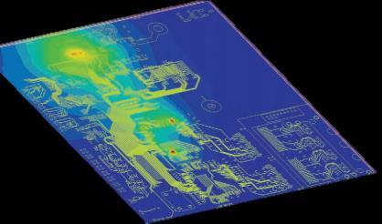


7 Thermal reliability Hot spots Resistive heating of traces Flow pattern ANSYS, Inc. February 2, 2018 ANSYS


8 Structural reliability Trace mapping Exact deformations and stresses ECAD Optimal vibrational behavior Successful passing of the drop test ANSYS, Inc. February 2, 2018 ANSYS


9 ANSYS Solution Geometry Based Reliability Design Multiphysics simulation of printed circuit boards Electro-Thermal Stress Analysis ECAD Design Electrical Reliability Thermal Reliability Power and Signal Integrity Analysis Joule heating Losses Temperature Field Thermal Analysis Temperature Field ANSYS SIwave ANSYS Icepak Mechanical Reliability Stress Analysis ANSYS Mechanical ANSYS, Inc. February 2, 2018 ANSYS


10 ANSYS Electronic Business Unit Driving CPS : Chip-Package-System Convergence Digital RTL PowerArtist CHIP RedHawk PACKAGE Siwave, HFSS,Q3D, Icepak, Mechanical BOARD Siwave, HFSS,Q3D, Icepak, Mechanical DDR RF Analog IPs Totem HDMI FLASH CONNECTOR HFSS, Q3D, Mechanical End-to-End Chip-Package-System Power, Noise, Thermal, EMI, Timing Platform ANSYS, Inc. February 2, 2018 ANSYS

11 ANSYS Technologies for Electronic Systems ANSYS, Inc. February 2, 2018 ANSYS
12 ANSYS SIWAVE FOR SIGNAL AND POWER INTEGRITY ANSYS, Inc. February 2, 2018 ANSYS


13 ANSYS Typical SI/PI Design Flow Electronic Design Environment (Cadence, Mentor, Zuken, Altium...) EM Simulation & Extract Parasitics Database Import Geometry, Stack up, Components Circuit Simulation EM Model Spice S Parameter Verilog-A IBIS 5 IBIS AMI ANSYS, Inc. February 2, 2018 ANSYS


14 DC Power Design Application Example Objective: DC Power Solution All ICs require DC power to operate. It is common for layout engineers to inadvertently cause DC shorts and use too few vias when designing PDNs. ANSYS Solution Use SIwave to predict DC power distribution problems that result in respinning PCBs. This solution finds current bottlenecks, predicts high power losses, and large voltage drops Use bidirectional link with Icepak to determine thermal effects Value of Simulation The simulation of DC power using ANSYS starts with design concepts, includes the influences of manufacturing, and allows detailed evaluation of the power delivery network, signal net routing, connector and via breakouts ANSYS, Inc. February 2, 2018 ANSYS


15 DC Results & Analysis 0.99mΩ 0.96mΩ DC Path Resistance Current Vectors Showing Electron Direction Power & Ground Plane Voltage Drop SIwave Thermal Solves using Icepak ANSYS, Inc. February 2, 2018 ANSYS
16 Timing Analysis Application Example Objective: High Density & High Speed Develop modern electronic devices with greater density of SDRAM (larger RAM) using even-faster speed devices. ANSYS Solution Performs timing analysis that includes signals & PDN Performs fast flight time analysis Performs virtual compliance for memory busses Value of Simulation The simulation of memory, high speed serial links using ANSYS starts with design concepts, includes the influences of manufacturing, and allows detailed evaluation of the power delivery network, signal net routing, connector and via breakouts ANSYS, Inc. February 2, 2018 ANSYS

60 Receiver IC Void B on return")


17 Signal Net Analyzer Impedance & Flight Time Calculations Driver IC U1.(pin)25 Void A on return current path U7.(pin)60 Receiver IC Void B on return current path A digital signal SNA provides: 1. Z o Profile & Delay for all paths of a signal. Zo@ void A Zo@ void B 2. Reflection Noise through transient analysis. Characteristic Impedance Voltage waveform at receiver IC ANSYS, Inc. February 2, 2018 ANSYS


18 Building the Channel Single environment allows extraction of component models such as vias, connectors, and transmission lines as well as concatenating these and other models into a channel schematic S-parameters, eye diagrams, and bit error rate of channel can be simulated Individual components can be optimized and channel results updated quickly TX RX ANSYS, Inc. February 2, 2018 ANSYS

19 Frequency Domain Channel Analysis Simultaneous component- and system-level accuracy allows rapid evaluation of tradeoffs In this example a change from stripline to microstrip improves loss at the expense of crosstalk ANSYS, Inc. February 2, 2018 ANSYS


20 Time Domain Channel Analysis Closed eye at receiver with the stripline topology Open eye at receiver with redesigned microstrip topology. Eye at reference receiver on Stripline topology EH: 62mV ANSYS, Inc. February 2, 2018 ANSYS Eye at reference receiver on improved Microstrip topology
21 AC PDN analysis Application Example Objective: High Density & High Speed Develop modern electronic devices with greater density of SDRAM (larger RAM) using even-faster speed devices. ANSYS Solution Model power delivery networks and noise propagation on PCBs Automates decoupling capacitor selection, placement and optimization Predicts capacitor placement effectiveness by analyzing loop return currents Use CPM models to predict chip performance to complete system-level simulation Value of Simulation Simulation of memory using ANSYS starts with design concepts, includes influences of manufacturing, and allows detailed evaluation of power delivery network, signal net routing, connector and via breakouts ANSYS, Inc. February 2, 2018 ANSYS


22 Power Integrity Analysis Designs of today operate in conjuction with a number of clocks, oscillators, power supplies, and signaling standards. Supplying sufficient power means designing a Power Delivery Network capable of handling any perturbations or irregularities that these complex systems demand. The example below shows voltage for both the time and frequency domain simulation results of a memory interface. A good design will minimize the voltage ripple to ensure that all active devices have a stable and reliable voltage reference. Excessive perturbations in power could cause adverse affects to input and output margins or even couple to other power rails. 873 mv pk-pk due to 200 MHz PRBS ANSYS, Inc. February 2, 2018 ANSYS

 Z (5MHz) V ripple = 5mV = 10mV pk")
23 Supplying Power VRM Transient Simulation Setup Voltage Regulator Module (VRM) is modeled with a series source resistance of 5mΩ for this example. Active Device is modeled as a Current Sink 1A Amplitude: I pk pk = 2A Frequency = 5 MHz Time Delay = 1μs VRM Active Device Example V ripple = I (5MHz) Z (5MHz) V ripple = 5mV = 10mV pk pk ANSYS, Inc. February 2, 2018 ANSYS
24 Supplying Power VRM Frequency Domain Response At DC, Z 11 = 5mΩ which is the VRM series resistance. At f, Z 11 due to the path loop inductance. In this case, a total of 11pH V 0.01n 1p RZ=0.1ohm Z 11 Example V ripple = I (5 MHz) Z (5 MHz) V ripple = 1A 5mΩ V ripple = 5mV = 10mV pk pk ANSYS, Inc. February 2, 2018 ANSYS


25 Early PI Investigations : Auto Select Capacitor Define a VRM Model + PCB using ESR and ESL parameters : Red curves Define an Impedance Mask as Target or Load it Filter Capacitors Vendors, Series, EIA size and run the AUTO ANSYS, Inc. February 2, 2018 ANSYS


26 Simulation of Physical Structures Circuit Simulation vs. Electromagnetic Field Solvers Real, physical designs have many more inductive loops, capacitive planes, and resistive paths which were not depicted in the previous example circuit. In order to account for all of the effects of physical layout and geometry complexities, a field solver such as Siwave or HFSS must be used. In any of the methods shown, loop inductance plays a vital role in determining the frequency of effectiveness. The L-C combination dictates the resonant frequency of adding or changing a capacitor value at a specific location. 1 f resonance = 2π LC Equivalent Series Resistance (ESR) and conductor path resistance affects the quality factor (Q) of the placed component. 1 2πfC Active Device Q = ESR VRM VRM Active Device ANSYS, Inc. February 2, 2018 ANSYS

27 Resonance Simulation Eigenmode analysis identifies location and frequency of natural cavity resonances that exist between planes Scans entire PCB/PKG on all layers If a resonance is excited, Signal Integrity can be compromised : High Z, null in S21, EMI etc. Resonances should be moved away from critical parts and outside operating frequency Reducing Resonance : Resonances always exist but you can reduce their impact by: Changing the decoupling scheme Changing the stackup Changing plane dimensions Adding via stitching Moving discrete parts ANSYS, Inc. February 2, 2018 ANSYS
![SIwave SYZ Analysis Setup to extract [S], Z vs Freq To Perform a circuit extraction or SI analysis, place](/docs-images/88/117483162/images/28-1.jpg "ports in desired location Ports are similar to probes in lab measurements 28 2018 ANSYS, Inc.")
28 SIwave SYZ Analysis Setup to extract [S], Z vs Freq To Perform a circuit extraction or SI analysis, place ports in desired location Ports are similar to probes in lab measurements ANSYS, Inc. February 2, 2018 ANSYS


29 Z11 Power Delivery Network Impedance Full-wave extraction of entire PDN including: Board geometry Passive components : Turn ON or OFF decaps Bare PCB With Capacitors ANSYS, Inc. February 2, 2018 ANSYS


30 PI Advisor: Automated PI Analysis Optimizes Decoupling Capacitors for Power Integrity SIwave AC Solver or PSI AC Solver SIwave AC Solve Time = 15 min 7 sec Frequency Setup 1KHz <= f < 1GHz Genetic Algorithm Setup Optimized for Impedance Optimized for Total Number of Caps Optimized for Capacitor Types Optimized for Price Original solution Total # Caps: 74 Optimized Solution Total # Caps: 18 Capacitor Types = 5 AVX, Samsung, and Kemet 1.7nH 1.0nH.25nH ANSYS, Inc. February 2, 2018 ANSYS


31 PDN Transient Circuit Simulation The final step is to run a transient simulation to look at the Switching Power Noise Load Voltage Swing within 50 mv Target! Time-domain noise specification met ANSYS, Inc. February 2, 2018 ANSYS


 for CLK PRBS7")
, 8b/10b encoding Terminate the pins at the Connector side")
")
32 Example : PCIe3.0 simulation Transient stimulus is applied to critical nets and the Near- and Far-Field response is computed in SIwave using Push Excitation. IBIS model is used for the controller to excite the TX, RX and CLK diff pairs 100MHz clock source (with jitter) for CLK PRBS7 for TX and RX; UI = 1ns (1/1GHz for PCIe3.0), 8b/10b encoding Terminate the pins at the Connector side using Resistors 100ohm differential termination Supply an ideal 1.5V input at the VRM node Connector Side (Termination) Controller Side (Driver) 1.5V supply clk_out Spectral Waveform Power supply lines ANSYS, Inc. February 2, 2018 ANSYS
 E Field @ 100MHz 33 2018 ANSYS, Inc.")
33 EMI/EMC simulation : Near-Field Plots SIwave Near Field analysis is using the results from the transient simulation as current sources to excite the PCB with the true excitations (Push Excitation process) E 100MHz ANSYS, Inc. February 2, 2018 ANSYS


34 Thank you Merci ANSYS, Inc. February 2, 2018 ANSYS
Reliable World Class Insights Your Silicon Valley Partner in Simulation ANSYS Sales, Consulting, Training & Support
 www.ozeninc.com info@ozeninc.com (408) 732 4665 1210 E Arques Ave St 207 Sunnyvale, CA 94085 Reliable World Class Insights Your Silicon Valley Partner in Simulation ANSYS Sales, Consulting, Training &
EMI. Chris Herrick. Applications Engineer
 Fundamentals of EMI Chris Herrick Ansoft Applications Engineer Three Basic Elements of EMC Conduction Coupling process EMI source Emission Space & Field Conductive Capacitive Inductive Radiative Low, Middle
Power integrity is more than decoupling capacitors The Power Integrity Ecosystem. Keysight HSD Seminar Mastering SI & PI Design
 Power integrity is more than decoupling capacitors The Power Integrity Ecosystem Keysight HSD Seminar Mastering SI & PI Design Signal Integrity Power Integrity SI and PI Eco-System Keysight Technologies
Relationship Between Signal Integrity and EMC
 Relationship Between Signal Integrity and EMC Presented by Hasnain Syed Solectron USA, Inc. RTP, North Carolina Email: HasnainSyed@solectron.com 06/05/2007 Hasnain Syed 1 What is Signal Integrity (SI)?
How to anticipate Signal Integrity Issues: Improve my Channel Simulation by using Electromagnetic based model
 How to anticipate Signal Integrity Issues: Improve my Channel Simulation by using Electromagnetic based model HSD Strategic Intent Provide the industry s premier HSD EDA software. Integration of premier
Decoupling capacitor placement
 Decoupling capacitor placement Covered in this topic: Introduction Which locations need decoupling caps? IC decoupling Capacitor lumped model How to maximize the effectiveness of a decoupling cap Parallel
EMC cases study. Antonio Ciccomancini Scogna, CST of America CST COMPUTER SIMULATION TECHNOLOGY
 EMC cases study Antonio Ciccomancini Scogna, CST of America antonio.ciccomancini@cst.com Introduction Legal Compliance with EMC Standards without compliance products can not be released to the market Failure
Power Plane and Decoupling Optimization. Isaac Waldron
 Power Plane and Decoupling Optimization p Isaac Waldron Overview Frequency- and time-domain power distribution system specifications Decoupling design example Bare board Added d capacitors Buried Capacitance
EMI/EMC of Entire Automotive Vehicles and Critical PCB s. Makoto Suzuki Ansoft Corporation
 EMI/EMC of Entire Automotive Vehicles and Critical PCB s Makoto Suzuki Ansoft Corporation WT10_SI EMI/EMC of Entire Automotive Vehicles and Critical PCB s Akira Ohta, Toru Watanabe, Benson Wei Makoto Suzuki
Thank you for downloading one of our ANSYS whitepapers we hope you enjoy it.
 Thank you! Thank you for downloading one of our ANSYS whitepapers we hope you enjoy it. Have questions? Need more information? Please don t hesitate to contact us! We have plenty more where this came from.
Intro. to PDN Planning PCB Stackup Technology Series
 Introduction to Power Distribution Network (PDN) Planning Bill Hargin In-Circuit Design b.hargin@icd.com.au 425-301-4425 Intro. to PDN Planning 1. Intro/Overview 2. Bypass/Decoupling Strategy 3. Plane
Practical Limitations of State of the Art Passive Printed Circuit Board Power Delivery Networks for High Performance Compute Systems
 Practical Limitations of State of the Art Passive Printed Circuit Board Power Delivery Networks for High Performance Compute Systems Presented by Chad Smutzer Mayo Clinic Special Purpose Processor Development
Power Distribution Network Design for Stratix IV GX and Arria II GX FPGAs
 Power Distribution Network Design for Stratix IV GX and Arria II GX FPGAs Transceiver Portfolio Workshops 2009 Question What is Your PDN Design Methodology? Easy Complex Historical Full SPICE simulation
Electromagnetic Simulation of Antennas Installed Inside Vehicles An Automotive EMC Approach Markus Kopp Product Manager, Electronics
 Electromagnetic Simulation of Antennas Installed Inside Vehicles An Automotive EMC Approach Markus Kopp Product Manager, Electronics 1 Automotive Antenna Systems and Automotive EMC Recent technology implementations
Engineering the Power Delivery Network
 C HAPTER 1 Engineering the Power Delivery Network 1.1 What Is the Power Delivery Network (PDN) and Why Should I Care? The power delivery network consists of all the interconnects in the power supply path
High-Performance Electronic Design: Predicting Electromagnetic Interference
 White Paper High-Performance Electronic Design: In designing electronics in today s highly competitive markets, meeting requirements for electromagnetic compatibility (EMC) presents a major risk factor,
EMI Reduction on an Automotive Microcontroller
 EMI Reduction on an Automotive Microcontroller Design Automation Conference, July 26 th -31 st, 2009 Patrice JOUBERT DORIOL 1, Yamarita VILLAVICENCIO 2, Cristiano FORZAN 1, Mario ROTIGNI 1, Giovanni GRAZIOSI
Case Study Package Design & SI/PI analysis
 Caliber Interconnect Solutions Design for perfection Case Study Package Design & SI/PI analysis Caliber Interconnect Solutions (Pvt) Ltd No 6,1 st Street Gandhi Nagar, Kavundampalayam, Coimbatore-30. Tamil
Ensuring Signal and Power Integrity for High-Speed Digital Systems
 Ensuring Signal and Power Integrity for High-Speed Digital Systems An EMC Perspective Christian Schuster Institut für Theoretische Elektrotechnik Technische Universität Hamburg-Harburg (TUHH) Invited Presentation
PDS Impact for DDR Low Cost Design
 PDS Impact for DDR3-1600 Low Cost Design Jack W.C. Lin Sr. AE Manager jackl@cadence.com Aug. g 13 2013 Cadence, OrCAD, Allegro, Sigrity and the Cadence logo are trademarks of Cadence Design Systems, Inc.
System Co-design and optimization for high performance and low power SoC s
 System Co-design and optimization for high performance and low power SoC s Siva S Kothamasu, Texas Instruments Inc, Dallas Snehamay Sinha, Texas Instruments Inc, Dallas Amit Brahme, Texas Instruments India
PCB Routing Guidelines for Signal Integrity and Power Integrity
 PCB Routing Guidelines for Signal Integrity and Power Integrity Presentation by Chris Heard Orange County chapter meeting November 18, 2015 1 Agenda Insertion Loss 101 PCB Design Guidelines For SI Simulation
Electromagnetic Analysis and Verification of Probe Card Performance for First Pass System Success
 San Diego, CA Electromagnetic Analysis and Verification of Probe Card Performance for First Pass System Success Cristian Gozzi Application Engineer Manager Introduction Today in Multi Probe wafer level,
Ansoft Designer with Nexxim. Statistical Eye Capabilities
 Ansoft Designer with Nexxim Statistical Eye Capabilities Problem Statement Load Generic 0.25um M odels Buffer PCIE Connector BYPASS Planar EM S S S TRL TRL TRL TRL TRL TRL Programmable W-Element SI Wave
High Speed Design Issues and Jitter Estimation Techniques. Jai Narayan Tripathi
 High Speed Design Issues and Jitter Estimation Techniques Jai Narayan Tripathi (jainarayan.tripathi@st.com) Outline Part 1 High-speed Design Issues Signal Integrity Power Integrity Jitter Power Delivery
Understanding, measuring, and reducing output noise in DC/DC switching regulators
 Understanding, measuring, and reducing output noise in DC/DC switching regulators Practical tips for output noise reduction Katelyn Wiggenhorn, Applications Engineer, Buck Switching Regulators Robert Blattner,
Signal Integrity Modeling and Simulation for IC/Package Co-Design
 Signal Integrity Modeling and Simulation for IC/Package Co-Design Ching-Chao Huang Optimal Corp. October 24, 2004 Why IC and package co-design? The same IC in different packages may not work Package is
Chapter 16 PCB Layout and Stackup
 Chapter 16 PCB Layout and Stackup Electromagnetic Compatibility Engineering by Henry W. Ott Foreword The PCB represents the physical implementation of the schematic. The proper design and layout of a printed
Automotive PCB SI and PI analysis
 Automotive PCB SI and PI analysis SI PI Analysis Signal Integrity S-Parameter Timing analysis Eye diagram Power Integrity Loop / Partial inductance DC IR-Drop AC PDN Impedance Power Aware SI Signal Integrity
March 6-9, 2016 Hilton Phoenix / Mesa Hotel Mesa, Arizona Archive- Session 4
 Proceedings Archive March 6-9, 2016 Hilton Phoenix / Mesa Hotel Mesa, Arizona Archive- Session 4 2016 BiTS Workshop Image: Stiop / Dollarphotoclub Proceedings Archive Presentation / Copyright Notice The
PDN design and analysis methodology in SI&PI codesign
 PDN design and analysis methodology in SI&PI codesign www.huawei.com Asian IBIS Summit, November 9, 2010, Shenzhen China Luo Zipeng (luozipeng@huawei.com) Liu Shuyao (liushuyao@huawei.com) HUAWEI TECHNOLOGIES
Closing the loop part 1: Why use simulation tools for high speed signal channel design?
 Closing the loop part 1: Why use simulation tools for high speed signal channel design? Riccardo Giacometti Application Engineer Agilent EEsof EDA Page 1 High Speed Digital Design Flow Pre-Layout w/channel
EMC for Printed Circuit Boards
 9 Bracken View, Brocton Stafford, Staffs, UK tel: +44 (0)1785 660 247 fax +44 (0)1785 660 247 email: keith.armstrong@cherryclough.com web: www.cherryclough.com EMC for Printed Circuit Boards Basic and
Effect of Power Noise on Multi-Gigabit Serial Links
 Effect of Power Noise on Multi-Gigabit Serial Links Ken Willis (kwillis@sigrity.com) Kumar Keshavan (ckumar@sigrity.com) Jack Lin (jackwclin@sigrity.com) Tariq Abou-Jeyab (tariqa@sigrity.com) Sigrity Inc.,
DL-150 The Ten Habits of Highly Successful Designers. or Design for Speed: A Designer s Survival Guide to Signal Integrity
 Slide -1 Ten Habits of Highly Successful Board Designers or Design for Speed: A Designer s Survival Guide to Signal Integrity with Dr. Eric Bogatin, Signal Integrity Evangelist, Bogatin Enterprises, www.bethesignal.com
Myoung Joon Choi, Vishram S. Pandit Intel Corp.
 Myoung Joon Choi, Vishram S. Pandit Intel Corp. IBIS Summit at DesignCon 2010 Acknowledgements: Woong Hwan Ryu, Joe Salmon Copyright 2010, Intel Corporation. All rights reserved. Need for SI/PI Co-analysis
Design Considerations for Highly Integrated 3D SiP for Mobile Applications
 Design Considerations for Highly Integrated 3D SiP for Mobile Applications FDIP, CA October 26, 2008 Joungho Kim at KAIST joungho@ee.kaist.ac.kr http://tera.kaist.ac.kr Contents I. Market and future direction
Simulation and Design of Printed Circuit Boards Utilizing Novel Embedded Capacitance Material
 Simulation and Design of Printed Circuit Boards Utilizing Novel Embedded Capacitance Material April 28, 2010 Yu Xuequan, Yanhang, Zhang Gezi, Wang Haisan Huawei Technologies CO., LTD. Shanghai, China Tony_yu@huawei.com
The Inductance Loop Power Distribution in the Semiconductor Test Interface. Jason Mroczkowski Multitest
 The Inductance Loop Power Distribution in the Semiconductor Test Interface Jason Mroczkowski Multitest j.mroczkowski@multitest.com Silicon Valley Test Conference 2010 1 Agenda Introduction to Power Delivery
A Resonance-Free Power Delivery System Design Methodology applying 3D Optimized Extended Adaptive Voltage Positioning.
 A Resonance-Free Power Delivery System Design Methodology applying 3D Optimized Extended Adaptive Voltage Positioning Tao Xu Brad Brim Agenda Adaptive voltage positioning (AVP) Extended adaptive voltage
Decoupling capacitor uses and selection
 Decoupling capacitor uses and selection Proper Decoupling Poor Decoupling Introduction Covered in this topic: 3 different uses of decoupling capacitors Why we need decoupling capacitors Power supply rail
Signal Integrity Design of TSV-Based 3D IC
 Signal Integrity Design of TSV-Based 3D IC October 24, 21 Joungho Kim at KAIST joungho@ee.kaist.ac.kr http://tera.kaist.ac.kr 1 Contents 1) Driving Forces of TSV based 3D IC 2) Signal Integrity Issues
PI6C557-03AQ. PCIe 2.0 Clock Generator with 2 HCSL Outputs for Automotive Applications. Description. Features. Pin Configuration (16-Pin TSSOP)
") PCIe.0 Clock Generator with HCSL Outputs for Automotive Applications Features ÎÎPCIe.0 compliant à à Phase jitter -.1ps RMS (typ) ÎÎLVDS compatible outputs ÎÎSupply voltage of 3.3V ±10% ÎÎ5MHz crystal
PCIe.0 Clock Generator with HCSL Outputs for Automotive Applications Features ÎÎPCIe.0 compliant à à Phase jitter -.1ps RMS (typ) ÎÎLVDS compatible outputs ÎÎSupply voltage of 3.3V ±10% ÎÎ5MHz crystal
DesignCon Effect of Power Plane Inductance on Power Delivery Networks. Shirin Farrahi, Cadence Design Systems
 DesignCon 2019 Effect of Power Plane Inductance on Power Delivery Networks Shirin Farrahi, Cadence Design Systems shirinf@cadence.com, 978-262-6008 Ethan Koether, Oracle Corp ethan.koether@oracle.com Mehdi
DL-150 The Ten Habits of Highly Successful Designers. or Design for Speed: A Designer s Survival Guide to Signal Integrity
 Slide -1 Ten Habits of Highly Successful Board Designers or Design for Speed: A Designer s Survival Guide to Signal Integrity with Dr. Eric Bogatin, Signal Integrity Evangelist, Bogatin Enterprises, www.bethesignal.com
EMI Modeling of a 32-bit Microcontroller in Wait Mode
 EMI Modeling of a 32-bit Microcontroller in Wait Mode Jean-Pierre Leca 1,2, Nicolas Froidevaux 1, Henri Braquet 2, Gilles Jacquemod 2 1 STMicroelectronics, 2 LEAT, UMR CNRS-UNS 6071 BMAS 2010 San Jose,
A Novel Embedded Common-mode Filter for above GHz differential signals based on Metamaterial concept. Tzong-Lin Wu
 c //3 A Novel Embedded Common-mode Filter for above GHz differential signals based on Metamaterial concept Tzong-Lin Wu Professor Graduate Institute of Communication Engineering, National Taiwan University,
W2360EP/ET SIPro Signal Integrity EM Analysis W2359EP/ET PIPro Power Integrity EM Analysis
 Keysight Technologies Advanced Design System (ADS) W2360EP/ET SIPro Signal Integrity EM Analysis W2359EP/ET PIPro Power Integrity EM Analysis Data Sheet Composite EM technology delivers high-accuracy and
Validation Report Comparison of Eye Patterns Generated By Synopsys HSPICE and the Agilent PLTS
 Comparison of Eye Patterns Generated By Synopsys HSPICE and the Agilent PLTS Using: Final Inch Test/Eval Kit, Differential Pair - No Grounds Configuration, QTE-DP/QSE-DP, 5mm Stack Height (P/N FIK-QxE-04-01)
Effective Routing of Multiple Loads
 feature column BEYOND DESIGN Effective Routing of Multiple Loads by Barry Olney In a previous Beyond Design, Impedance Matching: Terminations, I discussed various termination strategies and concluded that
PCI-EXPRESS CLOCK SOURCE. Features
 DATASHEET ICS557-01 Description The ICS557-01 is a clock chip designed for use in PCI-Express Cards as a clock source. It provides a pair of differential outputs at 100 MHz in a small 8-pin SOIC package.
TIE Plus. The step towards interconnect simulation technology
 Bitte decken Sie die schraffierte Fläche mit einem Bild ab. Please cover the shaded area with a picture. (24,4 x 11,0 cm) TIE Plus. The step towards interconnect simulation technology Catalin Negrea, Ph.
Taking the Mystery out of Signal Integrity
 Slide - 1 Jan 2002 Taking the Mystery out of Signal Integrity Dr. Eric Bogatin, CTO, GigaTest Labs Signal Integrity Engineering and Training 134 S. Wolfe Rd Sunnyvale, CA 94086 408-524-2700 www.gigatest.com
The Challenges of Differential Bus Design
 The Challenges of Differential Bus Design February 20, 2002 presented by: Arthur Fraser TechKnowledge Page 1 Introduction Background Historically, differential interconnects were often twisted wire pairs
BASIS OF ELECTROMAGNETIC COMPATIBILITY OF INTEGRATED CIRCUIT Chapter VI - MODELLING PCB INTERCONNECTS Corrections of exercises
 BASIS OF ELECTROMAGNETIC COMPATIBILITY OF INTEGRATED CIRCUIT Chapter VI - MODELLING PCB INTERCONNECTS Corrections of exercises I. EXERCISE NO 1 - Spot the PCB design errors Spot the six design errors in
Introduction to EMI/EMC Challenges and Their Solution
 Introduction to EMI/EMC Challenges and Their Solution Dr. Hany Fahmy HSD Application Expert Agilent Technologies Davy Pissort, K.U. Leuven Charles Jackson, Nvidia Charlie Shu, Nvidia Chen Wang, Nvidia
Innovations in EDA Webcast Series
 Welcome Innovations in EDA Webcast Series August 2, 2012 Jack Sifri MMIC Design Flow Specialist IC, Laminate, Package Multi-Technology PA Module Design Methodology Realizing the Multi-Technology Vision
Development and Validation of a Microcontroller Model for EMC
 Development and Validation of a Microcontroller Model for EMC Shaohua Li (1), Hemant Bishnoi (1), Jason Whiles (2), Pius Ng (3), Haixiao Weng (2), David Pommerenke (1), and Daryl Beetner (1) (1) EMC lab,
ICS PCI-EXPRESS CLOCK SOURCE. Description. Features. Block Diagram DATASHEET
 DATASHEET ICS557-0 Description The ICS557-0 is a clock chip designed for use in PCI-Express Cards as a clock source. It provides a pair of differential outputs at 00 MHz in a small 8-pin SOIC package.
The amout, type and position definition and optimization of decoupling capacitors which depend on the resonance hot spot position,
 Resonance Simulation in PI Design Xiao Dan Nokia Abstract PCB power-ground resonance theory is introduced and relationship between Z simulated parameter and resonance frequency is discussed based on the
Optimization of Wafer Level Test Hardware using Signal Integrity Simulation
 June 7-10, 2009 San Diego, CA Optimization of Wafer Level Test Hardware using Signal Integrity Simulation Jason Mroczkowski Ryan Satrom Agenda Industry Drivers Wafer Scale Test Interface Simulation Simulation
Demystifying Vias in High-Speed PCB Design
 Demystifying Vias in High-Speed PCB Design Keysight HSD Seminar Mastering SI & PI Design db(s21) E H What is Via? Vertical Interconnect Access (VIA) An electrical connection between layers to pass a signal
Plane Crazy, Part 2 BEYOND DESIGN. by Barry Olney
 by Barry Olney column BEYOND DESIGN Plane Crazy, Part 2 In my recent four-part series on stackup planning, I described the best configurations for various stackup requirements. But I did not have the opportunity
Response Surface Channel Modeling Designer SI & DesignXplorer
 Response Surface Channel Modeling Designer SI & DesignXplorer 1 ANSYS, Inc. September 14, Outline Product Introductions Designer SI DesignXplorer Intro to DOE & Response Surface Modeling Response Surfaces
Printed circuit board power distribution network modeling, analysis and design, and, statistical crosstalk analysis for high speed digital links
 Scholars' Mine Doctoral Dissertations Student Research & Creative Works Spring 2015 Printed circuit board power distribution network modeling, analysis and design, and, statistical crosstalk analysis for
DDR4 memory interface: Solving PCB design challenges
 DDR4 memory interface: Solving PCB design challenges Chang Fei Yee - July 23, 2014 Introduction DDR SDRAM technology has reached its 4th generation. The DDR4 SDRAM interface achieves a maximum data rate
Research in Support of the Die / Package Interface
 Research in Support of the Die / Package Interface Introduction As the microelectronics industry continues to scale down CMOS in accordance with Moore s Law and the ITRS roadmap, the minimum feature size
High Speed Digital Systems Require Advanced Probing Techniques for Logic Analyzer Debug
 JEDEX 2003 Memory Futures Track 2 March 25, 2003 High Speed Digital Systems Require Advanced Probing Techniques for Logic Analyzer Debug Author/Presenter: Brock LaMeres Hardware Design Engineer Objective
Learning the Curve BEYOND DESIGN. by Barry Olney
 by Barry Olney coulmn BEYOND DESIGN Learning the Curve Currently, power integrity is just entering the mainstream market phase of the technology adoption life cycle. The early market is dominated by innovators
High Speed Digital Systems Require Advanced Probing Techniques for Logic Analyzer Debug
 JEDEX 2003 Memory Futures (Track 2) High Speed Digital Systems Require Advanced Probing Techniques for Logic Analyzer Debug Brock J. LaMeres Agilent Technologies Abstract Digital systems are turning out
Signal Integrity, Part 1 of 3
 by Barry Olney feature column BEYOND DESIGN Signal Integrity, Part 1 of 3 As system performance increases, the PCB designer s challenges become more complex. The impact of lower core voltages, high frequencies
VLSI is scaling faster than number of interface pins
 High Speed Digital Signals Why Study High Speed Digital Signals Speeds of processors and signaling Doubled with last few years Already at 1-3 GHz microprocessors Early stages of terahertz Higher speeds
Design Fundamentals by A. Ciccomancini Scogna, PhD Suppression of Simultaneous Switching Noise in Power and Ground Plane Pairs
 Design Fundamentals by A. Ciccomancini Scogna, PhD Suppression of Simultaneous Switching Noise in Power and Ground Plane Pairs Photographer: Janpietruszka Agency: Dreamstime.com 36 Conformity JUNE 2007
Split Planes in Multilayer PCBs
 by Barry Olney coulmn BEYOND DESIGN Split Planes in Multilayer PCBs Creating split planes or isolated islands in the copper planes of multilayer PCBs at first seems like a good idea. Today s high-speed
Ansys Designer RF Training Lecture 3: Nexxim Circuit Analysis for RF
 Ansys Designer RF Solutions for RF/Microwave Component and System Design 7. 0 Release Ansys Designer RF Training Lecture 3: Nexxim Circuit Analysis for RF Designer Overview Ansoft Designer Advanced Design
Design for Guaranteed EMC Compliance
 Clemson Vehicular Electronics Laboratory Reliable Automotive Electronics Automotive EMC Workshop April 29, 2013 Design for Guaranteed EMC Compliance Todd Hubing Clemson University EMC Requirements and
Texas Instruments DisplayPort Design Guide
 Texas Instruments DisplayPort Design Guide April 2009 1 High Speed Interface Applications Introduction This application note presents design guidelines, helping users of Texas Instruments DisplayPort devices
Device-Specific Power Delivery Network (PDN) Tool User Guide
 Tool User Guide") Device-Specific Power Delivery Network (PDN) Tool User Guide Device-Specific Power Delivery Network (PDN) Tool User Guide 101 Innovation Drive San Jose, CA 95134 www.altera.com UG-01134-1.1 Subscribe 2014
Device-Specific Power Delivery Network (PDN) Tool User Guide Device-Specific Power Delivery Network (PDN) Tool User Guide 101 Innovation Drive San Jose, CA 95134 www.altera.com UG-01134-1.1 Subscribe 2014
PI6C557-03B. PCIe 3.0 Clock Generator with 2 HCSL Outputs. Features. Description. Pin Configuration (16-Pin TSSOP) Block Diagram
 Block Diagram") Features ÎÎPCIe 3.0 compliant à à PCIe 3.0 Phase jitter - 0.45ps RMS (High Freq. Typ.) ÎÎLVDS compatible outputs ÎÎSupply voltage of 3.3V ±10% ÎÎ5MHz crystal or clock input frequency ÎÎHCSL outputs, 0.8V
Features ÎÎPCIe 3.0 compliant à à PCIe 3.0 Phase jitter - 0.45ps RMS (High Freq. Typ.) ÎÎLVDS compatible outputs ÎÎSupply voltage of 3.3V ±10% ÎÎ5MHz crystal or clock input frequency ÎÎHCSL outputs, 0.8V
CIRCUITS. Raj Nair Donald Bennett PRENTICE HALL
 POWER INTEGRITY ANALYSIS AND MANAGEMENT I CIRCUITS Raj Nair Donald Bennett PRENTICE HALL Upper Saddle River, NJ Boston Indianapolis San Francisco New York Toronto Montreal London Munich Paris Madrid Capetown
Ansoft Electronic Design Automation
 Ansoft Electronic Design Automation Desmond Tan Technical Manager ANSOFT, LLC. 28 Ansoft, LLC All rights reserved. Ansoft, LLC Proprietary Ansoft Products And Technology Ansoft provides state-of-the-art
Optimizing Design of a Probe Card using a Field Solver
 Optimizing Design of a Probe Card using a Field Solver Rey Rincon, r-rincon@ti.com Texas Instruments 13020 Floyd Rd MS 3616 Dallas, TX. 75243 972-917-4303 Eric Bogatin, bogatin@ansoft.com Bill Beale, beale@ansoft.com
Passive Components around ADAS Applications By Ron Demcko, AVX Fellow, AVX Corporation
 Passive Components around ADAS Applications By Ron Demcko, AVX Fellow, AVX Corporation The importance of high reliability - high performance electronics is accelerating as Advanced Driver Assistance Systems
Bridging the Measurement and Simulation Gap Sarah Boen Marketing Manager Tektronix
 Bridging the Measurement and Simulation Gap Sarah Boen Marketing Manager Tektronix 1 Agenda Synergy between simulation and lab based measurements IBIS-AMI overview Simulation and measurement correlation
DC/DC Converter. Conducted Emission. CST COMPUTER SIMULATION TECHNOLOGY
 DC/DC Converter Conducted Emission Introduction 3D Model EDA Layout Simulation Modifications N GOALS MET? Y In modern electronic applications a majority of devices utilizes switched AC/DC or DC/DC converters
DEPARTMENT FOR CONTINUING EDUCATION
 DEPARTMENT FOR CONTINUING EDUCATION Reduce EMI Emissions for FREE! by Bruce Archambeault, Ph.D. (reprinted with permission from Bruce Archambeault) Bruce Archambeault presents two courses during the University
2.5D & 3D Package Signal Integrity A Paradigm Shift
 2.5D & 3D Package Signal Integrity A Paradigm Shift Nozad Karim Technology & Platform Development November, 2011 Enabling a Microelectronic World Content Traditional package signal integrity vs. 2.5D/3D
Characterization of Alternate Power Distribution Methods for 3D Integration
 Characterization of Alternate Power Distribution Methods for 3D Integration David C. Zhang, Madhavan Swaminathan, David Keezer and Satyanarayana Telikepalli School of Electrical and Computer Engineering,
Chip Package - PC Board Co-Design: Applying a Chip Power Model in System Power Integrity Analysis
 Chip Package - PC Board Co-Design: Applying a Chip Power Model in System Power Integrity Analysis Authors: Rick Brooks, Cisco, ricbrook@cisco.com Jane Lim, Cisco, honglim@cisco.com Udupi Harisharan, Cisco,
Experience at INFN Padova on constrained PCB design Roberto Isocrate INFN-Padova
 Experience at INFN Padova on constrained PCB design Roberto Isocrate INFN-Padova Experience at INFN Padova on constrained design 1. Why do we need Signal Integrity (SI) analysis (and constrained design)?
Broadband Methodology for Power Distribution System Analysis of Chip, Package and Board for High Speed IO Design
 DesignCon 2009 Broadband Methodology for Power Distribution System Analysis of Chip, Package and Board for High Speed IO Design Hsing-Chou Hsu, VIA Technologies jimmyhsu@via.com.tw Jack Lin, Sigrity Inc.
Microcircuit Electrical Issues
 Microcircuit Electrical Issues Distortion The frequency at which transmitted power has dropped to 50 percent of the injected power is called the "3 db" point and is used to define the bandwidth of the
Electromagnetic Analysis of AC Coupling Capacitor Mounting Structures
 Simbeor Application Note #2008_02, April 2008 2008 Simberian Inc. Electromagnetic Analysis of AC Coupling Capacitor Mounting Structures Simberian, Inc. www.simberian.com Simbeor : Easy-to-Use, Efficient
Technology in Balance
 Technology in Balance A G1 G2 B Basic Structure Comparison Regular capacitors have two plates or electrodes surrounded by a dielectric material. There is capacitance between the two conductive plates within
Signal Integrity Tips and Techniques Using TDR, VNA and Modeling. Russ Kramer O.J. Danzy
 Signal Integrity Tips and Techniques Using TDR, VNA and Modeling Russ Kramer O.J. Danzy Simulation What is the Signal Integrity Challenge? Tx Rx Channel Asfiakhan Dreamstime.com - 3d People Communication
Understanding and Optimizing Electromagnetic Compatibility in Switchmode Power Supplies
 Understanding and Optimizing Electromagnetic Compatibility in Switchmode Power Supplies 1 Definitions EMI = Electro Magnetic Interference EMC = Electro Magnetic Compatibility (No EMI) Three Components
Introduction to Board Level Simulation and the PCB Design Process
 BEYOND DESIGN C O L U M N Introduction to Board Level Simulation and the PCB Design Process by Barry Olney IN-CIRCUIT DESIGN PTY LTD AUSTRALIA SUMMARY Board-level simulation reduces costs by identifying
Measuring Hot TDR and Eye Diagrams with an Vector Network Analyzer?
 Measuring Hot TDR and Eye Diagrams with an Vector Network Analyzer? Gustaaf Sutorius Application Engineer Agilent Technologies gustaaf_sutorius@agilent.com Page 1 #TDR fit in Typical Digital Development
PI6C PCI Express Clock. Product Features. Description. Block Diagram. Pin Configuration
 Product Features ÎÎLVDS compatible outputs ÎÎSupply voltage of 3.3V ±10% ÎÎ5MHz input frequency ÎÎHCSL outputs, 0.7V Current mode differential pair ÎÎJitter 60ps cycle-to-cycle (typ) ÎÎSpread of ±0.5%,
Si-Interposer Collaboration in IC/PKG/SI. Eric Chen
 Si-Interposer Collaboration in IC/PKG/SI Eric Chen 4/Jul/2014 Design Overview U-bump Logic IC Mem IC C4 bump Logic IC Silicon/Organic substrate Interposer Mem IC CAP Package substrate Solder Ball VRM BGA