Experience at INFN Padova on constrained PCB design Roberto Isocrate INFN-Padova
|
|
|
- Kory Campbell
- 6 years ago
- Views:
Transcription
1 Experience at INFN Padova on constrained PCB design Roberto Isocrate INFN-Padova
2 Experience at INFN Padova on constrained design 1. Why do we need Signal Integrity (SI) analysis (and constrained design)? 2. Design approach and Cadence tools 3. Agata GTS card description 4. Comparison between simulations and reality 5. Allegro SI 630 MGH short description 6. MGH simulations compared to reality


3 Why do we need SI and PI analysis? Die size decreasing Technology evolution Rise time becoming more rapid (bandwidth increasing) Lower power-supply voltage More current Critical length decreases Traces must be treated as transmission lines Less noise margin Impedance of power planes depends strongly on frequency
4 Technology Trend Decreasing Rise Time And Supply Voltage Increasing Number of Constrained Nets and Supply Current Technology
5 How Constrained Design Help designers? Logic Design Layout Allegro Design Entry HDL SI 610 Allegro PCB SI board Electrical Engineers SI Engineers Layout Designers ECSets
6 Typical design approach Logical Design System/Board Partitioning Up Front Concurrent Electrical/Physical Design Mechanical Design Pre- Layout Design Constrain Sets Constrain Driven PCB Layout And Verification Pre- Proto Sign-Off Prototype Fabrication and assembly Physical Hardware Verification Pre- Production Design Production Hardware
7 AGATA GTS Mezzanine card: short description Clock Generator isfp Transceiver Delay lines Jitter attenuator isfp Transceiver 2V5 Reg FLASH (boot) Mem Xilinx Virtex2Pro FPGA isfp Transceiver 1V5 Reg SDRAM SDRAM Memory Memory Mictor Mictor connectors connectors J1 J1 J2 J2 isfp Transceiver 10/100 Enet PHY


8 Brief description of Global Clock and Trigger distribution


9 AGATA GTS Mezzanine card short description isfp transceivers High speed cross-switch Clock generator FLASH Temp. sensor Tyco Mictor connectors Clock smoother FPGA Delay lines SDRAM

 Luciano")


10 AGATA Global Trigger and Clock Distribution System The Team Marco Bellato (project leader) Luciano Berti Damiano Bortolato Roberto Isocrate Gabriele Rampazzo More info about AGATA AGATA web page


11 Cadence Allegro SI design approach Define specifications Simulation topologies Schematic entry Board debug Electrical and mechanical constrains, stackup, Post layout constrain evaluation Post layout SI verifications Board routing

12 Define specifications and Simulation Topologies


13 Models, Curves, Topologies


14 IBIS model sources The web : Google search Cadence libraries The supplier 3rd party custom
15 If you don t find a model Build it! Key ingredients: Pin List, I/O cell V-I curves, dv/dt, threshold voltages, etc. Embellishments: V-T curves, etc. Check run through parsers: IBIS: ibischk3 Cadence: ibis2signoise I/O cell source: Simulate from SPICE --> not likely & what s the point? Borrow something similar ********************************************************************* [IBIS Ver] 3.1 [File Name] rgl_1638.ibs [File Rev] 2.0 [Source] Borrowed and modified by RGL from a similar part HDMP_1636 also supplied by Agilent with the warning that the IO cells are somewhat different [Date] 6_12_00 ********************************************************************* (C) COPYRIGHT Com Corporation ********************************************************************* [Component] RGL_HDMP_1638 [Manufacturer] HP [Package] variable typ min max R_pkg.06ohms NA NA L_pkg 6.0nH NA NA C_pkg.5pF NA NA [Pin] signal_name model_name R_pin L_pin C_pin 1 GND_TXHS GND n.3p 2 TX0 Z530678_IN n.29p 3 TX1 Z530678_IN n.28p 4 TX2 Z530678_IN n.27p 5 TX3 Z530678_IN n.26p 6 TX4 Z530678_IN n.25p 7 TX5 Z530678_IN n.25p 8 TX6 Z530678_IN n.24p 9 TX7 Z530678_IN n.24p 10 TX8 Z530678_IN n.25p 11 TX9 Z530678_IN n.25p 12 NC NC 13 RXSEL Z530678_IN n.27p
16 Why IBIS? Advantages -Fast -Easy -Doesn t reveal proprietary information -Complete chip definition -Pin out - Cell Usage - AC and DC Specifications Disadvantages -IBIS model quality is generally poor -Accuracy can be an issue - Practical Issues and Limitations - Connectors/Package models - Different results from different simulators (portability) -IBIS committee slow to respond Advantages -Industry Standard - Berkley SPICE is Free - HSPICE has widespread acceptance -Accurate - Transistor levels models - Connectors, lossy transmission lines - if you can build it, you can model it Why SPICE? Disadvantages -Performance can be slow -Inconsistent net list formats and cryptic spice syntax

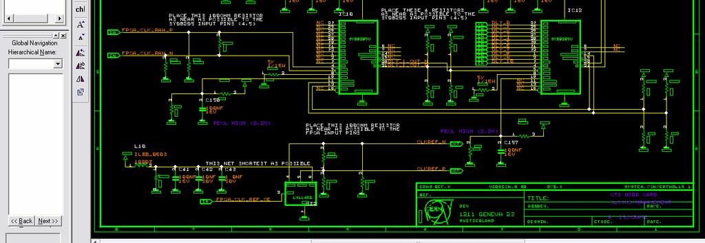
17 Schematic design entry


18 Define electrical constraints, stackup, mechanical constraints,

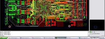
19 Board layout: place
20 and route

21 Post layout constraints evaluation


22 Example of propagation-delay equalization

23 Post layout SI verifications

24 Board debugging

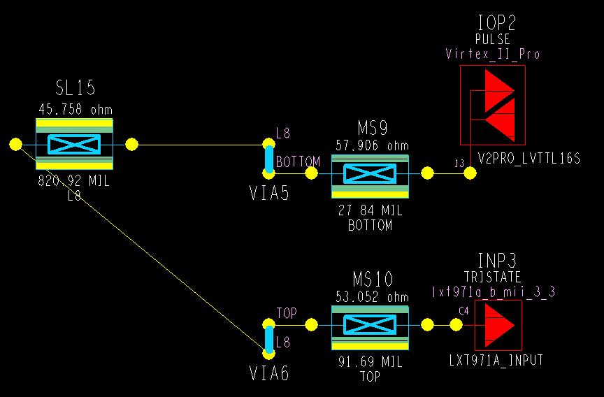
25 Post layout topology extraction: examples #1
26 Post layout topology extraction: example #1

27 Post layout topology extraction: example #2

28 Post layout topology extraction: example #2

29 Post layout topology extraction: example #3

30 Post layout topology extraction: example #3


31 Post layout topology extraction: example #4


32 MGH design features System Analysis: Time domain simulations Loss Budgeting: S-parameters simulations High Capacity: Channel Analysis


33 Allegro PCB SI 630 Multi-GHz Technology There are two ways to simulate Tlsim Hspice


34 Wrap hspice model in dml 4 5 stimuli enable Need to map active device nodes to those shown Additional nodes can be used, these are simply the nodes the GUI interacts with 2 inputs 4 power pins Node 2 (and diff node 8) connect to interconnect for inputs, outputs, and IOs At the text level NOT TRIVIAL!
35 Hspice Wrapping Process Understand model to wrap Nodes, voltages, frequencies, etc Identify any related files (called, included or encrypted) Understand template Position of model subckt AND header info Header: model name, type, voltage, ramp, language, number of terminals Normal = 7-terminal, Differential = 8-terminal Worst case = BBox, (decision flow in Hspice Guide App. A) Paste model into template Fix header attributes Adapt nodes in model to nodes in template Test in simple circuit with SigXp calling Hspice and debug Find problems by searching for error in waveforms.lis Get more help at if needed

36 Post layout topology extraction of Gigabit lanes


37 Define stimulus


38 Run simulation It takes time! ~50minutes on 2 GHz Intel!!)


39 Gigabit lane simulation results


40 Gigabit lane simulation vs. measurements


41 MGH Analysis Loss budget Loss budget -13.8dB

42 MGH Analysis S-parameters Loss budget -13.8dB

43 Channel analysis Interconnect Storage Potential


44 It is very easy to introduce impedance discontinuities! Follow the rules!! Vias clearance! High speed differential vias Equalize the length difference between N and P signals Avoid stubs (if possible)


45 MGH analysis example how impedance discontinuities degrade the SI
46 Conclusions Constrained design offers an integrated high-speed design and analysis solution. Reading and writing to the same database avoid possible translation issues. SI analysis enables you to solve issues early in the design process. Due to the miniaturizations of components it is very complex to fix errors on prototypes Improved chances of first time success
Relationship Between Signal Integrity and EMC
 Relationship Between Signal Integrity and EMC Presented by Hasnain Syed Solectron USA, Inc. RTP, North Carolina Email: HasnainSyed@solectron.com 06/05/2007 Hasnain Syed 1 What is Signal Integrity (SI)?
IBIS Models: Background and Usage
 Technical Brief Introduction For better understanding of the signal integrity on printed circuit boards (PCBs), hardware designers often need to simulate the design with I/O characteristic models. The
Si-Interposer Collaboration in IC/PKG/SI. Eric Chen
 Si-Interposer Collaboration in IC/PKG/SI Eric Chen 4/Jul/2014 Design Overview U-bump Logic IC Mem IC C4 bump Logic IC Silicon/Organic substrate Interposer Mem IC CAP Package substrate Solder Ball VRM BGA
How to anticipate Signal Integrity Issues: Improve my Channel Simulation by using Electromagnetic based model
 How to anticipate Signal Integrity Issues: Improve my Channel Simulation by using Electromagnetic based model HSD Strategic Intent Provide the industry s premier HSD EDA software. Integration of premier
Taking the Mystery out of Signal Integrity
 Slide - 1 Jan 2002 Taking the Mystery out of Signal Integrity Dr. Eric Bogatin, CTO, GigaTest Labs Signal Integrity Engineering and Training 134 S. Wolfe Rd Sunnyvale, CA 94086 408-524-2700 www.gigatest.com
IBIS Data for CML,PECL and LVDS Interface Circuits
 Application Note: HFAN-06.2 Rev.1; 04/08 IBIS Data for CML,PECL and LVDS Interface Circuits AVAILABLE IBIS Data for CML,PECL and LVDS Interface Circuits 1 Introduction The integrated circuits found in
Digital Systems Design
 Digital Systems Design Digital Systems Design and Test Dr. D. J. Jackson Lecture 1-1 Introduction Traditional digital design Manual process of designing and capturing circuits Schematic entry System-level
EMC Simulation Signal Integrity Simulation in Automotive Design
 Bitte decken Sie die schraffierte Fläche mit einem Bild ab. Please cover the shaded area with a picture. (24,4 x 11,0 cm) EMC Simulation Signal Integrity Simulation in Automotive Design Stefanie Schatt
DP Array DPAM/DPAF Final Inch Designs in Serial ATA Generation 1 Applications 10mm Stack Height. REVISION DATE: January 11, 2005
 Application Note DP Array DPAM/DPAF Final Inch Designs in Serial ATA Generation 1 Applications 10mm Stack Height REVISION DATE: January 11, 2005 Copyrights and Trademarks Copyright 2005 Samtec, Inc. Developed
Myoung Joon Choi, Vishram S. Pandit Intel Corp.
 Myoung Joon Choi, Vishram S. Pandit Intel Corp. IBIS Summit at DesignCon 2010 Acknowledgements: Woong Hwan Ryu, Joe Salmon Copyright 2010, Intel Corporation. All rights reserved. Need for SI/PI Co-analysis
Impedance Matching: Terminations
 by Barry Olney IN-CIRCUIT DESIGN PTY LTD AUSTRALIA column BEYOND DESIGN Impedance Matching: Terminations The impedance of the trace is extremely important, as any mismatch along the transmission path will
IBIS Simulation for High-Speed Memory Interface Board Suggestions : How to use IBIS model correctly
 IBIS Simulation for High-Speed Memory Interface Board Suggestions : How to use IBIS model correctly Masaki Kirinaka, Akiko Tsukada FUJITSU INTERCONNECT TECHNOLOGIES LIMITED Asian IBIS Summit Tokyo, JAPAN
A Simulation Study of Simultaneous Switching Noise
 A Simulation Study of Simultaneous Switching Noise Chi-Te Chen 1, Jin Zhao 2, Qinglun Chen 1 1 Intel Corporation Network Communication Group, LOC4/19, 9750 Goethe Road, Sacramento, CA 95827 Tel: 916-854-1178,
ANSYS CPS SOLUTION FOR SIGNAL AND POWER INTEGRITY
 ANSYS CPS SOLUTION FOR SIGNAL AND POWER INTEGRITY Rémy FERNANDES Lead Application Engineer ANSYS 1 2018 ANSYS, Inc. February 2, 2018 ANSYS ANSYS - Engineering simulation software leader Our industry reach
User2User The 2007 Mentor Graphics International User Conference
 7/2/2007 1 Designing High Speed Printed Circuit Boards Using DxDesigner and Expedition Robert Navarro Jet Propulsion Laboratory, California Institute of Technology. User2User The 2007 Mentor Graphics International
RiseUp RU8-DP-DV Series 19mm Stack Height Final Inch Designs in Serial ATA Generation 1 Applications. Revision Date: March 18, 2005
 RiseUp RU8-DP-DV Series 19mm Stack Height Final Inch Designs in Serial ATA Generation 1 Applications Revision Date: March 18, 2005 Copyrights and Trademarks Copyright 2005 Samtec, Inc. Developed in conjunction
Q2 QMS-DP/QFS-DP Series 11 mm Stack Height Final Inch Designs in Serial ATA Generation 1 Applications. Revision Date: February 22, 2005
 Q2 QMS-DP/QFS-DP Series 11 mm Stack Height Final Inch Designs in Serial ATA Generation 1 Applications Revision Date: February 22, 2005 Copyrights and Trademarks Copyright 2005 Samtec, Inc. Developed in
Automotive PCB SI and PI analysis
 Automotive PCB SI and PI analysis SI PI Analysis Signal Integrity S-Parameter Timing analysis Eye diagram Power Integrity Loop / Partial inductance DC IR-Drop AC PDN Impedance Power Aware SI Signal Integrity
QPairs QTE-DP/QSE-DP Final Inch Designs in Serial ATA Generation 1 Applications 5mm Stack Height. REVISION DATE: January 12, 2005
 Application Note QPairs QTE-DP/QSE-DP Final Inch Designs in Serial ATA Generation 1 Applications 5mm Stack Height REVISION DATE: January 12, 2005 Copyrights and Trademarks Copyright 2005 Samtec, Inc. Developed
IBIS OPEN FORUM I/O BUFFER MODELING COOKBOOK Version 4.0 Revision 0.8 Prepared By: The IBIS Open Forum
 Senior Editor: Michael Mirmak Intel Corp. IBIS OPEN FORUM I/O BUFFER MODELING COOKBOOK Version 4.0 Revision 0.8 Prepared By: The IBIS Open Forum Contributors: John Angulo, Mentor Graphics Corp. Ian Dodd,
Caliber Interconnect Solutions
 Caliber Interconnect Solutions Design for perfection CASE STUDY DBFSP card and Optical card Transceivers Channels (through Backplane) Pre-Layout SI Report Caliber Interconnect Solutions (Pvt) Ltd No 6,1
IBIS OPEN FORUM I/O BUFFER MODELING COOKBOOK Version 4.0 Revision 0.95 Prepared By: The IBIS Open Forum
 IBIS OPEN FORUM I/O BUFFER MODELING COOKBOOK Version 4.0 Revision 0.95 Prepared By: The IBIS Open Forum Deleted: 9AM1 Senior Editor: Michael Mirmak Intel Corp. Contributors: John Angulo, Mentor Graphics
Signal Integrity Modeling and Simulation for IC/Package Co-Design
 Signal Integrity Modeling and Simulation for IC/Package Co-Design Ching-Chao Huang Optimal Corp. October 24, 2004 Why IC and package co-design? The same IC in different packages may not work Package is
Compact Camera Port 2 SubLVDS with 7 Series FPGAs High-Range I/O Author: Brandon Day
 Application Note: 7 Series FPGAs XAPP582 (v1.0) January 31, 2013 Compact Camera Port 2 SubLVDS with 7 Series FPGAs High-Range I/O Author: Brandon Day Summary The Compact Camera Port 2 (CCP2) protocol is
High Speed Digital Systems Require Advanced Probing Techniques for Logic Analyzer Debug
 JEDEX 2003 Memory Futures Track 2 March 25, 2003 High Speed Digital Systems Require Advanced Probing Techniques for Logic Analyzer Debug Author/Presenter: Brock LaMeres Hardware Design Engineer Objective
DesignCon 2003 High-Performance System Design Conference (HP3-5)
") DesignCon 2003 High-Performance System Design Conference (HP3-5) Logic Analyzer Probing Techniques for High-Speed Digital Systems Author/Presenter: Brock LaMeres Hardware Design Engineer Logic Analyzer
DesignCon 2003 High-Performance System Design Conference (HP3-5) Logic Analyzer Probing Techniques for High-Speed Digital Systems Author/Presenter: Brock LaMeres Hardware Design Engineer Logic Analyzer
How To Make IBIS Models
 How To Make IBIS Models Copyright Intusoft 1993, 1995 All Rights Reserved Source: Intusoft P.O. Box 710 San Pedro, Ca. 90733-0710 Phone: (310) 833-0710 FAX: (310) 833-9658 e-mail - 74774,2023@compuserve.com
DDR4 memory interface: Solving PCB design challenges
 DDR4 memory interface: Solving PCB design challenges Chang Fei Yee - July 23, 2014 Introduction DDR SDRAM technology has reached its 4th generation. The DDR4 SDRAM interface achieves a maximum data rate
PDS Impact for DDR Low Cost Design
 PDS Impact for DDR3-1600 Low Cost Design Jack W.C. Lin Sr. AE Manager jackl@cadence.com Aug. g 13 2013 Cadence, OrCAD, Allegro, Sigrity and the Cadence logo are trademarks of Cadence Design Systems, Inc.
CharFlo-Cell! Cell! Next-Generation Solution for Characterizing and Modeling Standard Cell and I/O Library
 CharFlo-Cell! Cell! TM Next-Generation Solution for Characterizing and Modeling Standard Cell and I/O Library Agenda Introduction The Flow of CharFlo-Cell! The Applications and Features BiSection Methods
Lecture 1. Tinoosh Mohsenin
 Lecture 1 Tinoosh Mohsenin Today Administrative items Syllabus and course overview Digital systems and optimization overview 2 Course Communication Email Urgent announcements Web page http://www.csee.umbc.edu/~tinoosh/cmpe650/
Virtex-5 FPGA RocketIO GTX Transceiver IBIS-AMI Signal Integrity Simulation Kit User Guide
 Virtex-5 FPGA RocketIO GTX Transceiver IBIS-AMI Signal Integrity Simulation Kit User Guide for SiSoft Quantum Channel Designer Notice of Disclaimer The information disclosed to you hereunder (the Materials
PART MAX2605EUT-T MAX2606EUT-T MAX2607EUT-T MAX2608EUT-T MAX2609EUT-T TOP VIEW IND GND. Maxim Integrated Products 1
 19-1673; Rev 0a; 4/02 EVALUATION KIT MANUAL AVAILABLE 45MHz to 650MHz, Integrated IF General Description The are compact, high-performance intermediate-frequency (IF) voltage-controlled oscillators (VCOs)
Validation Report Comparison of Eye Patterns Generated By Synopsys HSPICE and the Agilent PLTS
 Comparison of Eye Patterns Generated By Synopsys HSPICE and the Agilent PLTS Using: Final Inch Test/Eval Kit, Differential Pair - No Grounds Configuration, QTE-DP/QSE-DP, 5mm Stack Height (P/N FIK-QxE-04-01)
I/O Buffer Accuracy Report. Manufacturer
 I/O Buffer Accuracy Report Part Number Package Manufacturer 7ALVCH68DF 8-pin TVSOP IDT Revision. September, Revision History. April, Greg Edlund, IBM. August, Greg Edlund, IBM Built a new batch of test
Analog Input Performance of VPX3-530
 TECHNOLOGY WHITE PAPER Analog Input Performance of VPX3-530 DEFENSE SOLUTIONS Table of Contents Introduction 1 Analog Input Architecture 2 AC Coupling to ADCs 2 ADC Modes 2 Dual Edge Sample Modes 3 Non-DES
High-Speed Interconnect Technology for Servers
 High-Speed Interconnect Technology for Servers Hiroyuki Adachi Jun Yamada Yasushi Mizutani We are developing high-speed interconnect technology for servers to meet customers needs for transmitting huge
Characterization Methodology for High Density Microwave Fixtures. Dr. Brock J. LaMeres, Montana State University
 DesignCon 2008 Characterization Methodology for High Density Microwave Fixtures Dr. Brock J. LaMeres, Montana State University lameres@ece.montana.edu Brent Holcombe, Probing Technology, Inc brent.holcombe@probingtechnology.com
S-Parameter Correlation
 S-Parameter Correlation of typical PCB interconnect structures As the use of S-Parameters to characterize and model typical Multi-GHz (MGH) PCB structures increases, a careful examination of both tools
TOP VIEW. Maxim Integrated Products 1
 19-2213; Rev 0; 10/01 Low-Jitter, Low-Noise LVDS General Description The is a low-voltage differential signaling (LVDS) repeater, which accepts a single LVDS input and duplicates the signal at a single
Virtex-5 FPGA RocketIO GTP Transceiver IBIS-AMI Signal Integrity Simulation Kit User Guide
 Virtex-5 FPGA RocketIO GTP Transceiver IBIS-AMI Signal Integrity Simulation Kit User Guide for SiSoft Quantum Channel Designer Notice of Disclaimer The information disclosed to you hereunder (the Materials
High Speed Clock Distribution Design Techniques for CDC 509/516/2509/2510/2516
 High Speed Clock Distribution Design Techniques for CDC 509/516/2509/2510/2516 APPLICATION REPORT: SLMA003A Boyd Barrie Bus Solutions Mixed Signals DSP Solutions September 1998 IMPORTANT NOTICE Texas Instruments
Touchstone v2.0 SI/PI S- Parameter Models for Simultaneous Switching Noise (SSN) Analysis of DDR4 Memory Interface Applications.
 Analysis of DDR4 Memory Interface Applications.") DesignCon 2014 Touchstone v2.0 SI/PI S- Parameter Models for Simultaneous Switching Noise (SSN) Analysis of DDR4 Memory Interface Applications. Romi Mayder, Xilinx, Inc. romi.mayder@xilinx.com Raymond
DesignCon 2014 Touchstone v2.0 SI/PI S- Parameter Models for Simultaneous Switching Noise (SSN) Analysis of DDR4 Memory Interface Applications. Romi Mayder, Xilinx, Inc. romi.mayder@xilinx.com Raymond
Effective Routing of Multiple Loads
 feature column BEYOND DESIGN Effective Routing of Multiple Loads by Barry Olney In a previous Beyond Design, Impedance Matching: Terminations, I discussed various termination strategies and concluded that
2.5D & 3D Package Signal Integrity A Paradigm Shift
 2.5D & 3D Package Signal Integrity A Paradigm Shift Nozad Karim Technology & Platform Development November, 2011 Enabling a Microelectronic World Content Traditional package signal integrity vs. 2.5D/3D
Low Jitter, Low Emission Timing Solutions For High Speed Digital Systems. A Design Methodology
 Low Jitter, Low Emission Timing Solutions For High Speed Digital Systems A Design Methodology The Challenges of High Speed Digital Clock Design In high speed applications, the faster the signal moves through
SIGNAL INTEGRITY ANALYSIS AND MODELING
 1.00mm Pitch BGA Socket Adapter System SIGNAL INTEGRITY ANALYSIS AND MODELING Rev. 2 www.advanced.com Signal Integrity Data Reporting At Advanced Interconnections Corporation, our Signal Integrity reporting
Effect of Power Noise on Multi-Gigabit Serial Links
 Effect of Power Noise on Multi-Gigabit Serial Links Ken Willis (kwillis@sigrity.com) Kumar Keshavan (ckumar@sigrity.com) Jack Lin (jackwclin@sigrity.com) Tariq Abou-Jeyab (tariqa@sigrity.com) Sigrity Inc.,
25Gb/s Ethernet Channel Design in Context:
 25Gb/s Ethernet Channel Design in Context: Channel Operating Margin (COM) Brandon Gore April 22 nd 2016 Backplane and Copper Cable Ethernet Interconnect Channel Compliance before IEEE 802.3bj What is COM?
Hot Topics and Cool Ideas in Scaled CMOS Analog Design
 Engineering Insights 2006 Hot Topics and Cool Ideas in Scaled CMOS Analog Design C. Patrick Yue ECE, UCSB October 27, 2006 Slide 1 Our Research Focus High-speed analog and RF circuits Device modeling,
PE713 FPGA Based System Design
 PE713 FPGA Based System Design Why VLSI? Dept. of EEE, Amrita School of Engineering Why ICs? Dept. of EEE, Amrita School of Engineering IC Classification ANALOG (OR LINEAR) ICs produce, amplify, or respond
Reliable World Class Insights Your Silicon Valley Partner in Simulation ANSYS Sales, Consulting, Training & Support
 www.ozeninc.com info@ozeninc.com (408) 732 4665 1210 E Arques Ave St 207 Sunnyvale, CA 94085 Reliable World Class Insights Your Silicon Valley Partner in Simulation ANSYS Sales, Consulting, Training &
Controlled Impedance Line Designer
 Heidi Barnes WW HSD Application Engineer Controlled Impedance Line Designer Stephen Slater HSD Product Manager EDA Simulation Tools for Power Integrity Agenda 1. Designing a channel for a desired impedance
The Challenges of Differential Bus Design
 The Challenges of Differential Bus Design February 20, 2002 presented by: Arthur Fraser TechKnowledge Page 1 Introduction Background Historically, differential interconnects were often twisted wire pairs
Microcircuit Electrical Issues
 Microcircuit Electrical Issues Distortion The frequency at which transmitted power has dropped to 50 percent of the injected power is called the "3 db" point and is used to define the bandwidth of the
BLOCK DIAGRAM. Functionality Table 1 details the differences between the parts to assist designers in selecting the optimal part for their design.
 FEATURES LVPECL Outputs Optimized for Very Low Phase Noise (-165dBc/Hz) Up to 800MHz Bandwidth Selectable 1, 2 Output Selectable Enable Logic 3.0V to 3.6V Operation RoHS Compliant Pb Free Packages BLOCK
Chapter 16 PCB Layout and Stackup
 Chapter 16 PCB Layout and Stackup Electromagnetic Compatibility Engineering by Henry W. Ott Foreword The PCB represents the physical implementation of the schematic. The proper design and layout of a printed
Building IBIS-AMI Models From Datasheet Specifications
 TITLE Building IBIS-AMI Models From Datasheet Specifications Eugene Lim, (Intel of Canada) Donald Telian, (SiGuys Consulting) Image SPEAKERS Eugene K Lim Hardware Design Engineer, Intel Corporation eugene.k.lim@intel.com
First Practical Experiences with ICEM (IC Emission) Models in ECAD Analysis Tools
 Models in ECAD Analysis Tools") First Practical Experiences with ICEM (IC Emission) Models in ECAD Analysis Tools Hirohiko Matsuzawa Zuken Inc Yokohama/Japan Ralf Brüning, Michael Schäder Zuken EMC Technology Center Paderborn/Germany
First Practical Experiences with ICEM (IC Emission) Models in ECAD Analysis Tools Hirohiko Matsuzawa Zuken Inc Yokohama/Japan Ralf Brüning, Michael Schäder Zuken EMC Technology Center Paderborn/Germany
TEL: FAX: Electrical Specifications, (continued) Parameter Conditions Min. Typ. Max Units Output Low Voltage 2 V Output Rise /
 Parameter Conditions Min. Typ. Max Units Output Low Voltage 2 V Output Rise /") TEL:055-83396822 FAX:055-8336182 Typical Applications Features The is ideal for: RF ATE Applications Broadband Test & Measurement Serial Data Transmission up to 13 Gbps Digital Logic Systems up to 13 GHz
TEL:055-83396822 FAX:055-8336182 Typical Applications Features The is ideal for: RF ATE Applications Broadband Test & Measurement Serial Data Transmission up to 13 Gbps Digital Logic Systems up to 13 GHz
Signal integrity means clean
 CHIPS & CIRCUITS As you move into the deep sub-micron realm, you need new tools and techniques that will detect and remedy signal interference. Dr. Lynne Green, HyperLynx Division, Pads Software Inc The
High Speed Digital Design & Verification Seminar. Measurement fundamentals
 High Speed Digital Design & Verification Seminar Measurement fundamentals Agenda Sources of Jitter, how to measure and why Importance of Noise Select the right probes! Capture the eye diagram Why measure
PROCESS-VOLTAGE-TEMPERATURE (PVT) VARIATIONS AND STATIC TIMING ANALYSIS
 VARIATIONS AND STATIC TIMING ANALYSIS") PROCESS-VOLTAGE-TEMPERATURE (PVT) VARIATIONS AND STATIC TIMING ANALYSIS The major design challenges of ASIC design consist of microscopic issues and macroscopic issues [1]. The microscopic issues are ultra-high
PROCESS-VOLTAGE-TEMPERATURE (PVT) VARIATIONS AND STATIC TIMING ANALYSIS The major design challenges of ASIC design consist of microscopic issues and macroscopic issues [1]. The microscopic issues are ultra-high
EECS 427 Lecture 21: Design for Test (DFT) Reminders
 Reminders") EECS 427 Lecture 21: Design for Test (DFT) Readings: Insert H.3, CBF Ch 25 EECS 427 F09 Lecture 21 1 Reminders One more deadline Finish your project by Dec. 14 Schematic, layout, simulations, and final
EECS 427 Lecture 21: Design for Test (DFT) Readings: Insert H.3, CBF Ch 25 EECS 427 F09 Lecture 21 1 Reminders One more deadline Finish your project by Dec. 14 Schematic, layout, simulations, and final
DesignCon Design of Gb/s Interconnect for High-bandwidth FPGAs. Sherri Azgomi, Altera Corporation
 DesignCon 2004 Design of 3.125 Gb/s Interconnect for High-bandwidth FPGAs Sherri Azgomi, Altera Corporation sazgomi@altera.com Lawrence Williams, Ph.D., Ansoft Corporation williams@ansoft.com CF-031505-1.0
IBIS OPEN FORUM I/O BUFFER MODELING COOKBOOK Version 4.0 Revision 0.95 Prepared By: The IBIS Open Forum
 Senior Editor: Michael Mirmak Intel Corp. IBIS OPEN FORUM I/O BUFFER MODELING COOKBOOK Version 4.0 Revision 0.95 Prepared By: The IBIS Open Forum Contributors: John Angulo, Mentor Graphics Corp. Ian Dodd,
white paper A primer A utomated Signal Switching reliable data first time every time
 white paper A utomated Signal Switching 1 Overview Routing electrical and even optical signals from one source to another requires an overall understanding of the application, signals being switched and
HMC853LC3. High Speed Logic - SMT. 28 Gbps, D-TYPE FLIP-FLOP. Typical Applications. Features. Functional Diagram. General Description
 Typical Applications Features The is ideal for: RF ATE Applications Broadband Test & Measurement Serial Data Transmission up to 28 Gbps Digital Logic Systems up to 28 GHz Functional Diagram Differential
HMC728LC3C HIGH SPEED LOGIC - SMT. Typical Applications. Features. Functional Diagram. General Description
 Typical Applications Features The HMC728LC3C is ideal for: 2:1 Multiplexer up to 14 Gbps RF ATE Applications Broadband Test & Measurement Serial Data Transmission up to 14 Gbps Redundant Path Switching
Signal Technologies 1
 Signal Technologies 1 Gunning Transceiver Logic (GTL) - evolution Evolved from BTL, the backplane transceiver logic, which in turn evolved from ECL (emitter-coupled logic) Setup of an open collector bus
Optimization of Wafer Level Test Hardware using Signal Integrity Simulation
 June 7-10, 2009 San Diego, CA Optimization of Wafer Level Test Hardware using Signal Integrity Simulation Jason Mroczkowski Ryan Satrom Agenda Industry Drivers Wafer Scale Test Interface Simulation Simulation
Engineering the Power Delivery Network
 C HAPTER 1 Engineering the Power Delivery Network 1.1 What Is the Power Delivery Network (PDN) and Why Should I Care? The power delivery network consists of all the interconnects in the power supply path
A Survey of the Low Power Design Techniques at the Circuit Level
 A Survey of the Low Power Design Techniques at the Circuit Level Hari Krishna B Assistant Professor, Department of Electronics and Communication Engineering, Vagdevi Engineering College, Warangal, India
! Review: MOS IV Curves and Switch Model. ! MOS Device Layout. ! Inverter Layout. ! Gate Layout and Stick Diagrams. ! Design Rules. !
 ESE 570: Digital Integrated Circuits and VLSI Fundamentals Lec 3: January 21, 2016 MOS Fabrication pt. 2: Design Rules and Layout Lecture Outline! Review: MOS IV Curves and Switch Model! MOS Device Layout!
ESE 570: Digital Integrated Circuits and VLSI Fundamentals
 ESE 570: Digital Integrated Circuits and VLSI Fundamentals Lec 3: January 21, 2016 MOS Fabrication pt. 2: Design Rules and Layout Penn ESE 570 Spring 2016 Khanna Adapted from GATech ESE3060 Slides Lecture
Evaluation of Package Properties for RF BJTs
 Application Note Evaluation of Package Properties for RF BJTs Overview EDA simulation software streamlines the development of digital and analog circuits from definition of concept and estimation of required
1.25Gbps/2.5Gbps, +3V to +5.5V, Low-Noise Transimpedance Preamplifiers for LANs
 19-4796; Rev 1; 6/00 EVALUATION KIT AVAILABLE 1.25Gbps/2.5Gbps, +3V to +5.5V, Low-Noise General Description The is a transimpedance preamplifier for 1.25Gbps local area network (LAN) fiber optic receivers.
FPGA Based System Design
 FPGA Based System Design Reference Wayne Wolf, FPGA-Based System Design Pearson Education, 2004 Why VLSI? Integration improves the design: higher speed; lower power; physically smaller. Integration reduces
v Gbps, FAST RISE TIME D-TYPE FLIP-FLOP w/ PROGRAMMABLE OUTPUT VOLTAGE & POSITIVE SUPPLY Features
 Typical Applications Features The HMC747LC3C is ideal for: RF ATE Applications Broadband Test & Measurement Serial Data Transmission up to 14 Gbps Digital Logic Systems up to 14 GHz Functional Diagram
PCB Fundamentals Quiz
 1. PCBs should be fabricated with layers. a. Odd Number of b. Even Number of c. Any Number of Reason: Using an odd number of layers may result in board warpage. 2. Which of the following is not taken into
UNIT-III POWER ESTIMATION AND ANALYSIS
 UNIT-III POWER ESTIMATION AND ANALYSIS In VLSI design implementation simulation software operating at various levels of design abstraction. In general simulation at a lower-level design abstraction offers
HMC940LC4B. 13 Gbps, 1:4 FANOUT BUFFER w/ PROGRAMMABLE OUTPUT VOLTAGE. Typical Applications. Features. Functional Diagram. General Description
 Typical Applications Features The is ideal for: RF ATE Applications Broadband Test & Measurement Serial Data Transmission up to 13 Gbps Clock Buffering up to 13 GHz Functional Diagram Inputs Terminated
Logic Analyzer Probing Techniques for High-Speed Digital Systems
 DesignCon 2003 High-Performance System Design Conference Logic Analyzer Probing Techniques for High-Speed Digital Systems Brock J. LaMeres Agilent Technologies Abstract Digital systems are turning out
FIBRE CHANNEL CONSORTIUM
 FIBRE CHANNEL CONSORTIUM FC-PI-2 Clause 9 Electrical Physical Layer Test Suite Version 0.21 Technical Document Last Updated: August 15, 2006 Fibre Channel Consortium Durham, NH 03824 Phone: +1-603-862-0701
PRESENTATION OF THE PROJECTX-FINAL LEVEL 1.
 Implementation of digital it frequency dividersid PRESENTATION OF THE PROJECTX-FINAL LEVEL 1. Why frequency divider? Motivation widely used in daily life Time counting (electronic clocks, traffic lights,
HMC723LP3E HIGH SPEED LOGIC - SMT. 13 Gbps, FAST RISE TIME D-TYPE FLIP-FLOP w/ PROGRAMMABLE OUTPUT VOLTAGE. Typical Applications.
 Typical Applications Features The HMC72LPE is ideal for: RF ATE Applications Broadband Test & Measurement Serial Data Transmission up to 1 Gbps Digital Logic Systems up to 1 GHz Functional Diagram Supports
CMOS VLSI IC Design. A decent understanding of all tasks required to design and fabricate a chip takes years of experience
 CMOS VLSI IC Design A decent understanding of all tasks required to design and fabricate a chip takes years of experience 1 Commonly used keywords INTEGRATED CIRCUIT (IC) many transistors on one chip VERY
Case Study of Scheduled Single-Ended Driver Featuring [Test Data]
![Case Study of Scheduled Single-Ended Driver Featuring [Test Data]](/thumbs/83/88052294.jpg "Case Study of Scheduled Single-Ended Driver Featuring [Test Data]") Case Study of Scheduled Single-Ended Driver Featuring [Test Data] Michael Mirmak with Priya Vartak and Ted Ballou Intel Corporation Chair, EIA IBIS Open Forum michael.mirmak@intel.com IBIS Summit at DAC
Case Study of Scheduled Single-Ended Driver Featuring [Test Data] Michael Mirmak with Priya Vartak and Ted Ballou Intel Corporation Chair, EIA IBIS Open Forum michael.mirmak@intel.com IBIS Summit at DAC
800Mbps LVDS/LVPECL-to-LVDS 2 x 2 Crosspoint Switch
 19-2003; Rev 0; 4/01 General Description The 2 x 2 crosspoint switch is designed for applications requiring high speed, low power, and lownoise signal distribution. This device includes two LVDS/LVPECL
622Mbps, Ultra-Low-Power, 3.3V Transimpedance Preamplifier for SDH/SONET
 19-1601; Rev 2; 11/05 EVALUATION KIT AVAILABLE 622Mbps, Ultra-Low-Power, 3.3V General Description The low-power transimpedance preamplifier for 622Mbps SDH/SONET applications consumes only 70mW at = 3.3V.
Closing the loop part 1: Why use simulation tools for high speed signal channel design?
 Closing the loop part 1: Why use simulation tools for high speed signal channel design? Riccardo Giacometti Application Engineer Agilent EEsof EDA Page 1 High Speed Digital Design Flow Pre-Layout w/channel
Interconnect-Power Dissipation in a Microprocessor
 4/2/2004 Interconnect-Power Dissipation in a Microprocessor N. Magen, A. Kolodny, U. Weiser, N. Shamir Intel corporation Technion - Israel Institute of Technology 4/2/2004 2 Interconnect-Power Definition
AN-1370 APPLICATION NOTE
 APPLICATION NOTE One Technology Way P.O. Box 9106 Norwood, MA 02062-9106, U.S.A. Tel: 781.329.4700 Fax: 781.461.3113 www.analog.com Design Implementation of the ADF7242 Pmod Evaluation Board Using the
High Speed Digital Systems Require Advanced Probing Techniques for Logic Analyzer Debug
 JEDEX 2003 Memory Futures (Track 2) High Speed Digital Systems Require Advanced Probing Techniques for Logic Analyzer Debug Brock J. LaMeres Agilent Technologies Abstract Digital systems are turning out
13607CP 13 GHz Latched Comparator Data Sheet
 13607CP 13 GHz Latched Comparator Data Sheet Applications Broadband test and measurement equipment High speed line receivers and signal regeneration Oscilloscope and logic analyzer front ends Threshold
PART MAX2265 MAX2266 TOP VIEW. TDMA AT +30dBm. Maxim Integrated Products 1
 19-; Rev 3; 2/1 EVALUATION KIT MANUAL FOLLOWS DATA SHEET 2.7V, Single-Supply, Cellular-Band General Description The // power amplifiers are designed for operation in IS-9-based CDMA, IS-136- based TDMA,
100 Gb/s: The High Speed Connectivity Race is On
 100 Gb/s: The High Speed Connectivity Race is On Cathy Liu SerDes Architect, LSI Corporation Harold Gomard SerDes Product Manager, LSI Corporation October 6, 2010 Agenda 100 Gb/s Ethernet evolution SoC
! Review: MOS IV Curves and Switch Model. ! MOS Device Layout. ! Inverter Layout. ! Gate Layout and Stick Diagrams. ! Design Rules. !
 ESE 570: Digital Integrated Circuits and VLSI Fundamentals Lec 3: January 21, 2017 MOS Fabrication pt. 2: Design Rules and Layout Lecture Outline! Review: MOS IV Curves and Switch Model! MOS Device Layout!
To learn statistical bit-error-rate (BER) simulation, BER link noise budgeting and using ADS to model high speed I/O link circuits
 simulation, BER link noise budgeting and using ADS to model high speed I/O link circuits") 1 ECEN 720 High-Speed Links: Circuits and Systems Lab6 Link Modeling with ADS Objective To learn statistical bit-error-rate (BER) simulation, BER link noise budgeting and using ADS to model high speed
1 ECEN 720 High-Speed Links: Circuits and Systems Lab6 Link Modeling with ADS Objective To learn statistical bit-error-rate (BER) simulation, BER link noise budgeting and using ADS to model high speed
Low Power MEMS Jitter Attenuator
 Moisture Sensitivity Level: MSL= FEATURES: Low power and miniature package programmable jitter attenuator Input/output frequency up to 200MHz I/O pins can be configured as output enable (OE), frequency