Case Study Package Design & SI/PI analysis
|
|
|
- Blake Watkins
- 6 years ago
- Views:
Transcription
 Ltd No 6,1 st Street Gandhi Nagar, Kavundampalayam, Coimbatore-30. Tamil Nadu, India. www.")
1 Caliber Interconnect Solutions Design for perfection Case Study Package Design & SI/PI analysis Caliber Interconnect Solutions (Pvt) Ltd No 6,1 st Street Gandhi Nagar, Kavundampalayam, Coimbatore-30. Tamil Nadu, India. 1
2 Mission & Vision Mission Vision Provide dependable solutions to the satisfaction of the customers through intensive R&D and proven quality control procedures using disciplined workforce. Developing and applying technological solutions to the benefits of the society that will not affect the safety and living standards of our future generations. Quality Policy CALIBER INTERCONNECT SOLUTIONS PRIVATE LIMITED is committed to meet and exceed customers expectations through timely delivery of cost effective quality designs through ever improving process and team work. 2
3 Profile Leading provider of high speed design and analysis services for Probe Cards System in Packages (SiP) Multi Layer Package Designs and Layouts Multi Chip Modules(MCMs) MLO/MLC Substrate Designs Highly Skilled Design/Analysis and Layout Team More than 200+ package designs successfully completed Organic build up from to layers Low Cost 4 layer Laminates Multi layer Ceramic designs Experience in wirebond and flip chip design and layout techniques Chip Scale Package designs Cost Effective and Timely Job completion - Lead Time 1.5 weeks to 3 weeks from frozen netlist based on complexity 3


4 Design Flow Layout Setup Cross section Definition Die Generation BGA generation Constraint Setup Flipchip Wirebond 4
5 Design Flow Flipchip Wirebond Die and BGA Fanout Bond Finger & Ring creation Core area definition IO routing and Ball Assignment Wire bonding IO routing and Ball Assignment Power and GND Planes Power and GND Planes Degaussing & stitching via addition Plating tails addition A 5
6 Design Flow A Check for connectivity Adding Fiducials & Fab notes Gerber generation DFM Validation Final files to customer 6
7 Design Examples 7
8 FC Sample Case-1 Die Pin Count: 5043 die pins Bump Pitch: 180um Package size: 33x33 mm BGA array: 32x32 with 1 mm pitch Key Design attributes 196 Ios with different interfaces like DDR, SerDes and LVDS All the signals routed in 2 layers and SerDes Tx and RX signals routed in different layers Solid GND plane provided as reference for SerDes & Power planes for LVDS and DDR signals Stitching vias added for SerDes with equal spacing between vias from start to end of the routing 2 critical power pins spread out equally in core area of the Die and fanout of core area was challenging and 0201 capacitors added in Die side for critical power Length matching done as per the skew given Layers used structure (BU-C-BU) Lead Time 2.5 weeks 8

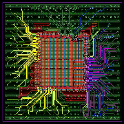
9 FC Sample Case-1 9
10 FC Sample Case-2 Die Pin Count: 3302 die pins Bump Pitch: 180um Package size: 45x45 mm BGA array: 44x44 with 1 mm pitch Key Design attributes 77 signals of 50 ohms, 85 differential pairs in HT section and 243 pairs in Analog section All the pairs are routed in 2 layers and maximum spacing maintained between the pairs to allow GND flow between the pairs Stitching vias added between the pairs with equal spacing from start to end of the routing For each power and GND balls in core area, maximum number of vias added to improve connection path between Die and BGA Differential pair P and N balls have given a common large oval void area to avoid sharp corners. HT signals are matched within 7ps tolerance Layers used structure (BU-C-BU) & Lead Time 2 weeks 10

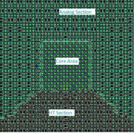
11 FC Sample Case-2 11

12 FC Sample Case-2 Power Layer 12
13 FC Sample Case-3 Die Pin Count: 1816 die pins Bump Pitch: 210 um Package size: 35x35 mm BGA array: 34x34 with 1 mm pitch Key Design attributes Design has different interfaces like DDR,XUAI, RGMII and PCIe TX and RX nets of XUAI and PCIe are routed in different layers DDR nets are routed as groups with 8 data bits and its strobe pair in the middle of each byte DDR signals are routed as byte with respect to their banks and length matched according to the skew requirements. XAUI, RGMII and PCIe Section also matched as per their skew requirements All the signals are routed with tight spacing and enough shielding was provided for all diff pairs For each power and GND balls in core area, 6 micro vias added to improve PDN performance Layers used structure (BU-C-BU) & Lead Time 2.5 weeks 13

14 FC Sample Case-3 14
15 FC Sample Case-4 Die Pin Count: DIE pins, DIE2-692 Bump Pitch: DIE1-400 um, DIE2 180um Package size: CBGA 25x25 mm BGA array: 24x24 with 1 mm pitch Key Design attributes Multi chip flip chip design with 2 DIE in a single substrate One die is analog & another is digital & connectivity achieved between 2 DIE using diff pairs 192 differential pairs in digital section and 188 pairs in analog section Design consists of XAUI and GPIO Section and they are routed per their routing specification. Analog and digital power/gnds are properly planned and plane pouring is done without interference of each other Core area of Digital DIE have different powers and achieving connectivity was difficult task Layers used 12 layers and Lead Time 3 weeks 15

16 FC Sample Case-4 16
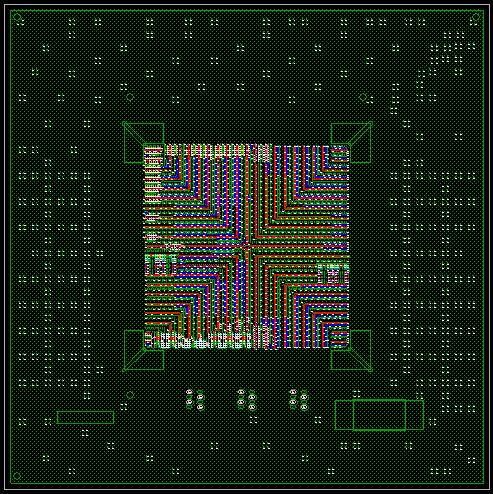
17 FC Sample Case-5 Die Pin Count: 1923 Die pins Bump Pitch: 169 um Package size: 21x21 mm BGA array: 25x25 with 0.8 mm pitch Key Design attributes Design has different interfaces like DDR3,GMII, PCIe, SPI, QSPI, USB Differential Pairs are routed such that the intra-pair skew is <=2ps. CLK signals surrounded by GND shielding traces and stitching vias. GND vias are present as near as possible to the end of each signal to provide return path. Differential traces and critical signal traces are not routed above or below degassing holes. Core power and GND vias are placed wherever possible underneath the die to minimize voltage drop. Core area fanout with different powers and achieving connectivity was difficult task. Layers used 4 layers & Lead time-1.5 weeks 17


18 FC Sample Case-5 COMPLEX CORE AREA 18
19 FC Sample Case-6 Die Pin Count: 6355 Die pins Bump Pitch: 148 um Package size: 37.5x37.5 mm BGA array: 36x36 with 1.0 mm pitch Key Design attributes Design has different interfaces like DDR3,I2C, PCIe, and few other high speed signals 551 Ios and among them 294 are differential pair signals. More than 2x spacing maintained between the signals outside of die area All the high speed signals and differential pairs are routed with 3x spacing from other IOs. Signals are routed carefully such that each group of signals are given its corresponding power as reference in the adjacent layer. BGA fanout pattern was created in such a way to avoid sharp edges in the shapes Layers used 10 layers & Lead time - 2 weeks 19

20 FC Sample Case-6 20

21 WB Sample Case-1 Die Pin Count: 689 die pins in 2 rows Package size: 31x31 mm BGA array: 1289 ball pins with 1 mm pitch Key Design attributes 241 Ios with different interfaces like DDR,GPIO,I2C,SPI,USB and others Differential pairs are routed with 5x spacing to other signals GND shielding traces added on both sides of critical signals Each group of signals is routed with its corresponding GND reference in GND layer Power rings created for 4 powers and 2 GND. Layers used 4 layers Lead Time 1.5 weeks 21

22 WB Sample Case-1 22
23 WB Sample Case-2 Die Pin Count: 292 die pins Package size: 27x27 mm BGA array: 484 pin perimeter matrix BGA with 1 mm pitch Key Design attributes 316 Ios with different interfaces like DDR,GMII,MII,GPIO and other interfaces Routing done in any angle trace to reduce length and to increase space for routing all signals in Top layer TX and RX pairs are routed with their respective GND shielding traces on both sides of the pairs and the same GND is given as reference in immediate next layer Due to spacing constraints, 2 nd row of bond finger is created for few signals and connected to nearest ball pin. Power ring created for 3 different powers and vias are connected to its power plane. Plating tails added for all nets Layers used 4 layers and Lead Time 2 weeks 23

24 WB Sample Case-2 24
25 WB Sample Case-3 Die Pin Count: 365 die pins Package size: 21x21 mm BGA array: 365 pin perimeter matrix HSBGA with 1 mm pitch Key Design attributes 226 Ios with Analog, Digital and HDMI section and among them 4 are differential pairs in HDMI All the signals are routed in Top layer with its respective GND as reference Staggered Bond finger pattern created for signals and few power and GND pins 4 Power rings created for 5 powers and 3 GND nets. Sunray pattern added to core ground ring Plating tails added for all nets Fiducials placed as per requirement and connected to GND Layers used 4 layers Lead Time 2 weeks 25

26 WB Sample Case-3 26

27 WB Sample Case-3 27
28 PACKAGE SI & PI SIMULATION 28
29 SIMULATION CAPABILITES Pre-layout Analysis - Define Specification & Stack-Up Verification - Length tolerance, Impedance, etc - Can model diffpair and SE signals separately for loss analysis - Can analyze crosstalk for different spacing Post-layout Analysis - S-parameter and TDR analysis - Reflection analysis and Xtalk - Eye diagram and BER calculation - RLC parasitic Calculation - Crosstalk Checking - BUS simulation for timing budget calculation 29
30 SIGNAL INTEGRITY CO-DESIGN SIGNAL INTEGRITY POWER INTEGRITY EMI/EMC Minimize-cost & Maximize Performance 30
 AC Analysis ( PDN impedance analysis, target impedance optimization,")
31 SERVICES Signal Integrity Power Integrity Pre layout & Post layout Serial & parallel interface (DDR 2/3/4, gigabit-serdes) Co-design (IC/package/board) IBIS/IBIS-AMI based system SI Crosstalk, channel loss, s-parameter, eye-diagram, timing analysis DC Analysis (IR drop, voltage/current distribution, density plots) AC Analysis ( PDN impedance analysis, target impedance optimization, Transient noise estimation) Decoupling cap analysis & optimization EMI/EMC EMI Radiation EMI Susceptibility Compliances to various EMI standards during design phase Simulation Tools Cadence Sigrity PowerDC, PowerSI, Optimize PI, Xtract IM Ansys HFSS, Siwave, Designer Agilent ADS 31
 using high frequent dielectric materials like ABF-GX13 prepreg and E700GR core materials.")

32 PACKAGE DESIGN CASE ANALYSIS Flip chip design with 5043 die pins. 32x32 (1024 BGA pins) BGA array with 1 mm pitch. Layers used : structure (BU-C-BU) using high frequent dielectric materials like ABF-GX13 prepreg and E700GR core materials. Copper material is used. Critical power net VDD : 1.5V, 5A This design high frequency SERDES signals like Group Net name Freq. SerDes CPRI_SERDES_RXP0,CPRI_SERDES_RXN GHZ SerDes CPRI_SERDES_RXP1,CPRI_SERDES_RXN GHZ SerDes CPRI_SERDES_TXP0,CPRI_SERDES_TXN GHZ SerDes CPRI_SERDES_TXP1,CPRI_SERDES_TXN GHZ 32

33 PACKAGE DESIGN CASE ANALYSIS S-Parameter Analysis for 5.06 GHz SERDES channel HFSS 3Dmodel & Insertion Loss 33
34 PACKAGE DESIGN CASE ANALYSIS S-Parameter Analysis for 5.06 GHz SERDES channel HFSS 3D model & Return Loss 34

35 S-PARAMETER SIMULATION 10 Layers Package design DIE pins & 1935 BGA pins Insertion & Return loss calculation up to 10GHz using ANSYS Siwave tool. 35

36 RLC Extraction & IBIS pin model 2354 DIE pins & 400 BGA pins. Extracting Net based RLC values. Pin model with RLC values for the IBIS model. Tool used XTRACTPI 36
37 POWER INTEGRITY ANALYSIS IR drop analysis to find voltage drop for plane and pins and to find the hot spot areas Power/GND Impedance profile analysis The target impedance is useful for sizing the amount of capacitance necessary at each level of assembly to store sufficient charge and energy for the load. De-coupling Capacitors Estimation and Optimization It is necessary to analyze and optimize the exact number and values of capacitors needed in order to achieve the desired PDN Power Plane RLC Proper control in the plane RLC value gives good power impedance with less IR drop. 37
38 PACKAGE DESIGN CASE ANALYSIS CASE1 : DC Analysis Block Diagram Result 38

39 PACKAGE DESIGN CASE ANALYSIS Voltage distribution of VDD, VDDA & VDDHT Power nets DDRVDDQ Voltage distribution plot 39

40 PACKAGE DESIGN CASE ANALYSIS Current density of VDD, VDDA & VDDHT Power nets 40
41 PACKAGE DESIGN CASE Z11 analysis for VDD power net ANALYSIS 41

42 DECAP OPTIMIZATION 10 Layers Package design DIE pins & 1088 BGA pins. Finding the optimized Decap scheme for obtaining the least impedance of a power net. Simulated using the PiAdvisor option in the ANSYS Siwave tool 42

43 Geographical Location Headquarters at Coimbatore, Tamil Nadu. Southern part of India. - Near to Bangalore & Chennai - 2nd best industrial city in Tamil Nadu Development Centers at Bangalore & Chennai Sales Office at USA & Japan 43

44 Contact Details M/S No.6, 1 st Street, Gandhi Nagar Kavundampalayam, Coimbatore - 30, TN, India. Phone: info@caliberinterconnect.com 44
45 Our Locations Coimbatore No 6, 1 st Street, Gandhi Nagar Kavundampalayam, Coimbatore , Tamilnadu, India. Directline: Fax: Chennai 157, First Floor, 10th Cross Street, C.L.R.I. Nagar, Neelankarai, Chennai , Tamilnadu, India. Phone: Bangalore No.362,12 th Main Road, Hosur Sarjapur Road, Sector-5, HSR Layout, Bangalore , Karnataka, India. Directline: JAPAN Mr.Kimiaki Tanaka, Ogikubo, Suginamiku, Tokyo , Japan, Phone: USA 4647, Carmen Ct, Union City-94857, California,USA Phone:

46 Thank You!! Contact us Visit us at 46
Caliber Interconnect Solutions
 Caliber Interconnect Solutions Design for perfection CASE STUDY DBFSP card and Optical card Transceivers Channels (through Backplane) Pre-Layout SI Report Caliber Interconnect Solutions (Pvt) Ltd No 6,1
How to anticipate Signal Integrity Issues: Improve my Channel Simulation by using Electromagnetic based model
 How to anticipate Signal Integrity Issues: Improve my Channel Simulation by using Electromagnetic based model HSD Strategic Intent Provide the industry s premier HSD EDA software. Integration of premier
ANSYS CPS SOLUTION FOR SIGNAL AND POWER INTEGRITY
 ANSYS CPS SOLUTION FOR SIGNAL AND POWER INTEGRITY Rémy FERNANDES Lead Application Engineer ANSYS 1 2018 ANSYS, Inc. February 2, 2018 ANSYS ANSYS - Engineering simulation software leader Our industry reach
System Co-design and optimization for high performance and low power SoC s
 System Co-design and optimization for high performance and low power SoC s Siva S Kothamasu, Texas Instruments Inc, Dallas Snehamay Sinha, Texas Instruments Inc, Dallas Amit Brahme, Texas Instruments India
through Electrical Performance Assessment Principal AE Aug
 An Alternative for Design Checking through Electrical Performance A Assessment t y Wu Paddy Principal AE Aug.13 2013 Agenda The Package/PCB Electrical Performance Checking Challenge Allegro Sigrity Integration
Relationship Between Signal Integrity and EMC
 Relationship Between Signal Integrity and EMC Presented by Hasnain Syed Solectron USA, Inc. RTP, North Carolina Email: HasnainSyed@solectron.com 06/05/2007 Hasnain Syed 1 What is Signal Integrity (SI)?
Si-Interposer Collaboration in IC/PKG/SI. Eric Chen
 Si-Interposer Collaboration in IC/PKG/SI Eric Chen 4/Jul/2014 Design Overview U-bump Logic IC Mem IC C4 bump Logic IC Silicon/Organic substrate Interposer Mem IC CAP Package substrate Solder Ball VRM BGA
Signal Integrity Modeling and Simulation for IC/Package Co-Design
 Signal Integrity Modeling and Simulation for IC/Package Co-Design Ching-Chao Huang Optimal Corp. October 24, 2004 Why IC and package co-design? The same IC in different packages may not work Package is
The Design Challenge to Integrate High Performance Organic Packaging into High End ASIC Strategic Space Based Applications.
 The Design Challenge to Integrate High Performance Organic Packaging into High End ASIC Strategic Space Based Applications May 8, 2007 Abstract: The challenge to integrate high-end, build-up organic packaging
Considerations in High-Speed High Performance Die-Package-Board Co-Design. Jenny Jiang Altera Packaging Department October 2014
 Considerations in High-Speed High Performance Die-Package-Board Co-Design Jenny Jiang Altera Packaging Department October 2014 Why Co-Design? Complex Multi-Layer BGA Package Horizontal and vertical design
Source: Nanju Na Jean Audet David R Stauffer IBM Systems and Technology Group
 Title: Package Model Proposal Source: Nanju Na (nananju@us.ibm.com) Jean Audet (jaudet@ca.ibm.com), David R Stauffer (dstauffe@us.ibm.com) Date: Dec 27 IBM Systems and Technology Group Abstract: New package
PI3DPX1207B Layout Guideline. Table of Contents. 1 Layout Design Guideline Power and GROUND High-speed Signal Routing...
 PI3DPX1207B Layout Guideline Table of Contents 1 Layout Design Guideline... 2 1.1 Power and GROUND... 2 1.2 High-speed Signal Routing... 3 2 PI3DPX1207B EVB layout... 8 3 Related Reference... 8 Page 1
Intro. to PDN Planning PCB Stackup Technology Series
 Introduction to Power Distribution Network (PDN) Planning Bill Hargin In-Circuit Design b.hargin@icd.com.au 425-301-4425 Intro. to PDN Planning 1. Intro/Overview 2. Bypass/Decoupling Strategy 3. Plane
PDS Impact for DDR Low Cost Design
 PDS Impact for DDR3-1600 Low Cost Design Jack W.C. Lin Sr. AE Manager jackl@cadence.com Aug. g 13 2013 Cadence, OrCAD, Allegro, Sigrity and the Cadence logo are trademarks of Cadence Design Systems, Inc.
EMI Reduction on an Automotive Microcontroller
 EMI Reduction on an Automotive Microcontroller Design Automation Conference, July 26 th -31 st, 2009 Patrice JOUBERT DORIOL 1, Yamarita VILLAVICENCIO 2, Cristiano FORZAN 1, Mario ROTIGNI 1, Giovanni GRAZIOSI
PCB Routing Guidelines for Signal Integrity and Power Integrity
 PCB Routing Guidelines for Signal Integrity and Power Integrity Presentation by Chris Heard Orange County chapter meeting November 18, 2015 1 Agenda Insertion Loss 101 PCB Design Guidelines For SI Simulation
Microcircuit Electrical Issues
 Microcircuit Electrical Issues Distortion The frequency at which transmitted power has dropped to 50 percent of the injected power is called the "3 db" point and is used to define the bandwidth of the
Plane Crazy, Part 2 BEYOND DESIGN. by Barry Olney
 by Barry Olney column BEYOND DESIGN Plane Crazy, Part 2 In my recent four-part series on stackup planning, I described the best configurations for various stackup requirements. But I did not have the opportunity
NextGIn( Connec&on'to'the'Next'Level' Application note // DRAFT Fan-out 0,50mm stapitch BGA using VeCS. Joan Tourné NextGIn Technology BV
 NextGIn( Connec&on'to'the'Next'Level' Application note // DRAFT Fan-out 0,50mm stapitch BGA using VeCS. Joan Tourné NextGIn Technology BV February 27 th 2017 In this document we describe the use of VeCS
Effect of Power Noise on Multi-Gigabit Serial Links
 Effect of Power Noise on Multi-Gigabit Serial Links Ken Willis (kwillis@sigrity.com) Kumar Keshavan (ckumar@sigrity.com) Jack Lin (jackwclin@sigrity.com) Tariq Abou-Jeyab (tariqa@sigrity.com) Sigrity Inc.,
PDN design and analysis methodology in SI&PI codesign
 PDN design and analysis methodology in SI&PI codesign www.huawei.com Asian IBIS Summit, November 9, 2010, Shenzhen China Luo Zipeng (luozipeng@huawei.com) Liu Shuyao (liushuyao@huawei.com) HUAWEI TECHNOLOGIES
Introduction to EMI/EMC Challenges and Their Solution
 Introduction to EMI/EMC Challenges and Their Solution Dr. Hany Fahmy HSD Application Expert Agilent Technologies Davy Pissort, K.U. Leuven Charles Jackson, Nvidia Charlie Shu, Nvidia Chen Wang, Nvidia
Automotive PCB SI and PI analysis
 Automotive PCB SI and PI analysis SI PI Analysis Signal Integrity S-Parameter Timing analysis Eye diagram Power Integrity Loop / Partial inductance DC IR-Drop AC PDN Impedance Power Aware SI Signal Integrity
EMI/EMC of Entire Automotive Vehicles and Critical PCB s. Makoto Suzuki Ansoft Corporation
 EMI/EMC of Entire Automotive Vehicles and Critical PCB s Makoto Suzuki Ansoft Corporation WT10_SI EMI/EMC of Entire Automotive Vehicles and Critical PCB s Akira Ohta, Toru Watanabe, Benson Wei Makoto Suzuki
User2User The 2007 Mentor Graphics International User Conference
 7/2/2007 1 Designing High Speed Printed Circuit Boards Using DxDesigner and Expedition Robert Navarro Jet Propulsion Laboratory, California Institute of Technology. User2User The 2007 Mentor Graphics International
Electrical Test Vehicle for High Density Fan-Out WLP for Mobile Application. Institute of Microelectronics 22 April 2014
 Electrical Test Vehicle for High Density Fan-Out WLP for Mobile Application Institute of Microelectronics 22 April 2014 Challenges for HD Fan-Out Electrical Design 15-20 mm 7 mm 6 mm SI/PI with multilayer
March 6-9, 2016 Hilton Phoenix / Mesa Hotel Mesa, Arizona Archive- Session 4
 Proceedings Archive March 6-9, 2016 Hilton Phoenix / Mesa Hotel Mesa, Arizona Archive- Session 4 2016 BiTS Workshop Image: Stiop / Dollarphotoclub Proceedings Archive Presentation / Copyright Notice The
Why do we need to study Signal Integrity, Power Integrity and EMI ALL-AT-ONCE?
 Why do we need to study Signal Integrity, Power Integrity and EMI ALL-AT-ONCE? Hany Fahmy Riccardo Giacometti Cédric Pujol EMI HSD Signal Integrity Power Integrity An Example of Dramatic increase in HSD
Signal Integrity Design of TSV-Based 3D IC
 Signal Integrity Design of TSV-Based 3D IC October 24, 21 Joungho Kim at KAIST joungho@ee.kaist.ac.kr http://tera.kaist.ac.kr 1 Contents 1) Driving Forces of TSV based 3D IC 2) Signal Integrity Issues
CPS-1848 PCB Design Application Note
 Titl CPS-1848 PCB Design Application Note June 22, 2010 6024 Silver Creek Valley Road, San Jose, California 95138 Telephone: (408) 284-8200 Fax: (408) 284-3572 2010 About this Document This document is
Introduction to Board Level Simulation and the PCB Design Process
 BEYOND DESIGN C O L U M N Introduction to Board Level Simulation and the PCB Design Process by Barry Olney IN-CIRCUIT DESIGN PTY LTD AUSTRALIA SUMMARY Board-level simulation reduces costs by identifying
FPGA World Conference Stockholm 08 September John Steinar Johnsen -Josse- Senior Technical Advisor
 FPGA World Conference Stockholm 08 September 2015 John Steinar Johnsen -Josse- Senior Technical Advisor Agenda FPGA World Conference Stockholm 08 September 2015 - IPC 4101C Materials - Routing out from
Split Planes in Multilayer PCBs
 by Barry Olney coulmn BEYOND DESIGN Split Planes in Multilayer PCBs Creating split planes or isolated islands in the copper planes of multilayer PCBs at first seems like a good idea. Today s high-speed
Power Distribution Network Design for Stratix IV GX and Arria II GX FPGAs
 Power Distribution Network Design for Stratix IV GX and Arria II GX FPGAs Transceiver Portfolio Workshops 2009 Question What is Your PDN Design Methodology? Easy Complex Historical Full SPICE simulation
Silicon Interposers enable high performance capacitors
 Interposers between ICs and package substrates that contain thin film capacitors have been used previously in order to improve circuit performance. However, with the interconnect inductance due to wire
Intel 82566/82562V Layout Checklist (version 1.0)
") Intel 82566/82562V Layout Checklist (version 1.0) Project Name Fab Revision Date Designer Intel Contact SECTION CHECK ITEMS REMARKS DONE General Ethernet Controller Obtain the most recent product documentation
Intel 82566/82562V Layout Checklist (version 1.0) Project Name Fab Revision Date Designer Intel Contact SECTION CHECK ITEMS REMARKS DONE General Ethernet Controller Obtain the most recent product documentation
Design Considerations for Highly Integrated 3D SiP for Mobile Applications
 Design Considerations for Highly Integrated 3D SiP for Mobile Applications FDIP, CA October 26, 2008 Joungho Kim at KAIST joungho@ee.kaist.ac.kr http://tera.kaist.ac.kr Contents I. Market and future direction
Hardware Design Considerations for MKW41Z/31Z/21Z BLE and IEEE Device
 NXP Semiconductors Document Number: AN5377 Application Note Rev. 2, Hardware Design Considerations for MKW41Z/31Z/21Z BLE and IEEE 802.15.4 Device 1. Introduction This application note describes Printed
Closing the loop part 1: Why use simulation tools for high speed signal channel design?
 Closing the loop part 1: Why use simulation tools for high speed signal channel design? Riccardo Giacometti Application Engineer Agilent EEsof EDA Page 1 High Speed Digital Design Flow Pre-Layout w/channel
High Speed Design Issues and Jitter Estimation Techniques. Jai Narayan Tripathi
 High Speed Design Issues and Jitter Estimation Techniques Jai Narayan Tripathi (jainarayan.tripathi@st.com) Outline Part 1 High-speed Design Issues Signal Integrity Power Integrity Jitter Power Delivery
Manufacture and Performance of a Z-interconnect HDI Circuit Card Abstract Introduction
 Manufacture and Performance of a Z-interconnect HDI Circuit Card Michael Rowlands, Rabindra Das, John Lauffer, Voya Markovich EI (Endicott Interconnect Technologies) 1093 Clark Street, Endicott, NY 13760
Practical Limitations of State of the Art Passive Printed Circuit Board Power Delivery Networks for High Performance Compute Systems
 Practical Limitations of State of the Art Passive Printed Circuit Board Power Delivery Networks for High Performance Compute Systems Presented by Chad Smutzer Mayo Clinic Special Purpose Processor Development
EMI. Chris Herrick. Applications Engineer
 Fundamentals of EMI Chris Herrick Ansoft Applications Engineer Three Basic Elements of EMC Conduction Coupling process EMI source Emission Space & Field Conductive Capacitive Inductive Radiative Low, Middle
3D IC-Package-Board Co-analysis using 3D EM Simulation for Mobile Applications
 3D IC-Package-Board Co-analysis using 3D EM Simulation for Mobile Applications Darryl Kostka, CST of America Taigon Song and Sung Kyu Lim, Georgia Institute of Technology Outline Introduction TSV Array
Texas Instruments DisplayPort Design Guide
 Texas Instruments DisplayPort Design Guide April 2009 1 High Speed Interface Applications Introduction This application note presents design guidelines, helping users of Texas Instruments DisplayPort devices
SIGNAL INTEGRITY ANALYSIS AND MODELING
 1.00mm Pitch BGA Socket Adapter System SIGNAL INTEGRITY ANALYSIS AND MODELING Rev. 2 www.advanced.com Signal Integrity Data Reporting At Advanced Interconnections Corporation, our Signal Integrity reporting
DL-150 The Ten Habits of Highly Successful Designers. or Design for Speed: A Designer s Survival Guide to Signal Integrity
 Slide -1 Ten Habits of Highly Successful Board Designers or Design for Speed: A Designer s Survival Guide to Signal Integrity with Dr. Eric Bogatin, Signal Integrity Evangelist, Bogatin Enterprises, www.bethesignal.com
Chapter 16 PCB Layout and Stackup
 Chapter 16 PCB Layout and Stackup Electromagnetic Compatibility Engineering by Henry W. Ott Foreword The PCB represents the physical implementation of the schematic. The proper design and layout of a printed
Multilayer PCB Stackup Planning
 by Barry Olney In-Circuit Design Pty Ltd Australia This Application Note details tried and proven techniques for planning high speed Multilayer PCB Stackup configurations. Planning the multilayer PCB stackup
AN-1370 APPLICATION NOTE
 APPLICATION NOTE One Technology Way P.O. Box 9106 Norwood, MA 02062-9106, U.S.A. Tel: 781.329.4700 Fax: 781.461.3113 www.analog.com Design Implementation of the ADF7242 Pmod Evaluation Board Using the
CMT2300AW Schematic and PCB Layout Design Guideline
 AN141 CMT2300AW Schematic and PCB Layout Design Guideline Introduction This document is the CMT2300AW Application Development Guideline. It will explain how to design and use the CMT2300AW schematic and
Power integrity is more than decoupling capacitors The Power Integrity Ecosystem. Keysight HSD Seminar Mastering SI & PI Design
 Power integrity is more than decoupling capacitors The Power Integrity Ecosystem Keysight HSD Seminar Mastering SI & PI Design Signal Integrity Power Integrity SI and PI Eco-System Keysight Technologies
Fan-Out Solutions: Today, Tomorrow the Future Ron Huemoeller
 Fan-Out Solutions: Today, Tomorrow the Future Ron Huemoeller Corporate Vice President, WW RnD & Technology Strategy 1 In the Beginning ewlb 2 Fan Out Packaging Emerges Introduction of Fan Out (ewlb) Marketed
PI3HDMIxxx 4-Layer PCB Layout Guideline for HDMI Products
 PI3HDMIxxx 4-Layer PCB Layout Guideline for HDMI Products Introduction The differential trace impedance of HDMI is specified at 100Ω±15% in Test ID 8-8 in HDMI Compliance Test Specification Rev.1.2a and
Engineering the Power Delivery Network
 C HAPTER 1 Engineering the Power Delivery Network 1.1 What Is the Power Delivery Network (PDN) and Why Should I Care? The power delivery network consists of all the interconnects in the power supply path
Differential Pair Routing
 C O L U M N BEYOND DESIGN Differential Pair Routing by Barry Olney IN-CIRCUIT DESIGN PTY LTD, AUSTRALIA A differential pair is two complementary transmission lines that transfer equal and opposite signals
Reliable World Class Insights Your Silicon Valley Partner in Simulation ANSYS Sales, Consulting, Training & Support
 www.ozeninc.com info@ozeninc.com (408) 732 4665 1210 E Arques Ave St 207 Sunnyvale, CA 94085 Reliable World Class Insights Your Silicon Valley Partner in Simulation ANSYS Sales, Consulting, Training &
Quick guide to Power. V1.2.1 July 29 th 2013
 Quick guide to Power Distribution ib ti Network Design V1.2.1 July 29 th 2013 High level High current, high transient Power Distribution Networks (PDN) need to be able to respond to changes and transients
DP Array DPAM/DPAF Final Inch Designs in Serial ATA Generation 1 Applications 10mm Stack Height. REVISION DATE: January 11, 2005
 Application Note DP Array DPAM/DPAF Final Inch Designs in Serial ATA Generation 1 Applications 10mm Stack Height REVISION DATE: January 11, 2005 Copyrights and Trademarks Copyright 2005 Samtec, Inc. Developed
Chip Package - PC Board Co-Design: Applying a Chip Power Model in System Power Integrity Analysis
 Chip Package - PC Board Co-Design: Applying a Chip Power Model in System Power Integrity Analysis Authors: Rick Brooks, Cisco, ricbrook@cisco.com Jane Lim, Cisco, honglim@cisco.com Udupi Harisharan, Cisco,
Signal Integrity for Gigascale SOC Design. Professor Lei He ECE Department University of Wisconsin, Madison
 Signal Integrity for Gigascale SOC Design Professor Lei He ECE Department University of Wisconsin, Madison he@ece.wisc.edu http://eda.ece.wisc.edu Outline Capacitive noise Technology trends Capacitance
Sherlock Solder Models
 Introduction: Sherlock Solder Models Solder fatigue calculations in Sherlock are accomplished using one of the many solder models available. The different solder models address the type of package that
DL-150 The Ten Habits of Highly Successful Designers. or Design for Speed: A Designer s Survival Guide to Signal Integrity
 Slide -1 Ten Habits of Highly Successful Board Designers or Design for Speed: A Designer s Survival Guide to Signal Integrity with Dr. Eric Bogatin, Signal Integrity Evangelist, Bogatin Enterprises, www.bethesignal.com
Design Guide for High-Speed Controlled Impedance Circuit Boards
 IPC-2141A ASSOCIATION CONNECTING ELECTRONICS INDUSTRIES Design Guide for High-Speed Controlled Impedance Circuit Boards Developed by the IPC Controlled Impedance Task Group (D-21c) of the High Speed/High
Demystifying Vias in High-Speed PCB Design
 Demystifying Vias in High-Speed PCB Design Keysight HSD Seminar Mastering SI & PI Design db(s21) E H What is Via? Vertical Interconnect Access (VIA) An electrical connection between layers to pass a signal
The Inductance Loop Power Distribution in the Semiconductor Test Interface. Jason Mroczkowski Multitest
 The Inductance Loop Power Distribution in the Semiconductor Test Interface Jason Mroczkowski Multitest j.mroczkowski@multitest.com Silicon Valley Test Conference 2010 1 Agenda Introduction to Power Delivery
CIRCUITS. Raj Nair Donald Bennett PRENTICE HALL
 POWER INTEGRITY ANALYSIS AND MANAGEMENT I CIRCUITS Raj Nair Donald Bennett PRENTICE HALL Upper Saddle River, NJ Boston Indianapolis San Francisco New York Toronto Montreal London Munich Paris Madrid Capetown
Decoupling capacitor placement
 Decoupling capacitor placement Covered in this topic: Introduction Which locations need decoupling caps? IC decoupling Capacitor lumped model How to maximize the effectiveness of a decoupling cap Parallel
High-Speed Differential Interconnection Design for Flip-Chip BGA Packages
 High-Speed Differential Interconnection Design for Flip-Chip BGA Packages W.L. Yuan, H.P. Kuah, C.K. Wang, Anthony Y.S. Sun W.H. Zhu, H.B. Tan, and A.D. Muhamad Packaging Analysis and Design Center United
A Simulation Study of Simultaneous Switching Noise
 A Simulation Study of Simultaneous Switching Noise Chi-Te Chen 1, Jin Zhao 2, Qinglun Chen 1 1 Intel Corporation Network Communication Group, LOC4/19, 9750 Goethe Road, Sacramento, CA 95827 Tel: 916-854-1178,
A Co-design Methodology of Signal Integrity and Power Integrity
 DesignCon 2006 A Co-design Methodology of Signal Integrity and Power Integrity Woong Hwan Ryu, Intel Corporation woong.hwan.ryu@intel.com Min Wang, Intel Corporation min.wang@intel.com 1 Abstract As PCB
Digital Integrated Circuits Lecture 20: Package, Power, Clock, and I/O
 Digital Integrated Circuits Lecture 20: Package, Power, Clock, and I/O Chih-Wei Liu VLSI Signal Processing LAB National Chiao Tung University cwliu@twins.ee.nctu.edu.tw DIC-Lec20 cwliu@twins.ee.nctu.edu.tw
MICROELECTRONICS ASSSEMBLY TECHNOLOGIES. The QFN Platform as a Chip Packaging Foundation
 West Coast Luncheon January 15, 2014. PROMEX PROMEX INDUSTRIES INC. MICROELECTRONICS ASSSEMBLY TECHNOLOGIES The QFN Platform as a Chip Packaging Foundation 3075 Oakmead Village Drive Santa Clara CA Ɩ 95051
Learning the Curve BEYOND DESIGN. by Barry Olney
 by Barry Olney coulmn BEYOND DESIGN Learning the Curve Currently, power integrity is just entering the mainstream market phase of the technology adoption life cycle. The early market is dominated by innovators
EMC for Printed Circuit Boards
 9 Bracken View, Brocton Stafford, Staffs, UK tel: +44 (0)1785 660 247 fax +44 (0)1785 660 247 email: keith.armstrong@cherryclough.com web: www.cherryclough.com EMC for Printed Circuit Boards Basic and
True Differential IBIS model for SerDes Analog Buffer
 True Differential IBIS model for SerDes Analog Buffer Shivani Sharma, Tushar Malik, Taranjit Kukal IBIS Asia Summit Shanghai, China Nov. 14, 2014 Agenda Overview of Differential IBIS Description of test-case
The amout, type and position definition and optimization of decoupling capacitors which depend on the resonance hot spot position,
 Resonance Simulation in PI Design Xiao Dan Nokia Abstract PCB power-ground resonance theory is introduced and relationship between Z simulated parameter and resonance frequency is discussed based on the
Overcoming the Challenges of HDI Design
 ALTIUMLIVE 2018: Overcoming the Challenges of HDI Design Susy Webb Design Science Sr PCB Designer San Diego Oct, 2018 1 Challenges HDI Challenges Building the uvia structures The cost of HDI (types) boards
Design Services Capability WiWo Tech Systems Pvt Ltd
 iotech Design Services Capability io Tech Pvt Ltd Company Profile iotech iotech Private Ltd is an Engineering design services company located in Bangalore iotech supports Engineering design services in
Webinar: Suppressing BGAs and/or multiple DC rails Keith Armstrong. 1of 5
 1of 5 Suppressing ICs with BGA packages and multiple DC rails Some Intel Core i5 BGA packages CEng, EurIng, FIET, Senior MIEEE, ACGI Presenter Contact Info email: keith.armstrong@cherryclough.com website:
The Challenges of Differential Bus Design
 The Challenges of Differential Bus Design February 20, 2002 presented by: Arthur Fraser TechKnowledge Page 1 Introduction Background Historically, differential interconnects were often twisted wire pairs
AMCHIP5 characterization tests
 AMCHIP6 status AMCHIP5 characterization tests Characterization results demonstrate the functionality of the AMCHIP5 @ 2 Gbit with a single event and by using the XORAM cell LV_cell seems to have some issue
QPI-AN1 GENERAL APPLICATION NOTE QPI FAMILY BUS SUPPLY QPI CONVERTER
 QPI-AN1 GENERAL APPLICATION NOTE QPI FAMILY EMI control is a complex design task that is highly dependent on many design elements. Like passive filters, active filters for conducted noise require careful
!"#$"%&' ()#*+,-+.&/0(
#*+,-+.&/0(") !"#$"%&' ()#*+,-+.&/0( Multi Chip Modules (MCM) or Multi chip packaging Industry s first MCM from IBM. Generally MCMs are horizontal or two-dimensional modules. Defined as a single unit containing two
!"#$"%&' ()#*+,-+.&/0( Multi Chip Modules (MCM) or Multi chip packaging Industry s first MCM from IBM. Generally MCMs are horizontal or two-dimensional modules. Defined as a single unit containing two
Touchstone v2.0 SI/PI S- Parameter Models for Simultaneous Switching Noise (SSN) Analysis of DDR4 Memory Interface Applications.
 Analysis of DDR4 Memory Interface Applications.") DesignCon 2014 Touchstone v2.0 SI/PI S- Parameter Models for Simultaneous Switching Noise (SSN) Analysis of DDR4 Memory Interface Applications. Romi Mayder, Xilinx, Inc. romi.mayder@xilinx.com Raymond
DesignCon 2014 Touchstone v2.0 SI/PI S- Parameter Models for Simultaneous Switching Noise (SSN) Analysis of DDR4 Memory Interface Applications. Romi Mayder, Xilinx, Inc. romi.mayder@xilinx.com Raymond
Enabling Parallel Testing at Sort for High Power Products
 Enabling Parallel Testing at Sort for High Power Products Abdel Abdelrahman Tim Swettlen 2200 Mission College Blvd. M/S SC2-07 Santa Clara, CA 94536 Abdel.Abdelrahman@intel.com Tim.Swettlen@intel.com Agenda
Low Jitter, Low Emission Timing Solutions For High Speed Digital Systems. A Design Methodology
 Low Jitter, Low Emission Timing Solutions For High Speed Digital Systems A Design Methodology The Challenges of High Speed Digital Clock Design In high speed applications, the faster the signal moves through
Bridging the Measurement and Simulation Gap Sarah Boen Marketing Manager Tektronix
 Bridging the Measurement and Simulation Gap Sarah Boen Marketing Manager Tektronix 1 Agenda Synergy between simulation and lab based measurements IBIS-AMI overview Simulation and measurement correlation
ECE 546 Introduction
 ECE 546 Introduction Spring 2018 Jose E. Schutt-Aine Electrical & Computer Engineering University of Illinois jesa@illinois.edu ECE 546 Jose Schutt Aine 1 Future System Needs and Functions Auto Digital
1 Introduction External Component Requirements AC Coupling Capacitors on high speed lanes... 2
 PI3TB212 PI3TB212 Thunderbolt Application Information Table of Contents 1 Introduction... 2 2 External Component Requirements... 2 2.1 AC Coupling Capacitors on high speed lanes... 2 2.2 Pull-down Resistor
Decoupling capacitor uses and selection
 Decoupling capacitor uses and selection Proper Decoupling Poor Decoupling Introduction Covered in this topic: 3 different uses of decoupling capacitors Why we need decoupling capacitors Power supply rail
MPC 5534 Case study. E. Sicard (1), B. Vrignon (2) Toulouse France. Contact : web site :
, B. Vrignon (2) Toulouse France. Contact : web site :") MPC 5534 Case study E. Sicard (1), B. Vrignon (2) (1) INSA-GEI, 135 Av de Rangueil 31077 Toulouse France (2) Freescale Semiconductors, Toulouse, France Contact : etienne.sicard@insa-toulouse.fr web site
MPC 5534 Case study E. Sicard (1), B. Vrignon (2) (1) INSA-GEI, 135 Av de Rangueil 31077 Toulouse France (2) Freescale Semiconductors, Toulouse, France Contact : etienne.sicard@insa-toulouse.fr web site
Vishram S. Pandit, Intel Corporation (916) ]
![Vishram S. Pandit, Intel Corporation (916) ]](/thumbs/72/66540527.jpg "Vishram S. Pandit, Intel Corporation (916) ]") DesignCon 2008 Simulation and Characterization of GHz On-Chip Power Delivery Network (PDN) Vishram S. Pandit, Intel Corporation [vishram.s.pandit@intel.com, (916)356-2059] Woong Hwan Ryu, Intel Corporation
DesignCon 2008 Simulation and Characterization of GHz On-Chip Power Delivery Network (PDN) Vishram S. Pandit, Intel Corporation [vishram.s.pandit@intel.com, (916)356-2059] Woong Hwan Ryu, Intel Corporation
100 Gb/s: The High Speed Connectivity Race is On
 100 Gb/s: The High Speed Connectivity Race is On Cathy Liu SerDes Architect, LSI Corporation Harold Gomard SerDes Product Manager, LSI Corporation October 6, 2010 Agenda 100 Gb/s Ethernet evolution SoC
AN 766: Intel Stratix 10 Devices, High Speed Signal Interface Layout Design Guideline
 AN 766: Intel Stratix 10 Devices, High Speed Signal Interface Layout Subscribe Latest document on the web: PDF HTML Contents Contents Intel Stratix 10 Devices, High Speed Signal Interface Layout... 3 Intel
TRINAT Amplifier-Shaper for Silicon Detector (TASS)
") Sept. 8, 20 L. Kurchaninov TRINAT Amplifier-Shaper for Silicon Detector (TASS). General description Preamplifier-shaper for TRINAT Si detector (Micron model BB) is charge-sensitive amplifier followed by
Sept. 8, 20 L. Kurchaninov TRINAT Amplifier-Shaper for Silicon Detector (TASS). General description Preamplifier-shaper for TRINAT Si detector (Micron model BB) is charge-sensitive amplifier followed by
Myoung Joon Choi, Vishram S. Pandit Intel Corp.
 Myoung Joon Choi, Vishram S. Pandit Intel Corp. IBIS Summit at DesignCon 2010 Acknowledgements: Woong Hwan Ryu, Joe Salmon Copyright 2010, Intel Corporation. All rights reserved. Need for SI/PI Co-analysis
High Speed Characterization Report
 QTH-030-01-L-D-A Mates with QSH-030-01-L-D-A Description: High Speed Ground Plane Header Board-to-Board, 0.5mm (.0197 ) Pitch, 5mm (.1969 ) Stack Height Samtec, Inc. 2005 All Rights Reserved Table of Contents
The 3D Silicon Leader
 The 3D Silicon Leader 3D Silicon IPD for smaller and more reliable Implantable Medical Devices ATW on Advanced Packaging for Wireless Medical Devices Mohamed Mehdi Jatlaoui, Sébastien Leruez, Olivier Gaborieau,
Q2 QMS-DP/QFS-DP Series 11 mm Stack Height Final Inch Designs in Serial ATA Generation 1 Applications. Revision Date: February 22, 2005
 Q2 QMS-DP/QFS-DP Series 11 mm Stack Height Final Inch Designs in Serial ATA Generation 1 Applications Revision Date: February 22, 2005 Copyrights and Trademarks Copyright 2005 Samtec, Inc. Developed in