Myoung Joon Choi, Vishram S. Pandit Intel Corp.
|
|
|
- Marshall Shaw
- 5 years ago
- Views:
Transcription
1 Myoung Joon Choi, Vishram S. Pandit Intel Corp. IBIS Summit at DesignCon 2010 Acknowledgements: Woong Hwan Ryu, Joe Salmon Copyright 2010, Intel Corporation. All rights reserved.
2 Need for SI/PI Co-analysis Ingredients for SI/PI analysis Controllable/ Uncontrollable Parameters Different Cases and Decomposition Linearity Indicator Summary 2
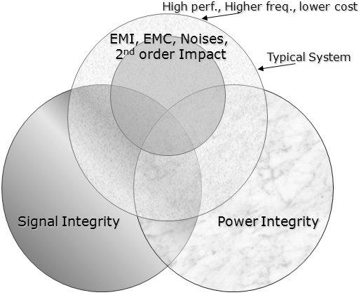
3 There are 3 major noise sources in the channel analysis Crosstalk, ISI, and SSO SI Only: Crosstalk and ISI; PI only: SSO For high speed low cost systems the separate analysis is not sufficient Second and third order effects become prominent. SI/PI co-analysis is becoming increasingly important. 3
4 Model Generation Passive Models PCB, Package, on-chip: 2D/ 3D EM Models Buffer Models: PD info in Buffer models Power Grid Models Pattern Generation Full time domain simulations Different cases for identifying 2 nd / 3 rd order effects Controllable parameters and their variations 4
5 Simplified On-chip Power Grid and On-chip PDN Capacitor with Buffer Connection and PDN noise impact on eye jitter 5
6 P G A: Source VRM PCB Connection to Package BGA Side Connections Package Bump Side Connections P G A PDN Model Grid, Pkg, PCB It needs to be with the SI channel models Coupling between power and signal needs to be considered during the modeling reference transition via coupling, etc. Ckt B: Load 6
7 Z11 profile at the Power node of Driver Simulated Noise at the Power node of Driver 0.20 mag(z(12,12)) freq, GHz PDN Noise analysis determines the noise at different data rates. This noise gets coupled to signals at the chip level. Interconnect impact needs to be determined by SI/PI analysis
8 Examples SI/PI Controllable Variables SI/PI Uncontrollable Variables Silicon Package/socket Ron, Slew rate, ODT, PDcap and Rdamp, Bumpout, I/O & EQ scheme, Power Grid Routing Trace width and spacing between lines, Pin-map, Referencing scheme I/O count, I/O device capacitor Unintentional PD Cap, Integrated passive element tolerances, Silicon process variations I/O pincount, Package manufacturing tolerances, Passive element tolerances, Stackup parameters (dielectric height and constant), Limited signal trace width and spacing PCB Trace width and spacing between lines, Rtt, Interconnect topology, Rs in memory channel, Referencing scheme PCB manufacturing tolerances, passive element tolerances, Stackup parameters (dielectric height and constant), Limited signal trace width and spacing DIMM/Connector Trace width and spacing between lines, Connector pinmap, Rtt, Interconnect topology, Stub resistor (Rstub), Referencing scheme Total I/O pincount, PCB manufacturing tolerances, Passive element tolerances, Stackup parameters (dielectric height and constant), Limited signal trace width and spacing 8
9 Combination of different cases can be run for SI/PI co-analysis Response Decomposition can be performed Forced Stimulus Setups for SI-PI Co-simulation Case # ISI Cross-talk SSO ISI SSO, ISI Cross-talk, ISI Cross-talk, ISI, SSO 1 Minimal Minimal Minimal 2 Yes Minimal Minimal 3 Minimal Minimal Yes 4 Yes Minimal Yes 5 Minimal Yes Minimal 6 Yes Yes Minimal 7 Minimal Yes Yes 8 Yes Yes Yes 9
10 Construction of ISI needs only one or more rising and falling edge. A lone bit excitation of ISI node for minimal ISI Eye construction by wrapping the waveform twice in time domain for the UI Delayed bits excitation of ISI node for minimal ISI Eye construction Delayed transition excitation of ISI node for minimal ISI Eye construction Radom Bit pattern for ISI 10


11 Minimal ISI only ISI and SSO ISI and Xtalk ISI, Xtalk, SSO
12 ustrip PDA Results Strip PDA(Peak Distortion Analysis) produce WC eye and WC patterns Full Time Domain SI-PI simulation might have eyes similar to PDA WC eye but the values are different because of SI-PI impact 12


13 ustrip Full Time Domain SI-PI Co-sim Results Ex Strip Full Time Domain SI-PI simulation might have eyes similar to PDA WC eye but the values are different because of SI-PI impact 13


14 Eye Diagram Measurement Scheme 14
15 15
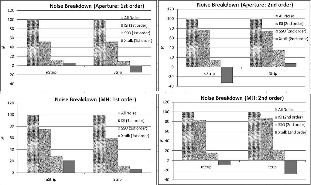
16 What is Linearity Indicator (LI)?? If you are doing SI-only or PI-only Sim/Analysis and LI>1 : you are overestimating noise LI<1 : you are underestimating noise Ratio of Eye degradation when analysis is done separately to that when it is done combined. 1 St order: Only 1 noise generating element 2 nd order: 2 noise generating elements Linearity (1st order) Linearity (2nd order) Outlier: Spec dependent ustrip Strip Aperture Based: Mh_based: Aperture Based: Mh_based:
17 17
18 It is system dependent Linearity goes down with more no. of SSO bits As s the frequency of operation goes up, the linearity suffers. Designer could underestimate noise higher frequency of operation 18
19 Pseudo-differential buffers driving differential channel More linear than Single ended in this example 19
20 Linearity (1st order) Linearity (2nd order) Diif. Sig. Ex Aperture Based: Mh_based: Linearity Indicator (LI) 0.94 LI for Mh Differential Channel st Order LI for Mh 2nd Order LI for Mh L.I. for Differential Channel is ~ 0.9 ie. It is close to 1 It implies that when SI/PI co-simulations are done, the EYE margin reduction is still more, than that compared to if it is done separately. However, the impact is smaller. (compared to single ended) 20
21 Differential signaling channel has LI close to ~1 Might not need SI-PI 21
22 Differential channel receiver eye s 1st order and 2nd order Noise interactions are more linear 22
23 Accuracy SI PI Icc(t) SI-PI co-simulation Single Ended Differential: Support is critical Convenience Automation Multiple Domain Power Support is critical 23
24 Running separate SI and PI simulations may underestimate the Eye Degradation Full time domain simulations for the system (end to end models required) Linearity Indicator Single Ended and Differential Systems are evaluated with SI/PI analysis Single Ended Channel L.I.~ 06 to 0.9 Differential Channel L.I.~ 0.9 For both scenarios, the combined analysis shows more Eye degradations than separate ones. But the effect is more prominent for Single ended channel. 24
25 25
26 Behavioral model construction for SI-PI co-simulation PDN SI-PI co-simulation compatible model with variable currents with variable power node voltages 26


27 Forced Stimulus Setups for SI-PI Co-simulation Case # ISI Cross-talk SSO ISI SSO, ISI Cross-talk, ISI Cross-talk, ISI, SSO 1 Minimal Minimal Minimal 2 Yes Minimal Minimal 3 Minimal Minimal Yes 4 Yes Minimal Yes 5 Minimal Yes Minimal 6 Yes Yes Minimal 7 Minimal Yes Yes 8 Yes Yes Yes 2/4/

28 One rising edge & One falling edge 2/4/
29 29
30 30

31 Differential channel receiver eye s 1 st order and 2 nd order Noise interactions are more linear 31
32 32
33 33

34 ... 34
35 . 35
SSO Noise, Eye Margin, and Jitter Characterization for I/O Power Integrity
 DESIGNCON 2009 SSO Noise, Eye Margin, and Jitter Characterization for I/O Power Integrity Vishram S. Pandit, Intel Corporation [vishram.s.pandit@intel.com, (916)356-2059] Ashish N. Pardiwala, Intel Corporation
Relationship Between Signal Integrity and EMC
 Relationship Between Signal Integrity and EMC Presented by Hasnain Syed Solectron USA, Inc. RTP, North Carolina Email: HasnainSyed@solectron.com 06/05/2007 Hasnain Syed 1 What is Signal Integrity (SI)?
PDN design and analysis methodology in SI&PI codesign
 PDN design and analysis methodology in SI&PI codesign www.huawei.com Asian IBIS Summit, November 9, 2010, Shenzhen China Luo Zipeng (luozipeng@huawei.com) Liu Shuyao (liushuyao@huawei.com) HUAWEI TECHNOLOGIES
PDS Impact for DDR Low Cost Design
 PDS Impact for DDR3-1600 Low Cost Design Jack W.C. Lin Sr. AE Manager jackl@cadence.com Aug. g 13 2013 Cadence, OrCAD, Allegro, Sigrity and the Cadence logo are trademarks of Cadence Design Systems, Inc.
Asian IBIS Summit, Tokyo, Japan
 Asian IBIS Summit, Tokyo, Japan Satoshi Nakamizo / 中溝哲士 12 Nov. 2018 Keysight Technologies Japan K.K. T h e d a t a e y e i s c l o s i n g 1600 3200 6400 Memory channel BW limited Rj improving slowly
POWER INTEGRITY INTERFACES FOR I/O. With Signal Integrity/ Power Integrity Co-Design. Vishram S. Pandit Woong Hwan Ryu Myoung Joon Choi
 POWER INTEGRITY FOR I/O INTERFACES With Signal Integrity/ Power Integrity Co-Design Vishram S. Pandit Woong Hwan Ryu Myoung Joon Choi Upper Saddle River, NJ Boston Indianapolis San Francisco New York Toronto
Considerations in High-Speed High Performance Die-Package-Board Co-Design. Jenny Jiang Altera Packaging Department October 2014
 Considerations in High-Speed High Performance Die-Package-Board Co-Design Jenny Jiang Altera Packaging Department October 2014 Why Co-Design? Complex Multi-Layer BGA Package Horizontal and vertical design
A Co-design Methodology of Signal Integrity and Power Integrity
 DesignCon 2006 A Co-design Methodology of Signal Integrity and Power Integrity Woong Hwan Ryu, Intel Corporation woong.hwan.ryu@intel.com Min Wang, Intel Corporation min.wang@intel.com 1 Abstract As PCB
ANSYS CPS SOLUTION FOR SIGNAL AND POWER INTEGRITY
 ANSYS CPS SOLUTION FOR SIGNAL AND POWER INTEGRITY Rémy FERNANDES Lead Application Engineer ANSYS 1 2018 ANSYS, Inc. February 2, 2018 ANSYS ANSYS - Engineering simulation software leader Our industry reach
Vishram S. Pandit, Intel Corporation (916) ]
![Vishram S. Pandit, Intel Corporation (916) ]](/thumbs/72/66540527.jpg "Vishram S. Pandit, Intel Corporation (916) ]") DesignCon 2008 Simulation and Characterization of GHz On-Chip Power Delivery Network (PDN) Vishram S. Pandit, Intel Corporation [vishram.s.pandit@intel.com, (916)356-2059] Woong Hwan Ryu, Intel Corporation
DesignCon 2008 Simulation and Characterization of GHz On-Chip Power Delivery Network (PDN) Vishram S. Pandit, Intel Corporation [vishram.s.pandit@intel.com, (916)356-2059] Woong Hwan Ryu, Intel Corporation
100 Gb/s: The High Speed Connectivity Race is On
 100 Gb/s: The High Speed Connectivity Race is On Cathy Liu SerDes Architect, LSI Corporation Harold Gomard SerDes Product Manager, LSI Corporation October 6, 2010 Agenda 100 Gb/s Ethernet evolution SoC
High Speed Design Issues and Jitter Estimation Techniques. Jai Narayan Tripathi
 High Speed Design Issues and Jitter Estimation Techniques Jai Narayan Tripathi (jainarayan.tripathi@st.com) Outline Part 1 High-speed Design Issues Signal Integrity Power Integrity Jitter Power Delivery
Introduction to EMI/EMC Challenges and Their Solution
 Introduction to EMI/EMC Challenges and Their Solution Dr. Hany Fahmy HSD Application Expert Agilent Technologies Davy Pissort, K.U. Leuven Charles Jackson, Nvidia Charlie Shu, Nvidia Chen Wang, Nvidia
How to anticipate Signal Integrity Issues: Improve my Channel Simulation by using Electromagnetic based model
 How to anticipate Signal Integrity Issues: Improve my Channel Simulation by using Electromagnetic based model HSD Strategic Intent Provide the industry s premier HSD EDA software. Integration of premier
High-speed Serial Interface
 High-speed Serial Interface Lect. 9 Noises 1 Block diagram Where are we today? Serializer Tx Driver Channel Rx Equalizer Sampler Deserializer PLL Clock Recovery Tx Rx 2 Sampling in Rx Interface applications
Si-Interposer Collaboration in IC/PKG/SI. Eric Chen
 Si-Interposer Collaboration in IC/PKG/SI Eric Chen 4/Jul/2014 Design Overview U-bump Logic IC Mem IC C4 bump Logic IC Silicon/Organic substrate Interposer Mem IC CAP Package substrate Solder Ball VRM BGA
DesignCon Signal and Power Integrity for a 1600 Mbps DDR3 PHY in Wirebond Package
 DesignCon 2011 Signal and Power Integrity for a 1600 Mbps DDR3 PHY in Wirebond Package June Feng, Rambus Inc. [Email: jfeng@rambus.com] Ralf Schmitt, Rambus Inc. Hai Lan, Rambus Inc. Yi Lu, Rambus Inc.
System Co-design and optimization for high performance and low power SoC s
 System Co-design and optimization for high performance and low power SoC s Siva S Kothamasu, Texas Instruments Inc, Dallas Snehamay Sinha, Texas Instruments Inc, Dallas Amit Brahme, Texas Instruments India
Experience at INFN Padova on constrained PCB design Roberto Isocrate INFN-Padova
 Experience at INFN Padova on constrained PCB design Roberto Isocrate INFN-Padova Experience at INFN Padova on constrained design 1. Why do we need Signal Integrity (SI) analysis (and constrained design)?
25Gb/s Ethernet Channel Design in Context:
 25Gb/s Ethernet Channel Design in Context: Channel Operating Margin (COM) Brandon Gore April 22 nd 2016 Backplane and Copper Cable Ethernet Interconnect Channel Compliance before IEEE 802.3bj What is COM?
EMI. Chris Herrick. Applications Engineer
 Fundamentals of EMI Chris Herrick Ansoft Applications Engineer Three Basic Elements of EMC Conduction Coupling process EMI source Emission Space & Field Conductive Capacitive Inductive Radiative Low, Middle
Engineering the Power Delivery Network
 C HAPTER 1 Engineering the Power Delivery Network 1.1 What Is the Power Delivery Network (PDN) and Why Should I Care? The power delivery network consists of all the interconnects in the power supply path
SINCE the performance of personal computers (PCs) has
 has") 334 IEEE TRANSACTIONS ON CIRCUITS AND SYSTEMS II: EXPRESS BRIEFS, VOL. 57, NO. 5, MAY 2010 Multi-Slot Main Memory System for Post DDR3 Jaejun Lee, Sungho Lee, and Sangwook Nam, Member, IEEE Abstract This
334 IEEE TRANSACTIONS ON CIRCUITS AND SYSTEMS II: EXPRESS BRIEFS, VOL. 57, NO. 5, MAY 2010 Multi-Slot Main Memory System for Post DDR3 Jaejun Lee, Sungho Lee, and Sangwook Nam, Member, IEEE Abstract This
Chip Package - PC Board Co-Design: Applying a Chip Power Model in System Power Integrity Analysis
 Chip Package - PC Board Co-Design: Applying a Chip Power Model in System Power Integrity Analysis Authors: Rick Brooks, Cisco, ricbrook@cisco.com Jane Lim, Cisco, honglim@cisco.com Udupi Harisharan, Cisco,
ECEN689: Special Topics in High-Speed Links Circuits and Systems Spring 2012
 ECEN689: Special Topics in High-Speed Links Circuits and Systems Spring 2012 Lecture 5: Termination, TX Driver, & Multiplexer Circuits Sam Palermo Analog & Mixed-Signal Center Texas A&M University Announcements
JANUARY 28-31, 2013 SANTA CLARA CONVENTION CENTER. World s First LPDDR3 Enabling for Mobile Application Processors System
 JANUARY 28-31, 2013 SANTA CLARA CONVENTION CENTER World s First LPDDR3 Enabling for Mobile Application Processors System Contents Introduction Problem Statements at Early mobile platform Root-cause, Enablers
Di/dt Mitigation Method in Power Delivery Design & Analysis
 Di/dt Mitigation Method in Power Delivery Design & Analysis Delino Julius Thao Pham Fattouh Farag DAC 2009, San Francisco July 27, 2009 Outlines Introduction Background di/dt Mitigation Modeling di/dt
Logic Analyzer Probing Techniques for High-Speed Digital Systems
 DesignCon 2003 High-Performance System Design Conference Logic Analyzer Probing Techniques for High-Speed Digital Systems Brock J. LaMeres Agilent Technologies Abstract Digital systems are turning out
Closing the loop part 1: Why use simulation tools for high speed signal channel design?
 Closing the loop part 1: Why use simulation tools for high speed signal channel design? Riccardo Giacometti Application Engineer Agilent EEsof EDA Page 1 High Speed Digital Design Flow Pre-Layout w/channel
Signal Integrity Modeling and Measurement of TSV in 3D IC
 Signal Integrity Modeling and Measurement of TSV in 3D IC Joungho Kim KAIST joungho@ee.kaist.ac.kr 1 Contents 1) Introduction 2) 2.5D/3D Architectures with TSV and Interposer 3) Signal integrity, Channel
Low power SERDES transceiver for supply-induced jitter sensitivity methodology analysis
 Low power SERDES transceiver for supply-induced jitter sensitivity methodology analysis Micro Chang htc Michael_Chang@hTC.com Jan 9, 2019 X 1 Agenda Jitter-aware target impedance of power delivery network
Adding On-Chip Capacitance in IBIS Format for SSO Simulation
 Adding On-Chip Capacitance in IBIS Format for SSO Simulation Raymond Y. Chen SIGRITY, Inc. Jan. 2004 DesignCon 2004 - IBIS Summit Presentation Agenda 1. Is IBIS good for SSO simulation 2. SSO simulation
Characterization of Alternate Power Distribution Methods for 3D Integration
 Characterization of Alternate Power Distribution Methods for 3D Integration David C. Zhang, Madhavan Swaminathan, David Keezer and Satyanarayana Telikepalli School of Electrical and Computer Engineering,
Power integrity is more than decoupling capacitors The Power Integrity Ecosystem. Keysight HSD Seminar Mastering SI & PI Design
 Power integrity is more than decoupling capacitors The Power Integrity Ecosystem Keysight HSD Seminar Mastering SI & PI Design Signal Integrity Power Integrity SI and PI Eco-System Keysight Technologies
Modeling System Signal Integrity Uncertainty Considerations
 white paper Intel FPGA Modeling System Signal Integrity Uncertainty Considerations Authors Ravindra Gali High-Speed I/O Applications Engineering, Intel Corporation Zhi Wong High-Speed I/O Applications
DDR4 memory interface: Solving PCB design challenges
 DDR4 memory interface: Solving PCB design challenges Chang Fei Yee - July 23, 2014 Introduction DDR SDRAM technology has reached its 4th generation. The DDR4 SDRAM interface achieves a maximum data rate
Microcircuit Electrical Issues
 Microcircuit Electrical Issues Distortion The frequency at which transmitted power has dropped to 50 percent of the injected power is called the "3 db" point and is used to define the bandwidth of the
Intro. to PDN Planning PCB Stackup Technology Series
 Introduction to Power Distribution Network (PDN) Planning Bill Hargin In-Circuit Design b.hargin@icd.com.au 425-301-4425 Intro. to PDN Planning 1. Intro/Overview 2. Bypass/Decoupling Strategy 3. Plane
Implementation of Power Transmission Lines to Field Programmable Gate Array ICs for Managing Signal and Power Integrity
 Implementation of Power Transmission Lines to Field Programmable Gate Array ICs for Managing Signal and Power Integrity Sang Kyu Kim, Satyanarayana Telikepalli, Sung Joo Park, Madhavan Swaminathan and
Reducing Noise in Power Distribution Networks On time and In Budget
 TITLE Reducing Noise in Power Distribution Networks On time and In Budget Steve Sandler, (Picotest) Image Reducing Noise in Power Distribution Networks On time and In Budget Steve Sandler, (Picotest) So,
Effect of Power Noise on Multi-Gigabit Serial Links
 Effect of Power Noise on Multi-Gigabit Serial Links Ken Willis (kwillis@sigrity.com) Kumar Keshavan (ckumar@sigrity.com) Jack Lin (jackwclin@sigrity.com) Tariq Abou-Jeyab (tariqa@sigrity.com) Sigrity Inc.,
Signal/Power Integrity Analysis of High-Speed Memory Module with Meshed Reference Plane 1
 , pp.119-128 http//dx.doi.org/10.14257/ijca.2018.11.7.10 Signal/Power Integrity Analysis of High-Speed Memory Module with Meshed Reference Plane 1 Moonjung Kim Institute of IT Convergence Technology, Dept.
Bridging the Measurement and Simulation Gap Sarah Boen Marketing Manager Tektronix
 Bridging the Measurement and Simulation Gap Sarah Boen Marketing Manager Tektronix 1 Agenda Synergy between simulation and lab based measurements IBIS-AMI overview Simulation and measurement correlation
DP Array DPAM/DPAF Final Inch Designs in Serial ATA Generation 1 Applications 10mm Stack Height. REVISION DATE: January 11, 2005
 Application Note DP Array DPAM/DPAF Final Inch Designs in Serial ATA Generation 1 Applications 10mm Stack Height REVISION DATE: January 11, 2005 Copyrights and Trademarks Copyright 2005 Samtec, Inc. Developed
Automotive PCB SI and PI analysis
 Automotive PCB SI and PI analysis SI PI Analysis Signal Integrity S-Parameter Timing analysis Eye diagram Power Integrity Loop / Partial inductance DC IR-Drop AC PDN Impedance Power Aware SI Signal Integrity
2.5D & 3D Package Signal Integrity A Paradigm Shift
 2.5D & 3D Package Signal Integrity A Paradigm Shift Nozad Karim Technology & Platform Development November, 2011 Enabling a Microelectronic World Content Traditional package signal integrity vs. 2.5D/3D
Low Jitter, Low Emission Timing Solutions For High Speed Digital Systems. A Design Methodology
 Low Jitter, Low Emission Timing Solutions For High Speed Digital Systems A Design Methodology The Challenges of High Speed Digital Clock Design In high speed applications, the faster the signal moves through
TIE Plus. The step towards interconnect simulation technology
 Bitte decken Sie die schraffierte Fläche mit einem Bild ab. Please cover the shaded area with a picture. (24,4 x 11,0 cm) TIE Plus. The step towards interconnect simulation technology Catalin Negrea, Ph.
Q2 QMS-DP/QFS-DP Series 11 mm Stack Height Final Inch Designs in Serial ATA Generation 1 Applications. Revision Date: February 22, 2005
 Q2 QMS-DP/QFS-DP Series 11 mm Stack Height Final Inch Designs in Serial ATA Generation 1 Applications Revision Date: February 22, 2005 Copyrights and Trademarks Copyright 2005 Samtec, Inc. Developed in
PI3DPX1207B Layout Guideline. Table of Contents. 1 Layout Design Guideline Power and GROUND High-speed Signal Routing...
 PI3DPX1207B Layout Guideline Table of Contents 1 Layout Design Guideline... 2 1.1 Power and GROUND... 2 1.2 High-speed Signal Routing... 3 2 PI3DPX1207B EVB layout... 8 3 Related Reference... 8 Page 1
Signal Technologies 1
 Signal Technologies 1 Gunning Transceiver Logic (GTL) - evolution Evolved from BTL, the backplane transceiver logic, which in turn evolved from ECL (emitter-coupled logic) Setup of an open collector bus
Robust I/O circuit scheme for world s first over 1.6Gbps LPDDR3
 DesignCon 2013 Robust I/O circuit scheme for world s first over 1.6Gbps LPDDR3 Kyoung Hoi Koo, SAMSUNG Electronics. [kiminkoo@samsung.com] Woong Hwan Ryu, SAMSUNG Electronics. Sang Min Lee, SAMSUNG Electronics.
Broadband Methodology for Power Distribution System Analysis of Chip, Package and Board for High Speed IO Design
 DesignCon 2009 Broadband Methodology for Power Distribution System Analysis of Chip, Package and Board for High Speed IO Design Hsing-Chou Hsu, VIA Technologies jimmyhsu@via.com.tw Jack Lin, Sigrity Inc.
3D IC-Package-Board Co-analysis using 3D EM Simulation for Mobile Applications
 3D IC-Package-Board Co-analysis using 3D EM Simulation for Mobile Applications Darryl Kostka, CST of America Taigon Song and Sung Kyu Lim, Georgia Institute of Technology Outline Introduction TSV Array
PCB Routing Guidelines for Signal Integrity and Power Integrity
 PCB Routing Guidelines for Signal Integrity and Power Integrity Presentation by Chris Heard Orange County chapter meeting November 18, 2015 1 Agenda Insertion Loss 101 PCB Design Guidelines For SI Simulation
Signal Integrity Modeling and Simulation for IC/Package Co-Design
 Signal Integrity Modeling and Simulation for IC/Package Co-Design Ching-Chao Huang Optimal Corp. October 24, 2004 Why IC and package co-design? The same IC in different packages may not work Package is
System Co-Design and Co-Analysis Approach to Implementing the XDR Memory System of the Cell Broadband Engine Processor
 System Co-Design and Co-Analysis Approach to Implementing the XDR Memory System of the Cell Broadband Engine Processor Realizing 3.2 Gbps Data Rate per Memory Lane in Low Cost, High Volume Production Wai-Yeung
High Speed Digital Design & Verification Seminar. Measurement fundamentals
 High Speed Digital Design & Verification Seminar Measurement fundamentals Agenda Sources of Jitter, how to measure and why Importance of Noise Select the right probes! Capture the eye diagram Why measure
Source: Nanju Na Jean Audet David R Stauffer IBM Systems and Technology Group
 Title: Package Model Proposal Source: Nanju Na (nananju@us.ibm.com) Jean Audet (jaudet@ca.ibm.com), David R Stauffer (dstauffe@us.ibm.com) Date: Dec 27 IBM Systems and Technology Group Abstract: New package
Impedance Matching: Terminations
 by Barry Olney IN-CIRCUIT DESIGN PTY LTD AUSTRALIA column BEYOND DESIGN Impedance Matching: Terminations The impedance of the trace is extremely important, as any mismatch along the transmission path will
Matched Terminated Stub for VIA Higher Technology Bandwidth Transmission. in Line Cards and Back Planes. Printed Circuit Board Operations
 Matched Terminated Stub VIA Technology Matched Terminated Stub for VIA Higher Technology Bandwidth Transmission for Higher Bandwidth Transmission in Line Cards and Back Planes. in Line Cards and Back Planes.
RiseUp RU8-DP-DV Series 19mm Stack Height Final Inch Designs in Serial ATA Generation 1 Applications. Revision Date: March 18, 2005
 RiseUp RU8-DP-DV Series 19mm Stack Height Final Inch Designs in Serial ATA Generation 1 Applications Revision Date: March 18, 2005 Copyrights and Trademarks Copyright 2005 Samtec, Inc. Developed in conjunction
Signal Integrity Design of TSV-Based 3D IC
 Signal Integrity Design of TSV-Based 3D IC October 24, 21 Joungho Kim at KAIST joungho@ee.kaist.ac.kr http://tera.kaist.ac.kr 1 Contents 1) Driving Forces of TSV based 3D IC 2) Signal Integrity Issues
Wideband On-die Power Supply Decoupling in High Performance DRAM
 Wideband On-die Power Supply Decoupling in High Performance DRAM Timothy M. Hollis, Senior Member of the Technical Staff Abstract: An on-die decoupling scheme, enabled by memory array cell technology,
QPairs QTE-DP/QSE-DP Final Inch Designs in Serial ATA Generation 1 Applications 5mm Stack Height. REVISION DATE: January 12, 2005
 Application Note QPairs QTE-DP/QSE-DP Final Inch Designs in Serial ATA Generation 1 Applications 5mm Stack Height REVISION DATE: January 12, 2005 Copyrights and Trademarks Copyright 2005 Samtec, Inc. Developed
Ensuring Signal and Power Integrity for High-Speed Digital Systems
 Ensuring Signal and Power Integrity for High-Speed Digital Systems An EMC Perspective Christian Schuster Institut für Theoretische Elektrotechnik Technische Universität Hamburg-Harburg (TUHH) Invited Presentation
EMI Reduction on an Automotive Microcontroller
 EMI Reduction on an Automotive Microcontroller Design Automation Conference, July 26 th -31 st, 2009 Patrice JOUBERT DORIOL 1, Yamarita VILLAVICENCIO 2, Cristiano FORZAN 1, Mario ROTIGNI 1, Giovanni GRAZIOSI
Response Surface Channel Modeling Designer SI & DesignXplorer
 Response Surface Channel Modeling Designer SI & DesignXplorer 1 ANSYS, Inc. September 14, Outline Product Introductions Designer SI DesignXplorer Intro to DOE & Response Surface Modeling Response Surfaces
Power Distribution Network Design for Stratix IV GX and Arria II GX FPGAs
 Power Distribution Network Design for Stratix IV GX and Arria II GX FPGAs Transceiver Portfolio Workshops 2009 Question What is Your PDN Design Methodology? Easy Complex Historical Full SPICE simulation
Towards Developing a Standard for Data Input/Output Format for PDN Modeling & Simulation Tools
 Towards Developing a Standard for Data Input/Output Format for PDN Modeling & Simulation Tools Ravi Kaw, Agilent Technologies, Inc. 5301 Stevens Creek Blvd, Santa Clara, CA 95051 Phone: (408) 345-8893,
Probing Techniques for Signal Performance Measurements in High Data Rate Testing
 Probing Techniques for Signal Performance Measurements in High Data Rate Testing K. Helmreich, A. Lechner Advantest Test Engineering Solutions GmbH Contents: 1 Introduction: High Data Rate Testing 2 Signal
Fan-Out Solutions: Today, Tomorrow the Future Ron Huemoeller
 Fan-Out Solutions: Today, Tomorrow the Future Ron Huemoeller Corporate Vice President, WW RnD & Technology Strategy 1 In the Beginning ewlb 2 Fan Out Packaging Emerges Introduction of Fan Out (ewlb) Marketed
Optimizing On Die Decap in a System at Early Stage of Design Cycle
 Optimizing On Die Decap in a System at Early Stage of Design Cycle Naresh Dhamija Pramod Parameswaran Sarika Jain Makeshwar Kothandaraman Praveen Soora Disclaimer: The scope of approach presented is limited
Where Did My Signal Go?
 Where Did My Signal Go? A Discussion of Signal Loss Between the ATE and UUT Tushar Gohel Mil/Aero STG Teradyne, Inc. North Reading, MA, USA Tushar.gohel@teradyne.com Abstract Automatic Test Equipment (ATE)
Why do we need to study Signal Integrity, Power Integrity and EMI ALL-AT-ONCE?
 Why do we need to study Signal Integrity, Power Integrity and EMI ALL-AT-ONCE? Hany Fahmy Riccardo Giacometti Cédric Pujol EMI HSD Signal Integrity Power Integrity An Example of Dramatic increase in HSD
Characterization Methodology for High Density Microwave Fixtures. Dr. Brock J. LaMeres, Montana State University
 DesignCon 2008 Characterization Methodology for High Density Microwave Fixtures Dr. Brock J. LaMeres, Montana State University lameres@ece.montana.edu Brent Holcombe, Probing Technology, Inc brent.holcombe@probingtechnology.com
Effective Routing of Multiple Loads
 feature column BEYOND DESIGN Effective Routing of Multiple Loads by Barry Olney In a previous Beyond Design, Impedance Matching: Terminations, I discussed various termination strategies and concluded that
Case Study Package Design & SI/PI analysis
 Caliber Interconnect Solutions Design for perfection Case Study Package Design & SI/PI analysis Caliber Interconnect Solutions (Pvt) Ltd No 6,1 st Street Gandhi Nagar, Kavundampalayam, Coimbatore-30. Tamil
TITLE. Image. Topic: Topic: Hee-Soo o LEE, Keysight Technologies Cindy Cui, Keysight Technologies
 TITLE Topic: Accurate o Nam elementum Statistical-Based commodo mattis. Pellentesque DDR4 Margin Estimation using malesuada SSN blandit Induced euismod. Jitter Model Topic: Hee-Soo o LEE, Keysight Technologies
DL-150 The Ten Habits of Highly Successful Designers. or Design for Speed: A Designer s Survival Guide to Signal Integrity
 Slide -1 Ten Habits of Highly Successful Board Designers or Design for Speed: A Designer s Survival Guide to Signal Integrity with Dr. Eric Bogatin, Signal Integrity Evangelist, Bogatin Enterprises, www.bethesignal.com
ECEN689: Special Topics in High-Speed Links Circuits and Systems Spring 2010
 ECEN689: Special Topics in High-Speed Links Circuits and Systems Spring 2010 Lecture 10: Termination & Transmitter Circuits Sam Palermo Analog & Mixed-Signal Center Texas A&M University Announcements Exam
To learn S-parameters, eye diagram, ISI, modulation techniques and their simulations in MATLAB and Cadence.
 1 ECEN 720 High-Speed Links: Circuits and Systems Lab2- Channel Models Objective To learn S-parameters, eye diagram, ISI, modulation techniques and their simulations in MATLAB and Cadence. Introduction
1 Introduction External Component Requirements AC Coupling Capacitors on high speed lanes... 2
 PI3TB212 PI3TB212 Thunderbolt Application Information Table of Contents 1 Introduction... 2 2 External Component Requirements... 2 2.1 AC Coupling Capacitors on high speed lanes... 2 2.2 Pull-down Resistor
Validation Report Comparison of Eye Patterns Generated By Synopsys HSPICE and the Agilent PLTS
 Comparison of Eye Patterns Generated By Synopsys HSPICE and the Agilent PLTS Using: Final Inch Test/Eval Kit, Differential Pair - No Grounds Configuration, QTE-DP/QSE-DP, 5mm Stack Height (P/N FIK-QxE-04-01)
Reliable World Class Insights Your Silicon Valley Partner in Simulation ANSYS Sales, Consulting, Training & Support
 www.ozeninc.com info@ozeninc.com (408) 732 4665 1210 E Arques Ave St 207 Sunnyvale, CA 94085 Reliable World Class Insights Your Silicon Valley Partner in Simulation ANSYS Sales, Consulting, Training &
BIRD 74 - recap. April 7, Minor revisions Jan. 22, 2009
 BIRD 74 - recap April 7, 2003 Minor revisions Jan. 22, 2009 Please direct comments, questions to the author listed below: Guy de Burgh, EM Integrity mail to: gdeburgh@nc.rr.com (919) 457-6050 Copyright
Using IBIS Models for Timing Analysis
 Application Report SPRA839A - April 2003 Using IBIS Models for Timing Analysis ABSTRACT C6000 Hardware Applications Today s high-speed interfaces require strict timings and accurate system design. To achieve
Touchstone v2.0 SI/PI S- Parameter Models for Simultaneous Switching Noise (SSN) Analysis of DDR4 Memory Interface Applications.
 Analysis of DDR4 Memory Interface Applications.") DesignCon 2014 Touchstone v2.0 SI/PI S- Parameter Models for Simultaneous Switching Noise (SSN) Analysis of DDR4 Memory Interface Applications. Romi Mayder, Xilinx, Inc. romi.mayder@xilinx.com Raymond
DesignCon 2014 Touchstone v2.0 SI/PI S- Parameter Models for Simultaneous Switching Noise (SSN) Analysis of DDR4 Memory Interface Applications. Romi Mayder, Xilinx, Inc. romi.mayder@xilinx.com Raymond
Foundry WLSI Technology for Power Management System Integration
 1 Foundry WLSI Technology for Power Management System Integration Chuei-Tang Wang, Chih-Lin Chen, Jeng-Shien Hsieh, Victor C.Y. Chang, Douglas Yu R&D,TSMC Oct. 2016 2 Motivation Outline PMIC system integration
Practical Limitations of State of the Art Passive Printed Circuit Board Power Delivery Networks for High Performance Compute Systems
 Practical Limitations of State of the Art Passive Printed Circuit Board Power Delivery Networks for High Performance Compute Systems Presented by Chad Smutzer Mayo Clinic Special Purpose Processor Development
Statistical Link Modeling
 April 26, 2018 Wendem Beyene UIUC ECE 546 Statistical Link Modeling Review of Basic Techniques What is a High-Speed Link? 1011...001 TX Channel RX 1011...001 Clock Clock Three basic building blocks: Transmitter,
Backchannel Modeling and Simulation Using Recent Enhancements to the IBIS Standard
 Backchannel Modeling and Simulation Using Recent Enhancements to the IBIS Standard By Ken Willis, Product Engineering Architect; Ambrish Varma, Senior Principal Software Engineer; Dr. Kumar Keshavan, Senior
1Gbps to 12.5Gbps Passive Equalizer for Backplanes and Cables
 19-46; Rev 2; 2/8 EVALUATION KIT AVAILABLE 1Gbps to 12.Gbps General Description The is a 1Gbps to 12.Gbps equalization network that compensates for transmission medium losses encountered with FR4 and cables.
DatasheetDirect.com. Visit to get your free datasheets. This datasheet has been downloaded by
 DatasheetDirect.com Your dedicated source for free downloadable datasheets. Over one million datasheets Optimized search function Rapid quote option Free unlimited downloads Visit www.datasheetdirect.com
DL-150 The Ten Habits of Highly Successful Designers. or Design for Speed: A Designer s Survival Guide to Signal Integrity
 Slide -1 Ten Habits of Highly Successful Board Designers or Design for Speed: A Designer s Survival Guide to Signal Integrity with Dr. Eric Bogatin, Signal Integrity Evangelist, Bogatin Enterprises, www.bethesignal.com
March 6-9, 2016 Hilton Phoenix / Mesa Hotel Mesa, Arizona Archive- Session 4
 Proceedings Archive March 6-9, 2016 Hilton Phoenix / Mesa Hotel Mesa, Arizona Archive- Session 4 2016 BiTS Workshop Image: Stiop / Dollarphotoclub Proceedings Archive Presentation / Copyright Notice The
A Simulation Study of Simultaneous Switching Noise
 A Simulation Study of Simultaneous Switching Noise Chi-Te Chen 1, Jin Zhao 2, Qinglun Chen 1 1 Intel Corporation Network Communication Group, LOC4/19, 9750 Goethe Road, Sacramento, CA 95827 Tel: 916-854-1178,
Case Study: Spice Macromodeling for PCI Express using IBIS 4.2
 INVENTIVE Case Study: Spice Macromodeling for PCI Express using IBIS 4.2 Lance Wang Email: lwang@cadence.com IBIS Asian Summit Oct. 27 th, 2006, Shanghai, China Outline PCI Express Serial Link Macromodeling
CROSS-COUPLING capacitance and inductance have. Performance Optimization of Critical Nets Through Active Shielding
 IEEE TRANSACTIONS ON CIRCUITS AND SYSTEMS I: REGULAR PAPERS, VOL. 51, NO. 12, DECEMBER 2004 2417 Performance Optimization of Critical Nets Through Active Shielding Himanshu Kaul, Student Member, IEEE,
SIGNAL INTEGRITY ANALYSIS AND MODELING
 1.00mm Pitch BGA Socket Adapter System SIGNAL INTEGRITY ANALYSIS AND MODELING Rev. 2 www.advanced.com Signal Integrity Data Reporting At Advanced Interconnections Corporation, our Signal Integrity reporting