Response Surface Channel Modeling Designer SI & DesignXplorer
|
|
|
- Nathan O’Connor’
- 6 years ago
- Views:
Transcription

1 Response Surface Channel Modeling Designer SI & DesignXplorer 1 ANSYS, Inc. September 14,
2 Outline Product Introductions Designer SI DesignXplorer Intro to DOE & Response Surface Modeling Response Surfaces Sensitivity Plots Optimization/tradeoff Design simplification Defects Per Million Opportunities (DPMO) Summary 2 ANSYS, Inc. September 14,

3 Designer SI Circuit Simulator- Nexxim Engine (transient, fast convolution, statistical and IBIS-AMI circuit simulation) Integrated Schematic capture and layout tool Design 3 management ANSYS, Inc. September front-end 14, linking EM simulation products (HFSS, Q3D, SIwave,..)
4 Nexxim Circuit Engine Strengths Statistical analysis and transient simulation: New features VerifEye and QuickEye provide statistical analysis and fast convolution simulation capabilities. Time-domain simulation using frequency-domain S-parameters: Nexxim's inherent automatic enforcement of passivity and causality to accurately model and simulate physical behavior in the time domain (complex interconnects in signal integrity applications). To address the problem of passivity enforcement for large port count, non-passive S-parameter based models; "Passivity by Perturbation" option. Nexxim also includes the patented "TWA" algorithm. "TWA" will dramatically speed up the State Space fitting procedure often by orders of magnitude. State Space model generation is a critical need for time domain S-parameter simulation. Higher capacity at increased simulation speed: Cutting-edge numerical algorithms provide Nexxim with the capacity and speed to handle simulations of very large transistor/device counts, and high harmonic content without sacrificing simulation accuracy. Robust convergence: Nexxim includes robust algorithms across all analysis domains (DC, time and frequency) that ensure convergence even as circuit size, harmonic content and circuit nonlinearities increase. 4 ANSYS, Inc. September 14,


5 DesignXplorer DesignXplorer (DX) explores a wide range of responses from a limited number of actual solutions. It creates Response Surfaces Allows for optimization and six-sigma studies that include a large number of variations without requiring a simulation for all variations DX uses Design of Experiments (DOE) DOE method determines how many, and which design points should be solved for the most efficient approach to optimization Response surface is fit to solved DOE 6 ANSYS, Inc. September 14,
6 Why Response Surface Modeling? Response Surface Modeling enables the designer to model and consider all aspects of a high speed channel design. We fit a statistical model to outputs of the design as a function of the change in input variables. A DOE table is used to select design points to solve explicitly for and the statistical model so to speak, fills in the gaps Optimized conditions and worst case scenarios are obtainable within the set of all possible design combinations within a realistic simulation timeframe. For example consider 30 variables or factors, if each variable has only 5 variations or levels we are looking at a huge number of possible combinations in order to find optimal solutions and or worst case scenarios. Combinations Factors Levels 5 30!!!! 7 ANSYS, Inc. September 14,


7 PCIe Channel Example PCIe Gen 3 DOE Channel Simulation TX Package 1 Socket PCB Board Model PCI PCI Connector Board Package 2 RX ID=157 ID=156 ID=158 Pad Pad1_p Ball1_p Pad1_n Ball1_n Pad2_p Ball2_p Pad2_n Ball2_n Pad3_p Ball3_p Pad3_n Ball3_n Tline p1 p3 p5 p7 p9 p11 Ball Die_1p Die_1n Die_2p Die_2n Die_3p Die_3n Pin1 Pin2 Pin3 Pin4 Pin5 Pin6 Pin7 Pin8 Pin9 Pin10 Pin11 Pin12 Pin1 Pin2 Pin1 Pin2 Pin1 Pin2 Vias Pin3 Pin4 Pin3 Pin4 Pin3 Pin4 TLines Pin3 Pin4 Pin3 Pin4 Pin3 Pin4 Vias Pin1 Pin2 Pin1 Pin2 Pin1 Pin2 Pin1 Pin3 Pin5 Pin7 Pin9 Pin11 Pin2 Pin4 Pin6 Pin8 Pin10 Pin Die_1p Die_1n Die_2p Die_2n Die_3p Die_3n p1 p3 p5 p7 p9 p Ball1_p Ball1_n Ball2_p Ball2_n Ball3_p Ball3_n Pad1_p Pad1_n Pad2_p Pad2_n Pad3_p Pad3_n P2_Pad1_p P2_Pad1_n ID=187 ID=165 ID=164 P2_Pad2_p2 P2_Pad2_n2 W103 W176 W177 W P2_Pad3_n P2_Pad3_p 12 components consisting of multiple design parameters varying from material specific to physical. 8 ANSYS, Inc. September 14,

8 Example of model details Trace width and space Different dielectric regions for fiber skew Varying degrees of trace etching Varying dielectric materials Dielectric thickness Via stub lengths Routing configurations Via thickness Anti-pad sizes 9 ANSYS, Inc. September 14,
9 Problem Scale 30 different factors isn t unreasonable considering an entire PCIe Channel, Example: Package Thickness, Pad breakout, trace length, ball pitch, dielectric material (5) Socket Thickness, material properties, SG via ratio (3) Board MS and SL trace & space, etch factors, Cu roughness, dielectric materials, via config (8) Connector Various vendor models, often only one or two options. (1) 2 nd Board MS, SL, etch factors, Cu roughness, dielectric materials, via config (8) 2 nd Package Thickness, Pad breakout, trace length, ball pitch, dielectric material (5) 10 ANSYS, Inc. September 14,
10 DOE Workflow 11 ANSYS, Inc. September 14,

11 Circuit Simulation- HPC 12 ANSYS, Inc. September 14,


12 DOE Methodology 13 ANSYS, Inc. September 14,


13 PCIe Channel Example DOE Setup 14 ANSYS, Inc. September 14,


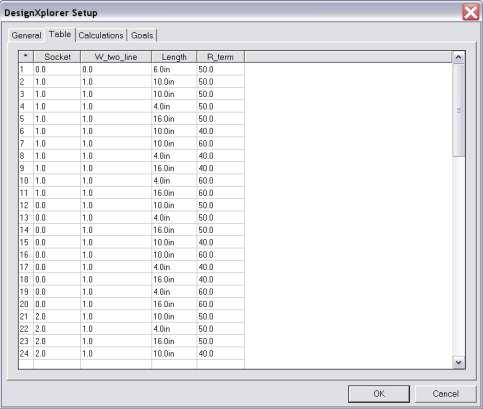
14 PCIe Channel Example DOE Setup 15 ANSYS, Inc. September 14,
 variables The Measure of fit provides a")
 = 0.")

15 Response Surfaces Visualize response surfaces in 3D or 2D plots (continuous, discreet, mixed) variables The Measure of fit provides a metric for evaluating the accuracy of the response surface model. 16 Eye Height Coefficient of Determination (R-Squared) = Eye Width Coefficient of Determination (R-Squared).= ANSYS, Inc. September 14, Provides a measure of how well future Outcomes will be predicted By the statistical model
16 Sensitivity Plots Which variables have the most impact on the output. Negative numbers show a decrease impact on output Positive numbers show an increase impact on output Sensitivity plots help us make the decision; which variable in my design offers the most impact changing my eye height or width. More importantly is shows up which inputs we may consider fixing thus narrowing the data set 17 ANSYS, Inc. September 14,


17 Optimization Min. EYE Height/Width 18 ANSYS, Inc. September 14,
18 Narrowing the field At this stage we know two valuable insights; which variable set yields the worst case eye which of those variables don t contribute much to this case. Additional judgment also comes into play here for example: Manufacturability Cost We narrow the field of variables and re-run the DOE for improved accuracy. Minimized to just the Package, Board, and Card T-line lengths 19 ANSYS, Inc. September 14,

19 Sensitivities updated of second DOE Package Length board Length Change in relative significance 20 ANSYS, Inc. September 14,
20 Defect Rate Prediction (DPMO) If we cannot achieve an acceptable design on one or more of our output criteria we need to determine whether or not our design can meet a specific defect rate target in this case, 1000ppm. For this case we will leave the design in the worst case and see how it does in the six sigma analysis for DPMO (Defects Per Million Opportunities) or ppm ( parts per million) 21 ANSYS, Inc. September 14,


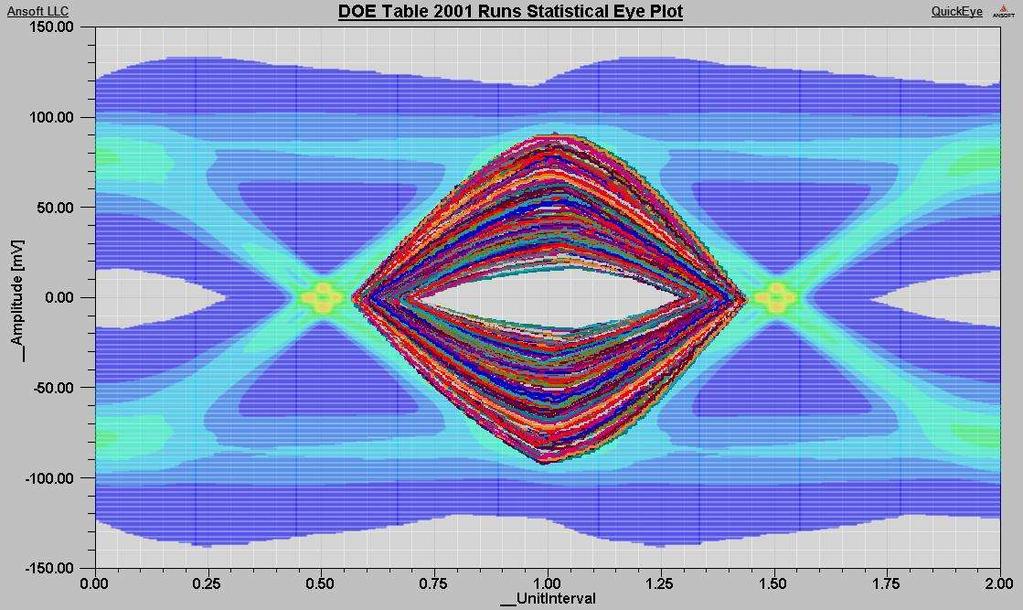
21 6-Sigma Distribution functions Plots showing the normal probability distribution and Cumulative distribution functions for Eye Width and Eye Height. 22 ANSYS, Inc. September 14,
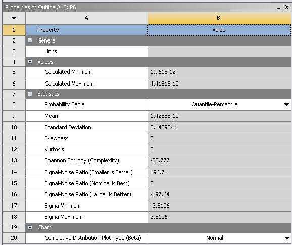
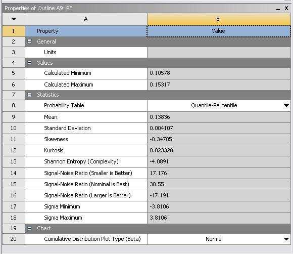
22 Distribution Characteristics 23 ANSYS, Inc. September 14,


23 DPMO Eye Height at worst case is with in the PCIe spec at 25mVPP Eye Width simulation shows possible violations of 0.3(UI) with a Sigma Level of With a Sigma Level at corresponding to 559 DPMO were within our 1000DPMO goal!! 24 ANSYS, Inc. September 14,
24 Summary Response Surface Modeling enables the designer to model and consider all aspects of a high speed channel design. optimized conditions and worst case scenarios are obtainable within the set of all possible design combinations within a realistic simulation timeframe. Using a cohesive tool set such as Designer SI and DesignXplorer improves simulation time, and reduces operator error. Designer Si as the circuit simulation tool directly linked to electromagnetic models yields the highest possible accuracy. Transient, statistical transient, peak distortion analysis, and equalization schemes are all inclusive within the Designer environments and can be part of the DOE, improves goodness of fit R^2 25 ANSYS, Inc. September 14,
25 Summary of tools Designer SI Circuit HFSS SOD DesignXplorer HPC pack 26 ANSYS, Inc. September 14,
Ansoft Designer with Nexxim. Statistical Eye Capabilities
 Ansoft Designer with Nexxim Statistical Eye Capabilities Problem Statement Load Generic 0.25um M odels Buffer PCIE Connector BYPASS Planar EM S S S TRL TRL TRL TRL TRL TRL Programmable W-Element SI Wave
Lecture 5: Dynamic Link
 Lecture 5: Dynamic Link 2015.0 Release ANSYS HFSS for Antenna Design 1 2015 ANSYS, Inc. Antenna System Co-Simulation Transmit/Receive (T/R) Module Block Diagram Antenna Element Replicate Times Power
End-to-End System-Level Simulations with Repeaters for PCIe Gen4: A How-To Guide
 DesignCon 2017 End-to-End System-Level Simulations with Repeaters for PCIe Gen4: A How-To Guide Yongyao Li, Huawei liyongyao@huawei.com Casey Morrison, Texas Instruments cmorrison@ti.com Fangyi Rao, Keysight
Ansys Designer RF Training Lecture 3: Nexxim Circuit Analysis for RF
 Ansys Designer RF Solutions for RF/Microwave Component and System Design 7. 0 Release Ansys Designer RF Training Lecture 3: Nexxim Circuit Analysis for RF Designer Overview Ansoft Designer Advanced Design
ANSYS CPS SOLUTION FOR SIGNAL AND POWER INTEGRITY
 ANSYS CPS SOLUTION FOR SIGNAL AND POWER INTEGRITY Rémy FERNANDES Lead Application Engineer ANSYS 1 2018 ANSYS, Inc. February 2, 2018 ANSYS ANSYS - Engineering simulation software leader Our industry reach
Authors: Feng Shi, Anders Ekholm, Zilwan Mahmod & David Zhang.
 A practical DOE Application in statistical SI analysis using IBIS & How can we make IBIS work beyond Best Case/Worst Case? Asian IBIS Summit November 9, 2015 Shanghai, China Authors: Feng Shi, Anders Ekholm,
How to anticipate Signal Integrity Issues: Improve my Channel Simulation by using Electromagnetic based model
 How to anticipate Signal Integrity Issues: Improve my Channel Simulation by using Electromagnetic based model HSD Strategic Intent Provide the industry s premier HSD EDA software. Integration of premier
Mini Modules Castellation Pin Layout Guidelines - For External Antenna
 User Guide Mini Modules Castellation Pin Layout Guidelines - For External Antenna Dcoument No: 0011-00-17-03-000 (Issue B) INTRODUCTION The MeshConnect EM35x Mini Modules (ZICM35xSP0-1C and ZICM35xSP2-1C)
PCB Routing Guidelines for Signal Integrity and Power Integrity
 PCB Routing Guidelines for Signal Integrity and Power Integrity Presentation by Chris Heard Orange County chapter meeting November 18, 2015 1 Agenda Insertion Loss 101 PCB Design Guidelines For SI Simulation
High-Performance Electronic Design: Predicting Electromagnetic Interference
 White Paper High-Performance Electronic Design: In designing electronics in today s highly competitive markets, meeting requirements for electromagnetic compatibility (EMC) presents a major risk factor,
Considerations in High-Speed High Performance Die-Package-Board Co-Design. Jenny Jiang Altera Packaging Department October 2014
 Considerations in High-Speed High Performance Die-Package-Board Co-Design Jenny Jiang Altera Packaging Department October 2014 Why Co-Design? Complex Multi-Layer BGA Package Horizontal and vertical design
Effect of Power Noise on Multi-Gigabit Serial Links
 Effect of Power Noise on Multi-Gigabit Serial Links Ken Willis (kwillis@sigrity.com) Kumar Keshavan (ckumar@sigrity.com) Jack Lin (jackwclin@sigrity.com) Tariq Abou-Jeyab (tariqa@sigrity.com) Sigrity Inc.,
Modeling Physical PCB Effects 5&
 Abstract Getting logical designs to meet specifications is the first step in creating a manufacturable design. Getting the physical design to work is the next step. The physical effects of PCB materials,
High Speed Characterization Report
 PCIEC-XXX-XXXX-EC-EM-P Mated with: PCIE-XXX-02-X-D-TH Description: 1.00 mm PCI Express Internal Cable Assembly, 30 AWG Twinax Ribbon Cable Samtec, Inc. 2005 All Rights Reserved Table of Contents Cable
Myoung Joon Choi, Vishram S. Pandit Intel Corp.
 Myoung Joon Choi, Vishram S. Pandit Intel Corp. IBIS Summit at DesignCon 2010 Acknowledgements: Woong Hwan Ryu, Joe Salmon Copyright 2010, Intel Corporation. All rights reserved. Need for SI/PI Co-analysis
Relationship Between Signal Integrity and EMC
 Relationship Between Signal Integrity and EMC Presented by Hasnain Syed Solectron USA, Inc. RTP, North Carolina Email: HasnainSyed@solectron.com 06/05/2007 Hasnain Syed 1 What is Signal Integrity (SI)?
Matched Terminated Stub for VIA Higher Technology Bandwidth Transmission. in Line Cards and Back Planes. Printed Circuit Board Operations
 Matched Terminated Stub VIA Technology Matched Terminated Stub for VIA Higher Technology Bandwidth Transmission for Higher Bandwidth Transmission in Line Cards and Back Planes. in Line Cards and Back Planes.
25Gb/s Ethernet Channel Design in Context:
 25Gb/s Ethernet Channel Design in Context: Channel Operating Margin (COM) Brandon Gore April 22 nd 2016 Backplane and Copper Cable Ethernet Interconnect Channel Compliance before IEEE 802.3bj What is COM?
1 Introduction External Component Requirements AC Coupling Capacitors on high speed lanes... 2
 PI3TB212 PI3TB212 Thunderbolt Application Information Table of Contents 1 Introduction... 2 2 External Component Requirements... 2 2.1 AC Coupling Capacitors on high speed lanes... 2 2.2 Pull-down Resistor
PI3DPX1207B Layout Guideline. Table of Contents. 1 Layout Design Guideline Power and GROUND High-speed Signal Routing...
 PI3DPX1207B Layout Guideline Table of Contents 1 Layout Design Guideline... 2 1.1 Power and GROUND... 2 1.2 High-speed Signal Routing... 3 2 PI3DPX1207B EVB layout... 8 3 Related Reference... 8 Page 1
Chip Package - PC Board Co-Design: Applying a Chip Power Model in System Power Integrity Analysis
 Chip Package - PC Board Co-Design: Applying a Chip Power Model in System Power Integrity Analysis Authors: Rick Brooks, Cisco, ricbrook@cisco.com Jane Lim, Cisco, honglim@cisco.com Udupi Harisharan, Cisco,
Engineering the Power Delivery Network
 C HAPTER 1 Engineering the Power Delivery Network 1.1 What Is the Power Delivery Network (PDN) and Why Should I Care? The power delivery network consists of all the interconnects in the power supply path
DP Array DPAM/DPAF Final Inch Designs in Serial ATA Generation 1 Applications 10mm Stack Height. REVISION DATE: January 11, 2005
 Application Note DP Array DPAM/DPAF Final Inch Designs in Serial ATA Generation 1 Applications 10mm Stack Height REVISION DATE: January 11, 2005 Copyrights and Trademarks Copyright 2005 Samtec, Inc. Developed
High Speed Characterization Report
 ECDP-16-XX-L1-L2-2-2 Mated with: HSEC8-125-XX-XX-DV-X-XX Description: High-Speed 85Ω Differential Edge Card Cable Assembly, 30 AWG ACCELERATE TM Twinax Cable Samtec, Inc. 2005 All Rights Reserved Table
The Challenges of Differential Bus Design
 The Challenges of Differential Bus Design February 20, 2002 presented by: Arthur Fraser TechKnowledge Page 1 Introduction Background Historically, differential interconnects were often twisted wire pairs
Q2 QMS-DP/QFS-DP Series 11 mm Stack Height Final Inch Designs in Serial ATA Generation 1 Applications. Revision Date: February 22, 2005
 Q2 QMS-DP/QFS-DP Series 11 mm Stack Height Final Inch Designs in Serial ATA Generation 1 Applications Revision Date: February 22, 2005 Copyrights and Trademarks Copyright 2005 Samtec, Inc. Developed in
RiseUp RU8-DP-DV Series 19mm Stack Height Final Inch Designs in Serial ATA Generation 1 Applications. Revision Date: March 18, 2005
 RiseUp RU8-DP-DV Series 19mm Stack Height Final Inch Designs in Serial ATA Generation 1 Applications Revision Date: March 18, 2005 Copyrights and Trademarks Copyright 2005 Samtec, Inc. Developed in conjunction
QPairs QTE-DP/QSE-DP Final Inch Designs in Serial ATA Generation 1 Applications 5mm Stack Height. REVISION DATE: January 12, 2005
 Application Note QPairs QTE-DP/QSE-DP Final Inch Designs in Serial ATA Generation 1 Applications 5mm Stack Height REVISION DATE: January 12, 2005 Copyrights and Trademarks Copyright 2005 Samtec, Inc. Developed
High Speed Characterization Report
 PCRF-064-XXXX-EC-SMA-P-1 Mated with: PCIE-XXX-02-X-D-TH Description: PCI Express Cable Assembly, Low Loss Microwave Cable Samtec, Inc. 2005 All Rights Reserved Table of Contents Cable Assembly Overview...
Validation Report Comparison of Eye Patterns Generated By Synopsys HSPICE and the Agilent PLTS
 Comparison of Eye Patterns Generated By Synopsys HSPICE and the Agilent PLTS Using: Final Inch Test/Eval Kit, Differential Pair - No Grounds Configuration, QTE-DP/QSE-DP, 5mm Stack Height (P/N FIK-QxE-04-01)
Evaluation of Package Properties for RF BJTs
 Application Note Evaluation of Package Properties for RF BJTs Overview EDA simulation software streamlines the development of digital and analog circuits from definition of concept and estimation of required
High Speed Characterization Report
 SSW-1XX-22-X-D-VS Mates with TSM-1XX-1-X-DV-X Description: Surface Mount Terminal Strip,.1 [2.54mm] Pitch, 13.59mm (.535 ) Stack Height Samtec, Inc. 25 All Rights Reserved Table of Contents Connector Overview...
High Speed Characterization Report
 ESCA-XX-XX-XX.XX-1-3 Mated with: SEAF8-XX-05.0-X-XX-2-K SEAM8-XX-S02.0-X-XX-2-K Description: 0.80 mm SEARAY High-Speed/High-Density Array Cable Assembly, 34 AWG Samtec, Inc. 2005 All Rights Reserved Table
Appendix. RF Transient Simulator. Page 1
 Appendix RF Transient Simulator Page 1 RF Transient/Convolution Simulation This simulator can be used to solve problems associated with circuit simulation, when the signal and waveforms involved are modulated
High Speed Characterization Report
 HLCD-20-XX-TD-BD-2 Mated with: LSHM-120-XX.X-X-DV-A Description: 0.50 mm Razor Beam High Speed Hermaphroditic Coax Cable Assembly Samtec, Inc. 2005 All Rights Reserved Table of Contents Cable Assembly
Power integrity is more than decoupling capacitors The Power Integrity Ecosystem. Keysight HSD Seminar Mastering SI & PI Design
 Power integrity is more than decoupling capacitors The Power Integrity Ecosystem Keysight HSD Seminar Mastering SI & PI Design Signal Integrity Power Integrity SI and PI Eco-System Keysight Technologies
Signal Integrity Modeling and Simulation for IC/Package Co-Design
 Signal Integrity Modeling and Simulation for IC/Package Co-Design Ching-Chao Huang Optimal Corp. October 24, 2004 Why IC and package co-design? The same IC in different packages may not work Package is
March 6-9, 2016 Hilton Phoenix / Mesa Hotel Mesa, Arizona Archive- Session 4
 Proceedings Archive March 6-9, 2016 Hilton Phoenix / Mesa Hotel Mesa, Arizona Archive- Session 4 2016 BiTS Workshop Image: Stiop / Dollarphotoclub Proceedings Archive Presentation / Copyright Notice The
2005 Modelithics Inc.
 Precision Measurements and Models You Trust Modelithics, Inc. Solutions for RF Board and Module Designers Introduction Modelithics delivers products and services to serve one goal accelerating RF/microwave
CROSSTALK DUE TO PERIODIC PLANE CUTOUTS. Jason R. Miller, Gustavo Blando, Istvan Novak Sun Microsystems
 CROSSTALK DUE TO PERIODIC PLANE CUTOUTS Jason R. Miller, Gustavo Blando, Istvan Novak Sun Microsystems 1 Outline 1 Introduction 2 Crosstalk Theory 3 Measurement 4 Simulation correlation 5 Parameterized
The wireless industry
 From May 2007 High Frequency Electronics Copyright Summit Technical Media, LLC RF SiP Design Verification Flow with Quadruple LO Down Converter SiP By HeeSoo Lee and Dean Nicholson Agilent Technologies
High Speed Characterization Report
 QTH-030-01-L-D-A Mates with QSH-030-01-L-D-A Description: High Speed Ground Plane Header Board-to-Board, 0.5mm (.0197 ) Pitch, 5mm (.1969 ) Stack Height Samtec, Inc. 2005 All Rights Reserved Table of Contents
PCB insertion loss test system
 PCB insertion loss test system Accura t e m e a s u re m e n t o f transmission line i n s e r t i o n l o s s f o r multi-gh z P C B f a b r i c a t i o n Atlas 2010 polarinstruments.com Ensures accurate
Characterization Methodology for High Density Microwave Fixtures. Dr. Brock J. LaMeres, Montana State University
 DesignCon 2008 Characterization Methodology for High Density Microwave Fixtures Dr. Brock J. LaMeres, Montana State University lameres@ece.montana.edu Brent Holcombe, Probing Technology, Inc brent.holcombe@probingtechnology.com
Backchannel Modeling and Simulation Using Recent Enhancements to the IBIS Standard
 Backchannel Modeling and Simulation Using Recent Enhancements to the IBIS Standard By Ken Willis, Product Engineering Architect; Ambrish Varma, Senior Principal Software Engineer; Dr. Kumar Keshavan, Senior
IBIS-AMI Terminology Overview
 IBIS-AMI Terminology Overview Walter Katz, SiSoft wkatz@sisoft.com Mike Steinberger, SiSoft msteinb@sisoft.com Todd Westerhoff, SiSoft twesterh@sisoft.com DAC 2009 IBIS Summit San Francisco, CA July 28,
To learn statistical bit-error-rate (BER) simulation, BER link noise budgeting and using ADS to model high speed I/O link circuits
 simulation, BER link noise budgeting and using ADS to model high speed I/O link circuits") 1 ECEN 720 High-Speed Links: Circuits and Systems Lab6 Link Modeling with ADS Objective To learn statistical bit-error-rate (BER) simulation, BER link noise budgeting and using ADS to model high speed
1 ECEN 720 High-Speed Links: Circuits and Systems Lab6 Link Modeling with ADS Objective To learn statistical bit-error-rate (BER) simulation, BER link noise budgeting and using ADS to model high speed
EDI CON USA Addressing DDR5 design challenges with IBIS-AMI modeling techniques. Todd Westerhoff, SiSoft Doug Burns, SiSoft Eric Brock, SiSoft
 EDI CON USA 2017 Addressing DDR5 design challenges with IBIS-AMI modeling techniques Todd Westerhoff, SiSoft Doug Burns, SiSoft Eric Brock, SiSoft This page intentionally blank to support double-sided
AN 766: Intel Stratix 10 Devices, High Speed Signal Interface Layout Design Guideline
 AN 766: Intel Stratix 10 Devices, High Speed Signal Interface Layout Subscribe Latest document on the web: PDF HTML Contents Contents Intel Stratix 10 Devices, High Speed Signal Interface Layout... 3 Intel
Logic Analyzer Probing Techniques for High-Speed Digital Systems
 DesignCon 2003 High-Performance System Design Conference Logic Analyzer Probing Techniques for High-Speed Digital Systems Brock J. LaMeres Agilent Technologies Abstract Digital systems are turning out
Comparison of Time Domain and Statistical IBIS-AMI Analyses Mike LaBonte SiSoft
 Comparison of Time Domain and Statistical IBIS-AMI Analyses Mike LaBonte SiSoft Asian IBIS Summit 2017 Taipei, ROC November 15, 2017 9 Combinations of TX and RX Model Types AMI file has: GetWave_Exists
Comparison of Time Domain and Statistical IBIS-AMI Analyses
 Comparison of Time Domain and Statistical IBIS-AMI Analyses Mike LaBonte SiSoft Asian IBIS Summit 2017 Shanghai, PRC November 13, 2017 9 Combinations of TX and RX Model Types AMI file has: GetWave_Exists
High Speed Characterization Report
 ERCD_020_XX_TTR_TED_1_D Mated with: ERF8-020-05.0-S-DV-L Description: 0.8mm Edge Rate High Speed Coax Cable Assembly Samtec, Inc. 2005 All Rights Reserved Table of Contents Cable Assembly Overview... 1
Low Noise Amplifier Design Methodology Summary By Ambarish Roy, Skyworks Solutions, Inc.
 February 2014 Low Noise Amplifier Design Methodology Summary By Ambarish Roy, Skyworks Solutions, Inc. Low Noise Amplifiers (LNAs) amplify weak signals received by the antenna in communication systems.
Bridging the Measurement and Simulation Gap Sarah Boen Marketing Manager Tektronix
 Bridging the Measurement and Simulation Gap Sarah Boen Marketing Manager Tektronix 1 Agenda Synergy between simulation and lab based measurements IBIS-AMI overview Simulation and measurement correlation
Fundamentals of RF Design RF Back to Basics 2015
 Fundamentals of RF Design 2015 Updated January 1, 2015 Keysight EEsof EDA Objectives Review Simulation Types Understand fundamentals on S-Parameter Simulation Additional Linear and Non-Linear Simulators
Predicting and Controlling Common Mode Noise from High Speed Differential Signals
 Predicting and Controlling Common Mode Noise from High Speed Differential Signals Bruce Archambeault, Ph.D. IEEE Fellow, inarte Certified Master EMC Design Engineer, Missouri University of Science & Technology
Electrical Characteristics Analysis and Comparison between Through Silicon Via(TSV) and Through Glass Via(TGV)
 and Through Glass Via(TGV)") Electrical Characteristics Analysis and Comparison between Through Silicon Via(TSV) and Through Glass Via(TGV) Jihye Kim, Insu Hwang, Youngwoo Kim, Heegon Kim and Joungho Kim Department of Electrical Engineering
Electrical Characteristics Analysis and Comparison between Through Silicon Via(TSV) and Through Glass Via(TGV) Jihye Kim, Insu Hwang, Youngwoo Kim, Heegon Kim and Joungho Kim Department of Electrical Engineering
Chapter 12: Electronic Circuit Simulation and Layout Software
 Chapter 12: Electronic Circuit Simulation and Layout Software In this chapter, we introduce the use of analog circuit simulation software and circuit layout software. I. Introduction So far we have designed
SERDES High-Speed I/O Implementation
 SERDES High-Speed I/O Implementation FTF-NET-F0141 Jon Burnett Digital Networking Hardware A R P. 2 0 1 4 External Use Overview SerDes Background TX Equalization RX Equalization TX/RX Equalization optimization
EMI. Chris Herrick. Applications Engineer
 Fundamentals of EMI Chris Herrick Ansoft Applications Engineer Three Basic Elements of EMC Conduction Coupling process EMI source Emission Space & Field Conductive Capacitive Inductive Radiative Low, Middle
IBIS-AMI Modeling Recommendations European IBIS Summit 2010
 IBIS-AMI Modeling Recommendations European IBIS Summit 2010 May 12, 2010 Hildesheim, Germany Kumar Keshavan Ken Willis Presented by Srdjan Djordjevic Agenda When is AMI required? IBIS-AMI key concepts
06-011r0 Towards a SAS-2 Physical Layer Specification. Kevin Witt 11/30/2005
 06-011r0 Towards a SAS-2 Physical Layer Specification Kevin Witt 11/30/2005 Physical Layer Working Group Goal Draft a Specification which will: 1. Meet the System Designers application requirements, 2.
Electrical Test Vehicle for High Density Fan-Out WLP for Mobile Application. Institute of Microelectronics 22 April 2014
 Electrical Test Vehicle for High Density Fan-Out WLP for Mobile Application Institute of Microelectronics 22 April 2014 Challenges for HD Fan-Out Electrical Design 15-20 mm 7 mm 6 mm SI/PI with multilayer
Introduction to ANSYS SIwave
 Workshop 8: DC 14.5 Release Introduction to ANSYS SIwave SIwave DC Analysis DC Voltage (DCIR) Drop Across a PWB This DCIR example is intended to show you how to simulate the voltage drop across a power
The Practical Limitations of S Parameter Measurements and the Impact on Time- Domain Simulations of High Speed Interconnects
 The Practical Limitations of S Parameter Measurements and the Impact on Time- Domain Simulations of High Speed Interconnects Dennis Poulin Anritsu Company Slide 1 Outline PSU Signal Integrity Symposium
Controlled Impedance Line Designer
 Heidi Barnes WW HSD Application Engineer Controlled Impedance Line Designer Stephen Slater HSD Product Manager EDA Simulation Tools for Power Integrity Agenda 1. Designing a channel for a desired impedance
Case Study Package Design & SI/PI analysis
 Caliber Interconnect Solutions Design for perfection Case Study Package Design & SI/PI analysis Caliber Interconnect Solutions (Pvt) Ltd No 6,1 st Street Gandhi Nagar, Kavundampalayam, Coimbatore-30. Tamil
DL-150 The Ten Habits of Highly Successful Designers. or Design for Speed: A Designer s Survival Guide to Signal Integrity
 Slide -1 Ten Habits of Highly Successful Board Designers or Design for Speed: A Designer s Survival Guide to Signal Integrity with Dr. Eric Bogatin, Signal Integrity Evangelist, Bogatin Enterprises, www.bethesignal.com
W2360EP/ET SIPro Signal Integrity EM Analysis W2359EP/ET PIPro Power Integrity EM Analysis
 Keysight Technologies Advanced Design System (ADS) W2360EP/ET SIPro Signal Integrity EM Analysis W2359EP/ET PIPro Power Integrity EM Analysis Data Sheet Composite EM technology delivers high-accuracy and
Electromagnetic Simulation of Antennas Installed Inside Vehicles An Automotive EMC Approach Markus Kopp Product Manager, Electronics
 Electromagnetic Simulation of Antennas Installed Inside Vehicles An Automotive EMC Approach Markus Kopp Product Manager, Electronics 1 Automotive Antenna Systems and Automotive EMC Recent technology implementations
Highly Accurate and Robust Automotive Radar System Design. Markus Kopp Lead Application Specialist ANSYS Inc.
 Highly Accurate and Robust Automotive Radar System Design Markus Kopp Lead Application Specialist ANSYS Inc. Introduction This presentation is an overview of a proposed design methodology for automotive
DesignCon 2010 Predicting BER with IBIS-AMI: experiences correlating SerDes simulations and measurement
 DesignCon 2010 Predicting BER with IBIS-AMI: experiences correlating SerDes simulations and measurement Todd Westerhoff, Signal Integrity Software, Inc. twesterh@sisoft.com Adge Hawes, IBM adge@uk.ibm.com
3D IC-Package-Board Co-analysis using 3D EM Simulation for Mobile Applications
 3D IC-Package-Board Co-analysis using 3D EM Simulation for Mobile Applications Darryl Kostka, CST of America Taigon Song and Sung Kyu Lim, Georgia Institute of Technology Outline Introduction TSV Array
Automotive PCB SI and PI analysis
 Automotive PCB SI and PI analysis SI PI Analysis Signal Integrity S-Parameter Timing analysis Eye diagram Power Integrity Loop / Partial inductance DC IR-Drop AC PDN Impedance Power Aware SI Signal Integrity
Realize Your Product Promise. Maxwell
 Realize Your Product Promise Maxwell DC permanent magnet motor solved by Maxwell with ANSYS RMxprt Build reliability and efficiency into your electromagnetic and electromechanical designs with ANSYS Maxwell.
Low-Cost PCB Design 1
 Low-Cost PCB Design 1 PCB design parameters Defining PCB design parameters begins with understanding: End product features, uses, environment, and lifetime goals PCB performance, manufacturing, and yield
BSW MHz-6000MHz High Linearity Reflective SPDT RF switch. Product Description. Package Type. Device Features - Common.
 Product Description The BSW6321 is a reflective SPDT RF switch that can be used in high power and good performance WiMAX 802.16, WLAN 802.11 a/b/g/n/ac/ax and DOCSIS 3.0/3.1 applications. This device is
Christian Römelsberger (CADFEM GmbH) Ivan Vukosav (Yazaki)
 Ivan Vukosav (Yazaki)") Titelmasterformat TDR of a Connector durch with Klicken wiring Harness bearbeiten Christian Römelsberger (CADFEM GmbH) Ivan Vukosav (Yazaki) 1 Products Service Knowledge Full scale CAE solution based on
Titelmasterformat TDR of a Connector durch with Klicken wiring Harness bearbeiten Christian Römelsberger (CADFEM GmbH) Ivan Vukosav (Yazaki) 1 Products Service Knowledge Full scale CAE solution based on
DL-150 The Ten Habits of Highly Successful Designers. or Design for Speed: A Designer s Survival Guide to Signal Integrity
 Slide -1 Ten Habits of Highly Successful Board Designers or Design for Speed: A Designer s Survival Guide to Signal Integrity with Dr. Eric Bogatin, Signal Integrity Evangelist, Bogatin Enterprises, www.bethesignal.com
Caliber Interconnect Solutions
 Caliber Interconnect Solutions Design for perfection CASE STUDY DBFSP card and Optical card Transceivers Channels (through Backplane) Pre-Layout SI Report Caliber Interconnect Solutions (Pvt) Ltd No 6,1
TABLE OF CONTENTS. Sliver Cable Assemblies. TE Connectivity Technical Datasheet
 TABLE OF CONTENTS Introduction... 2 Description... 2 Features and Benefits... 2 Product Applications... 2 Industry Standards... 2 Technical Documents... 2 Part Numbers... 3 Table 1. Part Number Selection
Reliable World Class Insights Your Silicon Valley Partner in Simulation ANSYS Sales, Consulting, Training & Support
 www.ozeninc.com info@ozeninc.com (408) 732 4665 1210 E Arques Ave St 207 Sunnyvale, CA 94085 Reliable World Class Insights Your Silicon Valley Partner in Simulation ANSYS Sales, Consulting, Training &
Thank you for downloading one of our ANSYS whitepapers we hope you enjoy it.
 Thank you! Thank you for downloading one of our ANSYS whitepapers we hope you enjoy it. Have questions? Need more information? Please don t hesitate to contact us! We have plenty more where this came from.
Aries Center probe CSP socket Cycling test
 Aries Center probe CSP socket Cycling test RF Measurement Results prepared by Gert Hohenwarter 10/27/04 1 Table of Contents TABLE OF CONTENTS... 2 OBJECTIVE... 3 METHODOLOGY... 3 Test procedures... 5 Setup...
Research in Support of the Die / Package Interface
 Research in Support of the Die / Package Interface Introduction As the microelectronics industry continues to scale down CMOS in accordance with Moore s Law and the ITRS roadmap, the minimum feature size
Aries QFP microstrip socket
 Aries QFP microstrip socket Measurement and Model Results prepared by Gert Hohenwarter 2/18/05 1 Table of Contents Table of Contents... 2 OBJECTIVE... 3 METHODOLOGY... 3 Test procedures... 4 Setup... 4
Practical Design Considerations for Dense, High-Speed, Differential Stripline PCB Routing Related to Bends, Meanders and Jog-outs
 Practical Design Considerations for Dense, High-Speed, Differential Stripline PCB Routing Related to Bends, Meanders and Jog-outs AUTHORS Michael J. Degerstrom, Mayo Clinic degerstrom.michael@mayo.edu
Practical Limitations of State of the Art Passive Printed Circuit Board Power Delivery Networks for High Performance Compute Systems
 Practical Limitations of State of the Art Passive Printed Circuit Board Power Delivery Networks for High Performance Compute Systems Presented by Chad Smutzer Mayo Clinic Special Purpose Processor Development
Aries Kapton CSP socket
 Aries Kapton CSP socket Measurement and Model Results prepared by Gert Hohenwarter 5/19/04 1 Table of Contents Table of Contents... 2 OBJECTIVE... 3 METHODOLOGY... 3 Test procedures... 4 Setup... 4 MEASUREMENTS...
High Speed Characterization Report
 HDLSP-035-2.00 Mated with: HDI6-035-01-RA-TR/HDC-035-01 Description: High Density/High Speed IO Cable Assembly Samtec, Inc. 2005 All Rights Reserved Table of Contents Introduction...1 Product Description...1
Enabling Parallel Testing at Sort for High Power Products
 Enabling Parallel Testing at Sort for High Power Products Abdel Abdelrahman Tim Swettlen 2200 Mission College Blvd. M/S SC2-07 Santa Clara, CA 94536 Abdel.Abdelrahman@intel.com Tim.Swettlen@intel.com Agenda
Data Sheet. ACMD-7612 Miniature UMTS Band I Duplexer. Features. Description. Specifications. Applications. Functional Block Diagram
 ACMD-7612 Miniature UMTS Band I Duplexer Data Sheet Description The Avago ACMD-7612 is a miniature duplexer designed for use in UMTS Band I handsets. Maximum Insertion Loss in the channel is only 1.5 db,
Amphenol AssembleTech. Contents. Mini Cool Edge IO (MCIO) Cable Assemblies. Amphenol AssembleTech Technical Datasheet
 Cable Assemblies. Amphenol AssembleTech Technical Datasheet") Contents Introduction........ 2 Description Features and Benefits Applications Industry Standards Technical Documents Part Numbers.......3 Table 1. Cable Connector Part Number Selection Guide Product Specifications........
Contents Introduction........ 2 Description Features and Benefits Applications Industry Standards Technical Documents Part Numbers.......3 Table 1. Cable Connector Part Number Selection Guide Product Specifications........
Anaren 0805 (B0809J50ATI) balun optimized for Texas Instruments CC1100/CC1101 Transceiver
 balun optimized for Texas Instruments CC1100/CC1101 Transceiver") (ANN-2005) Rev B Page 1 of 13 Anaren 0805 (B0809J50ATI) balun optimized for Texas Instruments CC1100/CC1101 Transceiver Trong N Duong RF Co-Op Nithya R Subramanian RF Engineer Introduction The tradeoff
(ANN-2005) Rev B Page 1 of 13 Anaren 0805 (B0809J50ATI) balun optimized for Texas Instruments CC1100/CC1101 Transceiver Trong N Duong RF Co-Op Nithya R Subramanian RF Engineer Introduction The tradeoff
Validation & Analysis of Complex Serial Bus Link Models
 Validation & Analysis of Complex Serial Bus Link Models Version 1.0 John Pickerd, Tektronix, Inc John.J.Pickerd@Tek.com 503-627-5122 Kan Tan, Tektronix, Inc Kan.Tan@Tektronix.com 503-627-2049 Abstract
Keysight Technologies Signal Integrity Tips and Techniques Using TDR, VNA and Modeling
 Keysight Technologies Signal Integrity Tips and Techniques Using, VNA and Modeling Article Reprint This article first appeared in the March 216 edition of Microwave Journal. Reprinted with kind permission
80GHz Notch Filter Design
 DIGITAL PRODUCTIVITY FLAGSHIP 80GHz Notch Filter Design Mark De Alwis 10 June 2015 ii 80GHz Notch Filter Design Important disclaimer CSIRO advises that the information contained in this publication comprises
PI3PCIE2612-B High Bandwidth, 6-Differential Channel 1:2 DP/PCIe Gen2 Display Mux, BTX Pinout
 Features 6 Differential Channel, 1 to 2 demux that will support 5.0Gbps PCIexpress Gen2 signals on one path, and DP 1.1 signals on the second path Insertion Loss for high speed channels @ 2.0 Gbps: -2.0dB
System Coupling 14.0 Twoway FSI with ANSYS FLUENT and ANSYS Mechanical
 System Coupling 14.0 Twoway FSI with ANSYS FLUENT and ANSYS Mechanical ANSYS Regional Conference 1 Fluid-Structure Interaction Applications Floating thin film Wind Turbine Mitral valve 2 Fluid-structure