Why do we need to study Signal Integrity, Power Integrity and EMI ALL-AT-ONCE?
|
|
|
- Giles Knight
- 6 years ago
- Views:
Transcription
1 Why do we need to study Signal Integrity, Power Integrity and EMI ALL-AT-ONCE? Hany Fahmy Riccardo Giacometti Cédric Pujol EMI HSD Signal Integrity Power Integrity

2 An Example of Dramatic increase in HSD Systems A look at Apple Macbook pro USB Gb/s HDMI 5 Gb/s DVI 8 Gb/s DP 8.6 Gb/s PCIe 5 Gb/s SATA 3 Gb/s DDR Gb/s Increased Density High-speed everywhere Pressure to Reduce cost
3 Typical High Speed Digital Challenges Impedance Mismatch: Line-width changes, Vias, Serpentines, Connectors, Cables Manufacturing tolerances for PCBs & Packages: effective dielectric constant, surface-roughness variations Tx output-impedance, Rx input-impedance vs. line impedance Crosstalk Noise Electromagnetic coupling between signal lines Trace-to-Trace crosstalk, Via-to-Via coupling, Digital/RF coupling Power/Ground Noise Tight requirements on PDN impedance as supply voltages decrease and currents increase to provide clean power to FPGA/ASICs Imperfect power/ground delivery system results in Simultaneous Switching Output (SSO) noise to propagate through the PDN EMI/EMC Performance Most of the above effects produce EM radiation Ideal waveform at the receiving gate. Real waveform at the receiving gate.
4 High-Speed Digital PCB Analysis/Verification Methodology Pre-layout Signal Integrity Analysis Post-layout Signal Integrity Verification Pre-layout Power Integrity Analysis Post-layout Power Integrity Verification EMI/EMC Analysis EMI HSD Signal Integrity Power Integrity


5 EMI HSD Signal Integrity Power Integrity Why do we need to study SI, PI and EMI all at once? SIGNAL INTEGRITY ANALYSIS
6 Signal Degradation due to non-ideal channel Low pass filter characteristic of transmission line (attenuates high frequency component in a signal which results in smearing out sharp edges) Radiation, dispersion, resonance, and frequency dependent losses of transmission line degrades wave shape Interference caused by cross talk (coupling between adjacent transmission lines) and radiations degrades wave shape Impedance mismatch due to transmission line discontinuities High frequency parasitics, delays, and asymmetric transmission paths Through Hole Vias Basic Microwave problem
7 Signal Integrity Analysis in ADS Pre-layout SI analysis Choice of stack-up, components, net width and spacing, terminations After placement, detailed analysis of critical nets including crosstalk, via effects, connector effects etc. Derive layout routing constraints Post-layout SI analysis Import board layout from Allegro (DFI link), Expedition, Boardstation etc. (ODB++) Complete EM analysis Verification of critical nets
8 Challenges in Pre-layout Design Space Exploration Multi-dimensional design space: Tx, channel, Rx Optimization goal is an extremely low BER Megabit eye diagrams required for this figure of merit Millions of simulation time steps BER at each point affect by: Jitter: ISI, DCD, PJ & RJ Channel impairments: attenuation, reflections, crosstalk Tx and Rx equalizers Some components specified in frequency-domain Beware of causality and passivity translation errors Traditional SPICE-like transient simulation requires tens of hours per megabit Optimization of Tx, channel, and Rx characteristics is impractical


9 Channel Simulator: Megabit Eye Diagram in One Minute per Point, not Ten Hours Integrate layout artwork into schematic


10 Eye Diagram and BER Comparison of Channel Simulator in Statistical and Bit-by-bit Modes ADS Channel Simulator Statistical Mode ADS Channel Simulator Bit-by-Bit Mode Timing Bathtub Voltage Bathtub ADS Channel Simulator (1 M bits) ADS Statistical Simulator ADS Channel Simulator (1 M bits) ADS Statistical Simulator
11 Example: Determine the Optimum Value of De-emphasis Optimum de-emphasis value: 5.6 db
12 Multilayer Transmission Lines Models in ADS Accurate models calculated by embedded 2D EM solver Fast simulation allows tuning/optimization Ideal for pre-layout analysis

13 Pre-Layout Case Study
14 Pre-layout Signal Integrity Analysis Signal Analysis to determine modeling BW Line analysis/optimization Width, intra-pair/inter-pair Spacing Impedance (TDR) Group delay (S-parameters) Crosstalk analysis/optimization Line-to-Line crosstalk Via-to-Via crosstalk Connectors, cables Margin verification using full-wave 3D EM models
15 Next Steps After Full Pre-layout Optimization Use optimized design rules, determined in pre-layout phase, as input to constraint editor in your enterprise constraint-based layout tool Cadence Allegro Mentor Expedition/Board station Zuken CR-5000 Post-layout predictive verification and fine tuning using ADS EM simulation on critical nets


16 Export Allegro Critical Nets to ADS Sandbox Select critical nets Select stackup layers Cookie-cut power and ground planes Create ports Export to.ads file ADS Layout sandbox Adjust layout EM sim results OK? No Yes Report fixes to physical designer who adjusts golden artwork in Allegro
17 Method Of Moments for PCB analysis Claim: MOM (Method of Moments) is the best full-wave technique for extracting S- parameters of Multi-layer PCBs and Packages Why? MOM does not need to discretize the Multi-layer Substrate if the substrate is homogeneous. MOM only discretizes areas with surface electric/magnetic currents MOM is faster than other techniques (FEM, MOL, FDTD) that require substrate discretization


18 MOM results correlate to VNA measurements S-parameter modeling of PCB & package interconnects Courtesy of Gigatest N1930B Physical Layer Test System (PLTS)

19 Need to model the following: Real cross-talk (not pre-layout) Signal layer transitions: L1-to-L3 is it same as L1-to-L5? Via stubs Serpentine routing for length-matching rules Stitching via impact (number & location)

20 8-Layer Package design: DDR3 memory channel SODIMM for memory controller

21 Impact of GND PTH stitching

22 Impact of PTH GND stitching

23 Impact of GND die-side Reduced GND die-side
24 Impact of stitching on IL Transmission from memory controller to GPU chip 0 via 8 vias 15 vias
25 What about the x-talk impact? Transmission from signal line to adjacent line 0 via 8 vias 15 vias


26 What about the jitter impact? Eye diagrams from 9 lines going from memory controller to GPU interface Initial grounding Final grounding
27 Advantages of ADS for HSD Not a collection of points tools. ADS is an integrated solution with: Accurate models refined over many years against measured data Causal S-parameter and multilayer transmission line models Jitter decomposition verified with Agilent EZ JIT Plus algorithm ADS Channel Simulator million bit per minute and statistical modes Pre-layout design space exploration Industry-leading ADS Transient Convolution for pre-layout final verification e.g. overnight run on non-linear components Design flow integration with artwork from enterprise board tools ADS Layout sandbox doesn t force you to learn 3-D MCAD manipulation Method of moments is the fastest and most accurate EM technique for trace-andvia geometries ADS Momentum G2 is the leading method of moments tool Predictive post-layout verification and fine tuning of artwork FEM for non trace-and-via geometries Balls, bond wires, dielectric bricks, connectors, etc.
28 EMI HSD Signal Integrity Power Integrity Why do we need to study SI, PI and EMI all at once? POWER INTEGRITY ANALYSIS
29 Simplified PDN Model
30 Important PI challenges that can affect design performance Analyze Power plane impedance vs. freq Find Power/Ground resonances Estimate Switching Noise spectrum Effective use of decoupling capacitors (On-die, On-PKG & On-PCB) Strategies that can improve power integrity: Low-impedance path from power supply to die Optimize/validate discrete decoupling capacitor network Analyze Via Transitions Avoid return path discontinuities define number and position of Stitching vias

31 Conceptual Origin of Simultaneous Switching Output (SSO) Noise On Chip Active loop I charge I discharge Switching lines Quiet data line V CC V SS L Bonding L Bonding Quiet loop GND Power Integrated Circuit Engineering Corporation common lead inductance What influences SSO Noise: Mutual inductance between the loops Number of SSOs di/dt
 = 0.25 Ohm 0.")
32 Simple PDN model Impedance seen by device 2.5V *(0.05) = 0.25 Ohm 0.5A
33 SSO Noise model
34 SSO Noise Simulation
 Simple MOCHA project[1] 1.")
35 Case Studies Large Area/Layers 3.Full DDR module ( Power/ Ground planes) Medium large 2.BGA package (DQ lines + Power/ Ground planes ) Simple MOCHA project[1] 1.Simple Power/Ground planes Frequency
36 Case1: Power Plane Impedance 10 cm 4 cm Example: PDN impedance Freq sweep 0-3 GHz RF mode Extracted power plane impedance Momentum 2011 MatrixSize: 15,042 Process Size: 1345 MB Elapsed Time: 31m56s Intel Core2 Quad ( 4 cores ) RAM: 4 GByte

37 PDN Analysis VRM Decoupling Caps Load
38 Case2: BGA Package (MOCHA project) 2.3cm 8 layers 1cm Example: BGA package VSS, VDD, DQ lines Freq sweep 0-10 GHz,200MHz step RF mode Using sheet conductor Momentum 2011 with bonding wire MatrixSize: Process Size: 4632 MB Elapsed Time: 2h51m6s Intel Xeon X5482 x 2 ( 8 cores ) RAM: 32 GByte MOCHA project [1]: Modeling and CHAracterization for SiP - Signal and Power Integrity Analysis
39 Case3: DDR Module 14.2cm 2.8 cm 8 layers Example: DDR module Power/Ground Freq sweep 0-3 GHz,200MHz step RF mode Using sheet conductor Momentum 2011 MatrixSize: 38,789 Process Size: MB Elapsed Time: 6h38m54s Intel Xeon X5530 x 2 ( 8 cores ) RAM: 64 GByte


40 mag(z) Signal and Power Integrity Simulation (SIPI) Wizard New in ADS2011 Guided EM simulation setup Enables net based selection and simulation Allows Port grouping/clustering Computes PDN impedance 0 Provide current distribution with SMD components freq, GHz
41 EMI HSD Signal Integrity Power Integrity Why do we need to study SI, PI and EMI all at once? EMI/EMC ANALYSIS

42 What are the different types of Radiated-Emission?


43 EMI SY S T E M B U D G E T Complexity of EMI problem Badly routed traces generate EMI High-speed connectors and cables amplify the EMI problems Connectors M I N I M I Z E IC, P K G, A N D P C B E M I TO R E D U C E O V E R A L L S Y S T E M E M I High-speed PCB High-speed IC * H-Field Measurement From EMscan of GPU Board
44 Limiting EMI Trace emission - Emission on a Digital Video Interface (DVI) example - Memory bus emission PCB Edge emission to due Power Delivery Network Cable emission


45 Problem Statement - DVI/HDMI are standard interfaces for video transmission - To minimize EMI, DVI/HDMI standards are using TMDS (Transition Minimized Differential Signaling ) technologies - TDMS operates at 10 times the pixel frequency (current DVI maximum for pixel frequency is 165 MHz)

46 Problem Statement (cont d) - In the context of a PC, DVI co-exists with other interfaces - On this example, the ethernet card/cables exhibit a TMDS signature emission at 770MHz


 R4N Suppressor band-aid")
47 Current solution Put on band-aid to stop the radiation. It is hardly optimal, does not always work, and costs lot of money Which one? Copper band-aid (well suited for E-coupling) R4N Suppressor band-aid (well suited for H-coupling)


48 What if we could simulate it! Using Momentum for 1 hour : 770 MHz Confirm max radiation at the bottom of PCB due to TMDS routing Max angle : 144/ uw in total power Antenna Gain is -48 db 5uW / steradian


49 With metal shielding Using Momentum for 1 hour : Metal shield and PCB ground with heat-sink screws 770 MHz Confirm max radiation at the bottom of PCB due to TMDS routing Max angle : 144/ uw in total power Worse! Antenna Gain is -47 db 6uW / steradian


50 With NEC/Tokin R4N shielding Using Momentum for 1 hour : R4N material placed at the bottom of the PCB 770 MHz Confirm max radiation at the bottom of PCB due to TMDS routing Max angle : 162/ uw in total power Antenna Gain is -51 db 2uW / steradian


51 Looking at it closer Original With R4N Connectors GPU 51

.")

52 And in the chamber? The measurement showed an improvement from 7.6 db to 8.2 db (0.6 db). Simulation predicted 3 db and so the correct trend. 52 Copyright 2009 Agilent Technologies, Inc.
53 Limiting EMI Trace emission - Emission on a Digital Video Interface (DVI) example - Memory bus emission PCB Edge emission to due Power Delivery Network Cable emission
54 4-layer PCB with Memory Emission problem GPU Problem: Investigate Emission problem at 1.25 of the memory clock frequency (1.623 GHz) Memory Notes: Address/Command Nets are routed on bottom-layer referencing Vddq power plane (due to lack of realestate)
 Simulations showing current-density plots and hot-spot regions on the PCB *Using Agilent")
55 EMI Simulation Methodology Step-1: Simulate and Visualize Current-density plot of the bottom of the card* Method-of-Moments (Momentum) Simulations showing current-density plots and hot-spot regions on the PCB *Using Agilent Momentum Field Solver

56 EMI Simulation Methodology, Cntd. Step-2: Isolate Problem Observe hot-spot area closely, and identify root-cause Root-cause: There is small λ/8 powerplane patch that is radiating like patch-antenna ~ 1cm Use Momentum UW with Antenna-Gain parameter to measure the merit of the PCB as non-intended antenna Develop EMI guidelines along with SI/PI Guidelines using Antenna-Gain Parameter to compare Layout guidelines
57 Limiting EMI Trace emission - Emission on a Digital Video Interface (DVI) example - Memory bus emission PCB Edge emission to due Power Delivery Network Cable emission
 Full wave EM simulation is often needed Time and memory")
58 EMI SY S T E M B U D G E T EMI Simulation challenges System level (source / coupling path) Full wave EM simulation is often needed Time and memory consuming
59 SSO Noise on the PCB Power Delivery Network Current VddQ pins of the GPU Drivers Channel Receivers SSO current is obtained by a combined simulation of the power delivery network model and the memory IO channel model

60 How does the SSO noise look like? fft ifft steady-state frequencies SSO noise is broadband Icc profiles are time-dependent FDTD is very well suited to handle SSO noise phenomena

61 8 cm Importing PCB layout of the Memory- Channel Stackup Signal Ground Signal VDD Ground VDD 11 cm board thickness: 1.57mm


62 PCB top layer : Including noise sources VSS notches Noise sources IC


63 PCB bottom layer : Decoupling caps decaps


64 Far field radiation of the SSO noise With Decaps Without Decaps With Decaps Without Decaps 0.5 GHz 1 GHz Reduction of 3-4 db

65 Current density at 500 MHz Without Decaps With Decaps
66 Simulation runtime FDTD has an inherent parallel nature, which makes it extremely well suited for GPU acceleration Acceleration Runtime CPU Over 1 week GPU acceleration (1 card) ~ 12 hours GPU acceleration (4 cards) ~ 1-2 hours Used 1.5 GB of RAM
67 Limiting EMI Trace emission - Emission on a Digital Video Interface (DVI) example - Memory bus emission PCB Edge emission to due Power Delivery Network Cable emission - Emission due to connectors - ESD protection


68 Board + Connector + Mate


69 Combining the board and the imported connectors Precise landing of connector fingers on board signal pad

70 Near-field radiation Simulated with EMPro FDTD solver Simulation time 2 hrs with 3-GPU cards Study if improved grounding & shielding of the connector improves EMI behavior

71 Improving grounding No copper tape Extra copper tape
72 Improving grounding : Far-field impact of CU-tape Reduction of 5 db for EMI emission in direction of chassis
73 Limiting EMI Trace emission - Emission on a Digital Video Interface (DVI) example - Memory bus emission PCB Edge emission to due Power Delivery Network Cable emission - Emission due to connectors - ESD protection


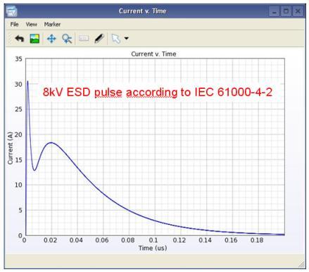
74 ESD protection Electrostatic discharges are meant to be temporary so only a transient-based engine can show their impact ~ 30 A / 8 kv Protective system 74 Copyright 2009 Agilent Technologies, Inc.

75 Location of ESD diodes
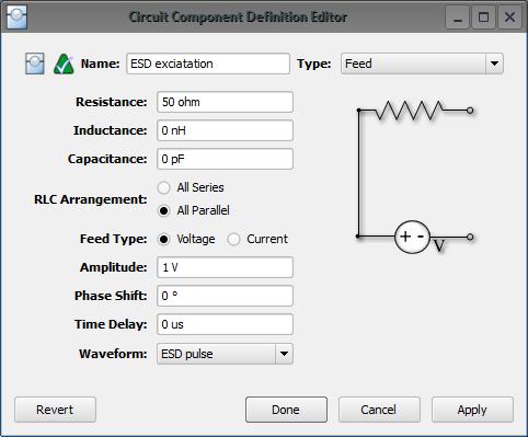
76 Excitation at connector side
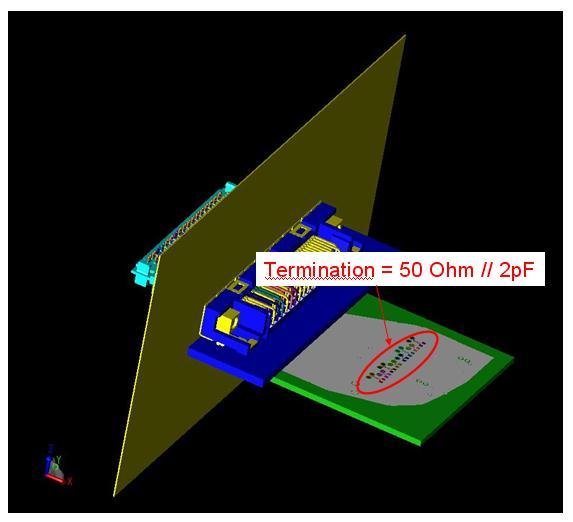
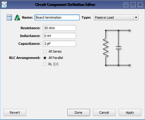
77 Termination at board Side

78 Voltages with no ESD Diode > 1.2 kv!! Traditionally, a rule of thumb is to place the ESD diodes close the connector for a better efficiency. Could we verify it on this case?


79 ESD output 30 V 50 V ESD diodes close to the connector ESD diodes close to the GPU
80 Simulation Time Acceleration Runtime CPU Over 1 week GPU acceleration (1 card) ~ 16 hours GPU acceleration (3 cards) ~ 5 hours
81 Conclusion No Single Methodology/Technique can do it all. Momentum is best Full-wave EM modeling for PCBs and Packages EMI HSD Power Integrity Signal Integrity FDTD is best for wide-band phenomena like SSO noise Emission, Conducted Emission and ESD especially if it is accelerated by GPU. FEM and FDTD for S-parameter modeling of PCB+Connector (Conducted- Emission FDTD, S-parameter model FEM) Having the 3 most-renowned EM technologies, Agilent is here to help you finding the adequate engine to solve your HSD problem
Introduction to EMI/EMC Challenges and Their Solution
 Introduction to EMI/EMC Challenges and Their Solution Dr. Hany Fahmy HSD Application Expert Agilent Technologies Davy Pissort, K.U. Leuven Charles Jackson, Nvidia Charlie Shu, Nvidia Chen Wang, Nvidia
How to anticipate Signal Integrity Issues: Improve my Channel Simulation by using Electromagnetic based model
 How to anticipate Signal Integrity Issues: Improve my Channel Simulation by using Electromagnetic based model HSD Strategic Intent Provide the industry s premier HSD EDA software. Integration of premier
Closing the loop part 1: Why use simulation tools for high speed signal channel design?
 Closing the loop part 1: Why use simulation tools for high speed signal channel design? Riccardo Giacometti Application Engineer Agilent EEsof EDA Page 1 High Speed Digital Design Flow Pre-Layout w/channel
Relationship Between Signal Integrity and EMC
 Relationship Between Signal Integrity and EMC Presented by Hasnain Syed Solectron USA, Inc. RTP, North Carolina Email: HasnainSyed@solectron.com 06/05/2007 Hasnain Syed 1 What is Signal Integrity (SI)?
ANSYS CPS SOLUTION FOR SIGNAL AND POWER INTEGRITY
 ANSYS CPS SOLUTION FOR SIGNAL AND POWER INTEGRITY Rémy FERNANDES Lead Application Engineer ANSYS 1 2018 ANSYS, Inc. February 2, 2018 ANSYS ANSYS - Engineering simulation software leader Our industry reach
Taking the Mystery out of Signal Integrity
 Slide - 1 Jan 2002 Taking the Mystery out of Signal Integrity Dr. Eric Bogatin, CTO, GigaTest Labs Signal Integrity Engineering and Training 134 S. Wolfe Rd Sunnyvale, CA 94086 408-524-2700 www.gigatest.com
EMC cases study. Antonio Ciccomancini Scogna, CST of America CST COMPUTER SIMULATION TECHNOLOGY
 EMC cases study Antonio Ciccomancini Scogna, CST of America antonio.ciccomancini@cst.com Introduction Legal Compliance with EMC Standards without compliance products can not be released to the market Failure
PDS Impact for DDR Low Cost Design
 PDS Impact for DDR3-1600 Low Cost Design Jack W.C. Lin Sr. AE Manager jackl@cadence.com Aug. g 13 2013 Cadence, OrCAD, Allegro, Sigrity and the Cadence logo are trademarks of Cadence Design Systems, Inc.
EMI. Chris Herrick. Applications Engineer
 Fundamentals of EMI Chris Herrick Ansoft Applications Engineer Three Basic Elements of EMC Conduction Coupling process EMI source Emission Space & Field Conductive Capacitive Inductive Radiative Low, Middle
Considerations in High-Speed High Performance Die-Package-Board Co-Design. Jenny Jiang Altera Packaging Department October 2014
 Considerations in High-Speed High Performance Die-Package-Board Co-Design Jenny Jiang Altera Packaging Department October 2014 Why Co-Design? Complex Multi-Layer BGA Package Horizontal and vertical design
Chapter 16 PCB Layout and Stackup
 Chapter 16 PCB Layout and Stackup Electromagnetic Compatibility Engineering by Henry W. Ott Foreword The PCB represents the physical implementation of the schematic. The proper design and layout of a printed
PCB Routing Guidelines for Signal Integrity and Power Integrity
 PCB Routing Guidelines for Signal Integrity and Power Integrity Presentation by Chris Heard Orange County chapter meeting November 18, 2015 1 Agenda Insertion Loss 101 PCB Design Guidelines For SI Simulation
Myoung Joon Choi, Vishram S. Pandit Intel Corp.
 Myoung Joon Choi, Vishram S. Pandit Intel Corp. IBIS Summit at DesignCon 2010 Acknowledgements: Woong Hwan Ryu, Joe Salmon Copyright 2010, Intel Corporation. All rights reserved. Need for SI/PI Co-analysis
Case Study Package Design & SI/PI analysis
 Caliber Interconnect Solutions Design for perfection Case Study Package Design & SI/PI analysis Caliber Interconnect Solutions (Pvt) Ltd No 6,1 st Street Gandhi Nagar, Kavundampalayam, Coimbatore-30. Tamil
Ensuring Signal and Power Integrity for High-Speed Digital Systems
 Ensuring Signal and Power Integrity for High-Speed Digital Systems An EMC Perspective Christian Schuster Institut für Theoretische Elektrotechnik Technische Universität Hamburg-Harburg (TUHH) Invited Presentation
Engineering the Power Delivery Network
 C HAPTER 1 Engineering the Power Delivery Network 1.1 What Is the Power Delivery Network (PDN) and Why Should I Care? The power delivery network consists of all the interconnects in the power supply path
--- An integrated 3D EM design flow for EM/Circuit Co-Design
 ADS users group meeting 2009 Rome 13/05, Böblingen 14-15/05, Massy 16/06 --- An integrated 3D EM design flow for EM/Circuit Co-Design Motivations and drivers for co-design Throw-The-Die-Over-The-Wall,
Intel 82566/82562V Layout Checklist (version 1.0)
") Intel 82566/82562V Layout Checklist (version 1.0) Project Name Fab Revision Date Designer Intel Contact SECTION CHECK ITEMS REMARKS DONE General Ethernet Controller Obtain the most recent product documentation
Intel 82566/82562V Layout Checklist (version 1.0) Project Name Fab Revision Date Designer Intel Contact SECTION CHECK ITEMS REMARKS DONE General Ethernet Controller Obtain the most recent product documentation
Reliable World Class Insights Your Silicon Valley Partner in Simulation ANSYS Sales, Consulting, Training & Support
 www.ozeninc.com info@ozeninc.com (408) 732 4665 1210 E Arques Ave St 207 Sunnyvale, CA 94085 Reliable World Class Insights Your Silicon Valley Partner in Simulation ANSYS Sales, Consulting, Training &
A Co-design Methodology of Signal Integrity and Power Integrity
 DesignCon 2006 A Co-design Methodology of Signal Integrity and Power Integrity Woong Hwan Ryu, Intel Corporation woong.hwan.ryu@intel.com Min Wang, Intel Corporation min.wang@intel.com 1 Abstract As PCB
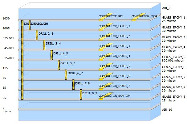
Automotive PCB SI and PI analysis
 Automotive PCB SI and PI analysis SI PI Analysis Signal Integrity S-Parameter Timing analysis Eye diagram Power Integrity Loop / Partial inductance DC IR-Drop AC PDN Impedance Power Aware SI Signal Integrity
Design Considerations for Highly Integrated 3D SiP for Mobile Applications
 Design Considerations for Highly Integrated 3D SiP for Mobile Applications FDIP, CA October 26, 2008 Joungho Kim at KAIST joungho@ee.kaist.ac.kr http://tera.kaist.ac.kr Contents I. Market and future direction
When Should You Apply 3D Planar EM Simulation?
 When Should You Apply 3D Planar EM Simulation? Agilent EEsof EDA IMS 2010 MicroApps Andy Howard Agilent Technologies 1 3D planar EM is now much more of a design tool Solves bigger problems and runs faster
Low Jitter, Low Emission Timing Solutions For High Speed Digital Systems. A Design Methodology
 Low Jitter, Low Emission Timing Solutions For High Speed Digital Systems A Design Methodology The Challenges of High Speed Digital Clock Design In high speed applications, the faster the signal moves through
The wireless industry
 From May 2007 High Frequency Electronics Copyright Summit Technical Media, LLC RF SiP Design Verification Flow with Quadruple LO Down Converter SiP By HeeSoo Lee and Dean Nicholson Agilent Technologies
Demystifying Vias in High-Speed PCB Design
 Demystifying Vias in High-Speed PCB Design Keysight HSD Seminar Mastering SI & PI Design db(s21) E H What is Via? Vertical Interconnect Access (VIA) An electrical connection between layers to pass a signal
High Speed Digital Design & Verification Seminar. Measurement fundamentals
 High Speed Digital Design & Verification Seminar Measurement fundamentals Agenda Sources of Jitter, how to measure and why Importance of Noise Select the right probes! Capture the eye diagram Why measure
EMC analysis workflow
 EMC analysis workflow Antonio Ciccomancini Scogna, CST of America antonio.ciccomancini@cst.com EMC/EMI Applications Emissions Susceptibility E3 Typical Emissions Issues 1 2 Image courtesy of Johnson Controls
Microcircuit Electrical Issues
 Microcircuit Electrical Issues Distortion The frequency at which transmitted power has dropped to 50 percent of the injected power is called the "3 db" point and is used to define the bandwidth of the
Strategies for High Density and High Speed Packaging. Ride the Wave Workshop
 Strategies for High Density and High Speed Packaging Ride the Wave Workshop Topics! Trends in Packaging! Common Design Challenges! Design through Software! Supply Plane Analysis with SIwave! Non-ideal
Signal Integrity Modeling and Simulation for IC/Package Co-Design
 Signal Integrity Modeling and Simulation for IC/Package Co-Design Ching-Chao Huang Optimal Corp. October 24, 2004 Why IC and package co-design? The same IC in different packages may not work Package is
DL-150 The Ten Habits of Highly Successful Designers. or Design for Speed: A Designer s Survival Guide to Signal Integrity
 Slide -1 Ten Habits of Highly Successful Board Designers or Design for Speed: A Designer s Survival Guide to Signal Integrity with Dr. Eric Bogatin, Signal Integrity Evangelist, Bogatin Enterprises, www.bethesignal.com
Power integrity is more than decoupling capacitors The Power Integrity Ecosystem. Keysight HSD Seminar Mastering SI & PI Design
 Power integrity is more than decoupling capacitors The Power Integrity Ecosystem Keysight HSD Seminar Mastering SI & PI Design Signal Integrity Power Integrity SI and PI Eco-System Keysight Technologies
EM Noise Mitigation in Electronic Circuit Boards and Enclosures
 EM Noise Mitigation in Electronic Circuit Boards and Enclosures Omar M. Ramahi, Lin Li, Xin Wu, Vijaya Chebolu, Vinay Subramanian, Telesphor Kamgaing, Tom Antonsen, Ed Ott, and Steve Anlage A. James Clark
The Ground Myth IEEE. Bruce Archambeault, Ph.D. IBM Distinguished Engineer, IEEE Fellow 18 November 2008
 The Ground Myth Bruce Archambeault, Ph.D. IBM Distinguished Engineer, IEEE Fellow barch@us.ibm.com 18 November 2008 IEEE Introduction Electromagnetics can be scary Universities LOVE messy math EM is not
DL-150 The Ten Habits of Highly Successful Designers. or Design for Speed: A Designer s Survival Guide to Signal Integrity
 Slide -1 Ten Habits of Highly Successful Board Designers or Design for Speed: A Designer s Survival Guide to Signal Integrity with Dr. Eric Bogatin, Signal Integrity Evangelist, Bogatin Enterprises, www.bethesignal.com
Practical Limitations of State of the Art Passive Printed Circuit Board Power Delivery Networks for High Performance Compute Systems
 Practical Limitations of State of the Art Passive Printed Circuit Board Power Delivery Networks for High Performance Compute Systems Presented by Chad Smutzer Mayo Clinic Special Purpose Processor Development
Innovations in EDA Webcast Series
 Welcome Innovations in EDA Webcast Series August 2, 2012 Jack Sifri MMIC Design Flow Specialist IC, Laminate, Package Multi-Technology PA Module Design Methodology Realizing the Multi-Technology Vision
Si-Interposer Collaboration in IC/PKG/SI. Eric Chen
 Si-Interposer Collaboration in IC/PKG/SI Eric Chen 4/Jul/2014 Design Overview U-bump Logic IC Mem IC C4 bump Logic IC Silicon/Organic substrate Interposer Mem IC CAP Package substrate Solder Ball VRM BGA
PI3DPX1207B Layout Guideline. Table of Contents. 1 Layout Design Guideline Power and GROUND High-speed Signal Routing...
 PI3DPX1207B Layout Guideline Table of Contents 1 Layout Design Guideline... 2 1.1 Power and GROUND... 2 1.2 High-speed Signal Routing... 3 2 PI3DPX1207B EVB layout... 8 3 Related Reference... 8 Page 1
Optimization of Wafer Level Test Hardware using Signal Integrity Simulation
 June 7-10, 2009 San Diego, CA Optimization of Wafer Level Test Hardware using Signal Integrity Simulation Jason Mroczkowski Ryan Satrom Agenda Industry Drivers Wafer Scale Test Interface Simulation Simulation
Design for EMI & ESD compliance DESIGN FOR EMI & ESD COMPLIANCE
 DESIGN FOR EMI & ESD COMPLIANCE All of we know the causes & impacts of EMI & ESD on our boards & also on our final product. In this article, we will discuss some useful design procedures that can be followed
EMC Simulation of Consumer Electronic Devices
 of Consumer Electronic Devices By Andreas Barchanski Describing a workflow for the EMC simulation of a wireless router, using techniques that can be applied to a wide range of consumer electronic devices.
EMI Reduction on an Automotive Microcontroller
 EMI Reduction on an Automotive Microcontroller Design Automation Conference, July 26 th -31 st, 2009 Patrice JOUBERT DORIOL 1, Yamarita VILLAVICENCIO 2, Cristiano FORZAN 1, Mario ROTIGNI 1, Giovanni GRAZIOSI
Electromagnetic Analysis of AC Coupling Capacitor Mounting Structures
 Simbeor Application Note #2008_02, April 2008 2008 Simberian Inc. Electromagnetic Analysis of AC Coupling Capacitor Mounting Structures Simberian, Inc. www.simberian.com Simbeor : Easy-to-Use, Efficient
Intro. to PDN Planning PCB Stackup Technology Series
 Introduction to Power Distribution Network (PDN) Planning Bill Hargin In-Circuit Design b.hargin@icd.com.au 425-301-4425 Intro. to PDN Planning 1. Intro/Overview 2. Bypass/Decoupling Strategy 3. Plane
EMI/EMC of Entire Automotive Vehicles and Critical PCB s. Makoto Suzuki Ansoft Corporation
 EMI/EMC of Entire Automotive Vehicles and Critical PCB s Makoto Suzuki Ansoft Corporation WT10_SI EMI/EMC of Entire Automotive Vehicles and Critical PCB s Akira Ohta, Toru Watanabe, Benson Wei Makoto Suzuki
Synthesis of Optimal On-Chip Baluns
 Synthesis of Optimal On-Chip Baluns Sharad Kapur, David E. Long and Robert C. Frye Integrand Software, Inc. Berkeley Heights, New Jersey Yu-Chia Chen, Ming-Hsiang Cho, Huai-Wen Chang, Jun-Hong Ou and Bigchoug
W2360EP/ET SIPro Signal Integrity EM Analysis W2359EP/ET PIPro Power Integrity EM Analysis
 Keysight Technologies Advanced Design System (ADS) W2360EP/ET SIPro Signal Integrity EM Analysis W2359EP/ET PIPro Power Integrity EM Analysis Data Sheet Composite EM technology delivers high-accuracy and
The Challenges of Differential Bus Design
 The Challenges of Differential Bus Design February 20, 2002 presented by: Arthur Fraser TechKnowledge Page 1 Introduction Background Historically, differential interconnects were often twisted wire pairs
High Speed Design Issues and Jitter Estimation Techniques. Jai Narayan Tripathi
 High Speed Design Issues and Jitter Estimation Techniques Jai Narayan Tripathi (jainarayan.tripathi@st.com) Outline Part 1 High-speed Design Issues Signal Integrity Power Integrity Jitter Power Delivery
JANUARY 28-31, 2013 SANTA CLARA CONVENTION CENTER. World s First LPDDR3 Enabling for Mobile Application Processors System
 JANUARY 28-31, 2013 SANTA CLARA CONVENTION CENTER World s First LPDDR3 Enabling for Mobile Application Processors System Contents Introduction Problem Statements at Early mobile platform Root-cause, Enablers
Modelling electromagnetic field coupling from an ESD gun to an IC
 Modelling electromagnetic field coupling from an ESD gun to an IC Ji Zhang #1, Daryl G Beetner #2, Richard Moseley *3, Scott Herrin *4 and David Pommerenke #5 # EMC Laboratory, Missouri University of Science
Chapter 12 Digital Circuit Radiation. Electromagnetic Compatibility Engineering. by Henry W. Ott
 Chapter 12 Digital Circuit Radiation Electromagnetic Compatibility Engineering by Henry W. Ott Forward Emission control should be treated as a design problem from the start, it should receive the necessary
EMC for Printed Circuit Boards
 9 Bracken View, Brocton Stafford, Staffs, UK tel: +44 (0)1785 660 247 fax +44 (0)1785 660 247 email: keith.armstrong@cherryclough.com web: www.cherryclough.com EMC for Printed Circuit Boards Basic and
Evaluation of Package Properties for RF BJTs
 Application Note Evaluation of Package Properties for RF BJTs Overview EDA simulation software streamlines the development of digital and analog circuits from definition of concept and estimation of required
Signal Integrity Design of TSV-Based 3D IC
 Signal Integrity Design of TSV-Based 3D IC October 24, 21 Joungho Kim at KAIST joungho@ee.kaist.ac.kr http://tera.kaist.ac.kr 1 Contents 1) Driving Forces of TSV based 3D IC 2) Signal Integrity Issues
A Novel Embedded Common-mode Filter for above GHz differential signals based on Metamaterial concept. Tzong-Lin Wu
 c //3 A Novel Embedded Common-mode Filter for above GHz differential signals based on Metamaterial concept Tzong-Lin Wu Professor Graduate Institute of Communication Engineering, National Taiwan University,
3 GHz Wide Frequency Model of Surface Mount Technology (SMT) Ferrite Bead for Power/Ground and I/O Line Noise Simulation of High-speed PCB
 Ferrite Bead for Power/Ground and I/O Line Noise Simulation of High-speed PCB") 3 GHz Wide Frequency Model of Surface Mount Technology (SMT) Ferrite Bead for Power/Ground and I/O Line Noise Simulation of High-speed PCB Tae Hong Kim, Hyungsoo Kim, Jun So Pak, and Joungho Kim Terahertz
3 GHz Wide Frequency Model of Surface Mount Technology (SMT) Ferrite Bead for Power/Ground and I/O Line Noise Simulation of High-speed PCB Tae Hong Kim, Hyungsoo Kim, Jun So Pak, and Joungho Kim Terahertz
10 COVER FEATURE CAD/EDA FOCUS
 10 COVER FEATURE CAD/EDA FOCUS Effective full 3D EMI analysis of complex PCBs by utilizing the latest advances in numerical methods combined with novel time-domain measurement technologies. By Chung-Huan
IC Decoupling and EMI Suppression using X2Y Technology
 IC Decoupling and EMI Suppression using X2Y Technology Summary Decoupling and EMI suppression of ICs is a complex system level engineering problem complicated by the desire for faster switching gates,
Presentation Abstract
 Presentation Abstract P1. IC to Victim Antenna Near-field Coupling Estimation - L. Li (S&T) In mixed radio-frequency (RF) and digital designs, noise from high-speed digital circuits can interfere with
Chip Package - PC Board Co-Design: Applying a Chip Power Model in System Power Integrity Analysis
 Chip Package - PC Board Co-Design: Applying a Chip Power Model in System Power Integrity Analysis Authors: Rick Brooks, Cisco, ricbrook@cisco.com Jane Lim, Cisco, honglim@cisco.com Udupi Harisharan, Cisco,
SSO Noise, Eye Margin, and Jitter Characterization for I/O Power Integrity
 DESIGNCON 2009 SSO Noise, Eye Margin, and Jitter Characterization for I/O Power Integrity Vishram S. Pandit, Intel Corporation [vishram.s.pandit@intel.com, (916)356-2059] Ashish N. Pardiwala, Intel Corporation
To learn statistical bit-error-rate (BER) simulation, BER link noise budgeting and using ADS to model high speed I/O link circuits
 simulation, BER link noise budgeting and using ADS to model high speed I/O link circuits") 1 ECEN 720 High-Speed Links: Circuits and Systems Lab6 Link Modeling with ADS Objective To learn statistical bit-error-rate (BER) simulation, BER link noise budgeting and using ADS to model high speed
1 ECEN 720 High-Speed Links: Circuits and Systems Lab6 Link Modeling with ADS Objective To learn statistical bit-error-rate (BER) simulation, BER link noise budgeting and using ADS to model high speed
Decoupling capacitor placement
 Decoupling capacitor placement Covered in this topic: Introduction Which locations need decoupling caps? IC decoupling Capacitor lumped model How to maximize the effectiveness of a decoupling cap Parallel
Applications of 3D Electromagnetic Modeling in Magnetic Recording: ESD and Signal Integrity
 Applications of 3D Electromagnetic Modeling in Magnetic Recording: ESD and Signal Integrity CST NORTH AMERICAN USERS FORUM John Contreras 1 and Al Wallash 2 Hitachi Global Storage Technologies 1. San Jose
Using Sonnet EM Analysis with Cadence Virtuoso in RFIC Design. Sonnet Application Note: SAN-201B July 2011
 Using Sonnet EM Analysis with Cadence Virtuoso in RFIC Design Sonnet Application Note: SAN-201B July 2011 Description of Sonnet Suites Professional Sonnet Suites Professional is an industry leading full-wave
CIRCUITS. Raj Nair Donald Bennett PRENTICE HALL
 POWER INTEGRITY ANALYSIS AND MANAGEMENT I CIRCUITS Raj Nair Donald Bennett PRENTICE HALL Upper Saddle River, NJ Boston Indianapolis San Francisco New York Toronto Montreal London Munich Paris Madrid Capetown
Top Ten EMC Problems
 Top Ten EMC Problems presented by: Kenneth Wyatt Sr. EMC Consultant EMC & RF Design, Troubleshooting, Consulting & Training 10 Northern Boulevard, Suite 1 Amherst, New Hampshire 03031 +1 603 578 1842 www.silent-solutions.com
DesignCon Control of Electromagnetic Radiation from Integrated Circuit Heat sinks. Cristian Tudor, Fidus Systems Inc.
 DesignCon 2009 Control of Electromagnetic Radiation from Integrated Circuit Heat sinks Cristian Tudor, Fidus Systems Inc. Cristian.Tudor@fidus.ca Syed. A. Bokhari, Fidus Systems Inc. Syed.Bokhari@fidus.ca
25Gb/s Ethernet Channel Design in Context:
 25Gb/s Ethernet Channel Design in Context: Channel Operating Margin (COM) Brandon Gore April 22 nd 2016 Backplane and Copper Cable Ethernet Interconnect Channel Compliance before IEEE 802.3bj What is COM?
AN ABSTRACT OF THE THESIS OF
 AN ABSTRACT OF THE THESIS OF Shannon Mark for the degree of Master of Science in Electrical and Computer Engineering presented on June 3, 2011. Title: Dual Referencing Guidelines to Minimize Power Delivery
Predicting and Controlling Common Mode Noise from High Speed Differential Signals
 Predicting and Controlling Common Mode Noise from High Speed Differential Signals Bruce Archambeault, Ph.D. IEEE Fellow, inarte Certified Master EMC Design Engineer, Missouri University of Science & Technology
W h i t e p a p e r. Authors. Engineer, E&SE - CoE, L&T Technology Services, Mysore. Engineer, E&SE - CoE, L&T Technology Services, Mysore
 W h i t e p a p e r Preface This paper describes a novel method of assessing the possible factors affecting the performance of High Speed Digital Circuit Boards in terms of maintaining the Signal Integrity
Design Fundamentals by A. Ciccomancini Scogna, PhD Suppression of Simultaneous Switching Noise in Power and Ground Plane Pairs
 Design Fundamentals by A. Ciccomancini Scogna, PhD Suppression of Simultaneous Switching Noise in Power and Ground Plane Pairs Photographer: Janpietruszka Agency: Dreamstime.com 36 Conformity JUNE 2007
The number of layers The number and types of planes (power and/or ground) The ordering or sequence of the layers The spacing between the layers
 The ordering or sequence of the layers The spacing between the layers") PCB Layer Stackup PCB layer stackup (the ordering of the layers and the layer spacing) is an important factor in determining the EMC performance of a product. The following four factors are important with
PCB Layer Stackup PCB layer stackup (the ordering of the layers and the layer spacing) is an important factor in determining the EMC performance of a product. The following four factors are important with
System Co-design and optimization for high performance and low power SoC s
 System Co-design and optimization for high performance and low power SoC s Siva S Kothamasu, Texas Instruments Inc, Dallas Snehamay Sinha, Texas Instruments Inc, Dallas Amit Brahme, Texas Instruments India
The Practical Limitations of S Parameter Measurements and the Impact on Time- Domain Simulations of High Speed Interconnects
 The Practical Limitations of S Parameter Measurements and the Impact on Time- Domain Simulations of High Speed Interconnects Dennis Poulin Anritsu Company Slide 1 Outline PSU Signal Integrity Symposium
Signal Integrity Tips and Techniques Using TDR, VNA and Modeling. Russ Kramer O.J. Danzy
 Signal Integrity Tips and Techniques Using TDR, VNA and Modeling Russ Kramer O.J. Danzy Simulation What is the Signal Integrity Challenge? Tx Rx Channel Asfiakhan Dreamstime.com - 3d People Communication
Multilayer VIA simulations using ADS Anurag Bhargava, Application Consultant, Agilent EEsof EDA, Agilent Technologies
 Multilayer VIA simulations using ADS Anurag Bhargava, Application Consultant, Agilent EEsof EDA, Agilent Technologies Many a time designers find themselves in pretty confusing start when it comes to simulating
Controlled Impedance Line Designer
 Heidi Barnes WW HSD Application Engineer Controlled Impedance Line Designer Stephen Slater HSD Product Manager EDA Simulation Tools for Power Integrity Agenda 1. Designing a channel for a desired impedance
Understanding the Unintended Antenna Behavior of a Product
 Understanding the Unintended Antenna Behavior of a Product Colin E. Brench Southwest Research Institute Electromagnetic Compatibility Research and Testing colin.brench@swri.org Radiating System Source
Plane Crazy, Part 2 BEYOND DESIGN. by Barry Olney
 by Barry Olney column BEYOND DESIGN Plane Crazy, Part 2 In my recent four-part series on stackup planning, I described the best configurations for various stackup requirements. But I did not have the opportunity
FPGA World Conference Stockholm 08 September John Steinar Johnsen -Josse- Senior Technical Advisor
 FPGA World Conference Stockholm 08 September 2015 John Steinar Johnsen -Josse- Senior Technical Advisor Agenda FPGA World Conference Stockholm 08 September 2015 - IPC 4101C Materials - Routing out from
How Long is Too Long? A Via Stub Electrical Performance Study
 How Long is Too Long? A Via Stub Electrical Performance Study Michael Rowlands, Endicott Interconnect Michael.rowlands@eitny.com, 607.755.5143 Jianzhuang Huang, Endicott Interconnect 1 Abstract As signal
Technical Report Printed Circuit Board Decoupling Capacitor Performance For Optimum EMC Design
 Technical Report Printed Circuit Board Decoupling Capacitor Performance For Optimum EMC Design Bruce Archambeault, Ph.D. Doug White Personal Systems Group Electromagnetic Compatibility Center of Competency
A Simulation Study of Simultaneous Switching Noise
 A Simulation Study of Simultaneous Switching Noise Chi-Te Chen 1, Jin Zhao 2, Qinglun Chen 1 1 Intel Corporation Network Communication Group, LOC4/19, 9750 Goethe Road, Sacramento, CA 95827 Tel: 916-854-1178,
Debugging EMI Using a Digital Oscilloscope. Dave Rishavy Product Manager - Oscilloscopes
 Debugging EMI Using a Digital Oscilloscope Dave Rishavy Product Manager - Oscilloscopes 06/2009 Nov 2010 Fundamentals Scope Seminar of DSOs Signal Fidelity 1 1 1 Debugging EMI Using a Digital Oscilloscope
Flip-Chip for MM-Wave and Broadband Packaging
 1 Flip-Chip for MM-Wave and Broadband Packaging Wolfgang Heinrich Ferdinand-Braun-Institut für Höchstfrequenztechnik (FBH) Berlin / Germany with contributions by F. J. Schmückle Motivation Growing markets
TABLE OF CONTENTS 1 Fundamentals Transmission Line Parameters... 29
 TABLE OF CONTENTS 1 Fundamentals... 1 1.1 Impedance of Linear, Time-Invariant, Lumped-Element Circuits... 1 1.2 Power Ratios... 2 1.3 Rules of Scaling... 5 1.3.1 Scaling of Physical Size... 6 1.3.1.1 Scaling
PARAMETER CONDITIONS TYPICAL PERFORMANCE Operating Supply Voltage 3.1V to 3.5V Supply Current V CC = 3.3V, LO applied 152mA
 DESCRIPTION LT5578 Demonstration circuit 1545A-x is a high linearity upconverting mixer featuring the LT5578. The LT 5578 is a high performance upconverting mixer IC optimized for output frequencies in
Signal Technologies 1
 Signal Technologies 1 Gunning Transceiver Logic (GTL) - evolution Evolved from BTL, the backplane transceiver logic, which in turn evolved from ECL (emitter-coupled logic) Setup of an open collector bus
Understanding, measuring, and reducing output noise in DC/DC switching regulators
 Understanding, measuring, and reducing output noise in DC/DC switching regulators Practical tips for output noise reduction Katelyn Wiggenhorn, Applications Engineer, Buck Switching Regulators Robert Blattner,
Characterization of Alternate Power Distribution Methods for 3D Integration
 Characterization of Alternate Power Distribution Methods for 3D Integration David C. Zhang, Madhavan Swaminathan, David Keezer and Satyanarayana Telikepalli School of Electrical and Computer Engineering,
Technology in Balance
 Technology in Balance A G1 G2 B Basic Structure Comparison Regular capacitors have two plates or electrodes surrounded by a dielectric material. There is capacitance between the two conductive plates within
Course Introduction. Content: 19 pages 3 questions. Learning Time: 30 minutes
 Course Introduction Purpose: This course discusses techniques that can be applied to reduce problems in embedded control systems caused by electromagnetic noise Objectives: Gain a basic knowledge about
Split Planes in Multilayer PCBs
 by Barry Olney coulmn BEYOND DESIGN Split Planes in Multilayer PCBs Creating split planes or isolated islands in the copper planes of multilayer PCBs at first seems like a good idea. Today s high-speed
Design Guide for High-Speed Controlled Impedance Circuit Boards
 IPC-2141A ASSOCIATION CONNECTING ELECTRONICS INDUSTRIES Design Guide for High-Speed Controlled Impedance Circuit Boards Developed by the IPC Controlled Impedance Task Group (D-21c) of the High Speed/High
ULTRASCALE DDR4 DE-EMPHASIS AND CTLE FEATURE OPTIMIZATION WITH STATISTICAL ENGINE FOR BER SPECIFICATION
 ULTRASCALE DDR4 DE-EMPHASIS AND CTLE FEATURE OPTIMIZATION WITH STATISTICAL ENGINE FOR BER SPECIFICATION Penglin Niu, penglin@xilinx.com Fangyi Rao, fangyi_rao@keysight.com Juan Wang, juanw@xilinx.com Gary