Electromagnetic Analysis and Verification of Probe Card Performance for First Pass System Success
|
|
|
- Jocelyn Grant
- 5 years ago
- Views:
Transcription


1 San Diego, CA Electromagnetic Analysis and Verification of Probe Card Performance for First Pass System Success Cristian Gozzi Application Engineer Manager
2 Introduction Today in Multi Probe wafer level, test is increasing with highly needed frequency capability demands: RF ICs Wafer sort (WLAN, Bluetooth, GPS, WiMax etc.) Final Test capabilities at EWS (multi Gigabit x second channel) Known Good Dice (KGD) New high speed ATE platform are already in the market This creates new and exciting ii challenges hll for Probe Card development IEEE SW Test Workshop 2
3 Objective Probe Card lead time becomes the main challenges for high frequency design: An example could be 5 6 working weeks for vertical PC This means a very short time window for Probe Card design (usually no more than 2 weeks) There is not enough time for prototyping and lab test/debug: Directly deliver good and full functional PC to customer The goal of this presentation is to show the usage of HF Simulation Methodology for addressing all design issues prior to manufacture Probe Card IEEE SW Test Workshop 3
4 Agenda Probe Card Design Flow for high speed performance Step by step Signal Integrity Analysis and simulation exampleson Probe Card system Step by step Power Integrity Analysis and simulation examples on Probe Card system High Frequency Probe Card example IEEE SW Test Workshop 4


5 Wafer DIE: Many HF Standard
6 Standard High Speed Data Rate Standard PCI Express 25/ / 8 USB Data Rate (GT/s) RapidIO 1.25 / 2.5 / / 5 / 6.25 DDR / 2133 HDMI 10.2 DisplayPort 1.62 / 2.7 / 5.4 InfiniBand 2.5 / 5 / 10 / / Serial ATA 1.5 / 3 / 6 Serial Attached SCSI 15/ / 6 Fibre Channel / / 4.25 / 8.5 / / GT/s Giga Transfer per Second raw bit rate (i.e. including balance bits due to 8B/10B encoding) IEEE SW Test Workshop 6


7 EWS System: Many Interconnections High speed test card Tx Coaxial cable Pogo Tower Clean, open, logical 1 & 0 at launch from transmitter + - Wafer DUT + - Rcv Load Board ATE SYSTEM + Needles Probe Head Probe Card PCB Logical 1 & 0 hard to t distinguish di ti i h att end interconnects; CLOSED EYE - PROBE CARD SYSTEM IEEE SW Test Workshop 7


8 Traditional PC Design Flow Layout Tool: Cadence, Mentor, Zuken, Altium PC manufacturing f t i EWS pass test? Drawbacks Money for PC re build Time for building them CUSTOMER CLAIMS Start again IEEE SW Test Workshop 8


9 High Frequency PC Design Flow Layout Tool: Cadence, Mentor, Zuken, Altium Virtual Prototype: Field Solver + Circuit Simulator Simulation: Fit Specs? Benefits No prototypes Save time and money Choose your strategy and e y itt by ssimulation u at o verify IEEE SW Test Workshop 9


10 HF PC Design Flow Requirements Design challenges to take into account during Probe Card development: Low voltage, high current Power Delivery System (PDS): Need to accurately control Power Integrity High frequency, high speed analog and digital signals: Need to accurately control Signal Integrity IEEE SW Test Workshop 10
11 Signal Integrity Check List Stackup analysis and Impedance control Frequency Domainanalysis analysis (Linear Network Analysis): Insertion Loss (IL), Return loss (RL), Coupling (X talk), Bandwidth performance ( 1dB; 3dB) Time Domain analysis (Transient analysis): TDR/TDT, rise/fall time, overshoot/undershoot, VIL/VOHmargin margin, ringing etc. Cross Talk analysis: Near End Xtalk (NEXT), Far End Xtalk (FEXT), noise from multiple aggressor SSNO analysis (Simultaneous Switching Noise Output ) EYE diagrams, BER, Jitter, Skew etc. IEEE SW Test Workshop 11
12 Power Integrity Check List Verify noise margin: IR Drop (DC) Power Plane impedance profile vs frequency (AC) Current distribution: High density current, bottleneck hot/heat source Decoupling capacitor solutions, tuning and optimization: Decoupling capacitor configuration, number of components, placement location, mounting effect, parasitic effect (ESR,ESL) Resonance modes: Identify location and frequency of natural cavity resonances thatexist between planes (power and ground bouncing) IEEE SW Test Workshop 12


 Solve the full Maxwell")
 Rigorous")


13 Which ElectroMagnetic Simulator? 3D Electromagnetic Field Solver E Need to accurately characterize and optimize p 3D interconnections ((needles, connectors, VIAs etc.) Solve the full Maxwell s Equations on each mesh element (FEM) Rigorous and accurate approach, but cannot be used for PDS characterization B t H J D t D B 0 2.5D Electromagnetic Field Solver Need to accurately characterize and optimize PCB power delivery system (impedance/inductance, decoupling capacitors etc.) Hybrid solver technologies is used for speed up simulation and characterize full PCB IEEE SW Test Workshop 13


14 ACTIVE LOAD CL AM P ACTIVE LOAD CL AM P ACTIVE LOAD CL AM P ACTIVE LOAD CL AM P ACTIVE LOAD CL AM P ACTIVE LOAD CL AM P ACTIVE LOAD CL AM P ACTIVE LOAD CL AM P ACTIVE LOAD CL AM P ACTIVE LOAD CL AM P V Circuit Environment: Simulate Entire EWS System POGO TESTER - ACTIVE LOADS LOAD PE POGO DQ5_PC LOAD PE POGO DQ0_PC EM Models S Parameters DUT - ACTIVE DRIVERS VCCQ_DUT VCCQ_DUT COMP DRIVER DRVIN DQ5_LOAD COMP DRIVER DRVIN DQ0_LOAD DQ0_DUT V192 DQ5_DUT V COMP COMP COMP DRIVER DRVIN DRIVER DRVIN DRIVER DRVIN LOAD PE DQ6_LOAD LOAD PE DQ7_LOAD LOAD PE DQ8_LOAD POGO POGO POGO DQ6_PC DQ7_PC DQ8_PC COMP COMP COMP DRIVER DRVIN DRIVER DRVIN DRIVER DRVIN LOAD LOAD LOAD PE DQ1_LOAD PE DQ2_LOAD PE DQ3_LOAD POGO POGO POGO DQ1_PC DQ2_PC DQ3_PC CH23_71_J47 DQ9_PC CH49_71_J47 DQ0_PC CH50_71_J47 DQ1_PC CH51_71_J47 DQ2_PC CH52_71_J47 DQ3_PC CH53_71_J47 DQ4_PC CH54_71_J47 DQ5_PC CH55_71_J47 DQ6_PC CH56_71_J47 DQ7_PC CH99_71_J47 DQ8_PC PPS1F_71_J47 VCCA_PC PPS2F_71_J47 VCCQ_PC Load Board CH23_71_GOMM24 CH49_71_GOMM24 CH50_71_GOMM24 CH51_71_GOMM24 CH52_71_GOMM24 CH53_71_GOMM24 CH54_71_GOMM24 CH55_71_GOMM24 CH56_71_GOMM24 CH99_71_GOMM24 GOMM24_PPS1F_71_Group GOMM24_PPS2F_71_Group R85 30mOhm L87 60nH V84 INTERPOSER CH23_71_GOMM24 CH23_71_INT-1 DQ9_DUT CH49_71_GOMM24 CH49_71_INT-1 DQ0_DUT CH50_71_GOMM24 CH50_71_INT-1 DQ1_DUT CH51_71_GOMM24 CH51_71_INT-1 DQ2_DUT CH52_71_GOMM24 CH52_71_INT-1 DQ3_DUT CH53_71_GOMM24 CH53_71_INT-1 DQ4_DUT CH54_71_GOMM24 CH54_71_INT-1 DQ5_DUT CH55_71_GOMM24 CH55_71_INT-1 DQ6_DUT CH56_71_GOMM24 CH56_71_INT-1 DQ7_DUT CH99_71_GOMM24 CH99_71_INT-1 GOMM24_PPS1F_71_Group DQ8_DUT INT-1_PPS1F_71_Group VCCA_DUT GOMM24_PPS2F_71_Group INT-1_PPS2F_71_Group VCCQ_DUT L88 R86 VCCQ_PC 4nH 4mOhm DQ1_DUT DQ2_DUT DQ3_DUT VCCQ_DUT VCCQ_DUT VCCQ_ DUT VCCQ_DUT 0 DQ6_DUT V DQ7_DUT V DQ8_DUT V200 0 VCCQ_DUT VCCQ_DUT VCCQ_ DUT VCCQ_DUT 0 V203 0 V204 0 V205 0 LOAD PE POGO DQ9_PC LOAD PE POGO DQ4_PC 0 DC=1.8V DQ4_DUT DQ9_DUT COMP DRIVER DRVIN DQ9_LOAD COMP DRIVER DRVIN DQ4_LOAD ATE model DUT models: IBIS or SPICE V V206 IEEE SW Test Workshop 14
15 Agenda Probe Card Design Flow for high speed performance Step by step Signal Integrity Analysis and simulation exampleson Probe Card system Step by step Power Integrity Analysis and simulation examples on Probe Card system High Frequency Probe Card example IEEE SW Test Workshop 15

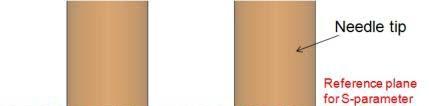


16 Signal Integrity: STEP #1 Needle Characterization bad good RETURN LOSS (Reflection Coefficient) IEEE SW Test Workshop 16

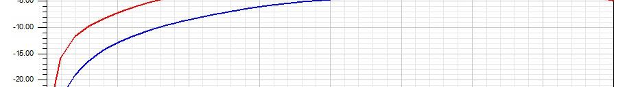


17 Signal Integrity: STEP #2 Needle Performance Optimization bd bad good Bandwidth improvment: from 200MHz to 1GHz Before After RETURN LOSS (Reflection Coefficient) 17


18 Signal Integrity: STEP #3 PCB Stackup Analysis and Controlled Impedance Differential Pair Target Zo=100Ohm IEEE SW Test Workshop 18


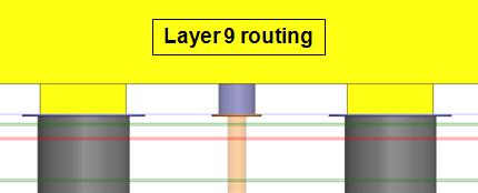
19 Signal Integrity: STEP #4 PCB Interconnection Optimization VIA stub impact: Routing Analysis Layer #5 vs Layer #9 IEEE SW Test Workshop 19


20 Signal Integrity: STEP #5 Cross Talk Analysis IEEE SW Test Workshop 20


21 Signal Integrity: STEP #6 TDR Analysis Impedance Improvement 21


22 Signal Integrity: STEP #6 EYE Analysis Gigabit Channel Improvement Eye source pattern PRBS15 with 8b10bEncoding, 80ps rise/fall time, 5 Gbps of Datarate, 2 Vpp and 100 Ohm differential load at Pogo pads IEEE SW Test Workshop 22
23 Agenda Probe Card Design Flow for high speed performance Step by step Signal Integrity Analysis and simulation exampleson Probe Card system Step by step Power Integrity Analysis and simulation examples on Probe Card system High Frequency Probe Card example IEEE SW Test Workshop 23


24 Power Integrity: STEP #1 Check DC PDS Specification What is the best DC PDS performance? Devices see voltage closet to nominal voltage Low IR drop Well balanced DC voltages among devices on the same rail Low Temperature Rise on Metal Low Current Density IEEE SW Test Workshop 24


25 DC Power Delivery System Simulation VDD Core Voltage Drop DC IR Analysis VDD Core Current Distribution High current density - bottleneck 30mV drop


26 Power Integrity: STEP #2 Check AC PDS Specification What is the best AC PDS performance? Low noise Low loop inductance Low and Flat impedance What are the PDS design issues? Number of Caps, location/placement l t Number of Vias, signals routing issue Component mounting effect PCB plane location/stack up Interposer effect V Noise PWR % ZTarget Current IEEE SW Test Workshop 26
27 Power Delivery System Topology IEEE SW Test Workshop 27
) SYZ Sw eep 1 Mag(Z(INT-1_PPS2F_71_Group,INT-1_PPS2F_71_Group)) SYZ Sw eep 1 m2 m3 Name")
![m1 X Y m1 263.0000 22.9463 m2 m3 339.0000 40.5410 410.0000 34.6249 10.00 Z Mag [Ohm] TARGET IMPEDANCE Compute Power Plane Self Impedance Z(f) 1.](/docs-images/89/100586887/images/28-2.jpg "00 VCCQ VCC 0.10 P k Impedance Peaks I d @ 250MHz, 250MH 340MH 340MHz and d 410MH 410MHz 0.01 1.00 10.00 100.00 Freq [MHz] IEEE SW Test Workshop 1000.")
28 AC Power Delivery System Simulation Impedance vs Frequency Analysis di VN L dt VN Z I SYZ Sweep 1 PWR Impedance Technoprobe INTERPOSER_PC_ Curve Info Mag(Z(INT-1_PPS1F_71_Group,INT-1_PPS1F_71_Group)) SYZ Sw eep 1 Mag(Z(INT-1_PPS2F_71_Group,INT-1_PPS2F_71_Group)) SYZ Sw eep 1 m2 m3 Name m1 X Y m m2 m Z Mag [Ohm] TARGET IMPEDANCE Compute Power Plane Self Impedance Z(f) 1.00 VCCQ VCC 0.10 P k Impedance Peaks I 250MHz, 250MH 340MH 340MHz and d 410MH 410MHz Freq [MHz] IEEE SW Test Workshop
29 AC Power Delivery System Simulation Resonance Modes Analysis PWR plane bouncing below DUT High Impedance hot spot area Decaps are mounted in this area: too far away from DUT VCCQ Resonant 250MHz IEEE SW Test Workshop 29
")

 [V] 1.80 1.60 1.")
 Delta(Y) Slope(Y) InvSlope(Y)")

30 AC Power Delivery System Simulation Wide DQ BUS causes SSN/SSO (power and ground bounce, AC drop) Simultaneous Switching Noise (SSN) Technoprobe POWER Switching Noise 2.40 m m2 t=4ns Curve Inf o V(VCCQ_DUT) Transient Allowed AC ripple noise V(VCCQ_DUT) [V] Name X Y m m Name Delta(X) Delta(Y) Slope(Y) InvSlope(Y) d(m1,m Time [ns] VCCQ VCC Fres=1/ t=250mhz 30


31 Power Integrity: STEP #3 Optimize Decoupling Capacitors Decoupling caps p p g capacitor? p Whyy optimize arrayy decoupling Chose the right number of decoupling capacitors to meet Ztarget Save space for signals routing, reduce design constrains and effort Chose the right package size, size value and mounting footprint Minimize mounting inductance, improve PWR impedance profile vs frequency IEEE SW Test Workshop 31


32 Decoupling Capacitor Selection Why use only classic 10nF, 100nF? Select the right capacitor values and package from Cap Vendor s library to obtain the best PWR Impedance profile vs Frequency MOUNTING DESIGN PACKAGE SIZE 32


33 Decaps Reduction Same Impedance Performance Reduced number off capacitors it IEEE SW Test Workshop 33
34 Agenda Probe Card Design Flow for high speed performance Step by step Signal Integrity Analysis and simulation exampleson Probe Card system Step by step Power Integrity Analysis and simulation examples on Probe Card system High Frequency Probe Card example IEEE SW Test Workshop 34


 802.")

35 HF Cantilever Probe Card for RF Wafer Sort Suitable forwireless RF front end wafer sort solution: Bluetooth (2.4 GHz) b/g/n (2.4GHz) y (3.7GHz) ac (<6GHz) WiMAX (2.3 GHz, GHz, GHz) Etc. IEEE SW Test Workshop 35
36 VNA Measurement FIRST PASS SYSTEM SUCCESS GOOD Performance up to 6GHz IEEE SW Test Workshop 36
37 SUMMARY Many high frequency standards are present in the market today, this require new methodology for Probe Card Design Usage of complete simulation environment allow Engineers to accurate check bothsignal and Power Integrity A step by step approach has been shown The speed up and accuracy of Electromagnetic Simulator, combined with Circuit Environment, allow to control ENTIRE EWS SYSTEM and Probe Card performance prior to manufacture FIRST PASS SYSTEM SUCCESS IEEE SW Test Workshop 37
38 Acknowledgment Thanks to Massimo Capodiferro (Ansoft Italy) for his support duringrecentrecent years on simulation setup/check Thanks to Flavio Maggioni (Technoprobe Italy) for his valuablecontribute on high frequency PCB design Future Works Continuous R&D simulation effort for improving high frequency PC performance and extend production of HF and KGD PC IEEE SW Test Workshop 38


39 Questions and Answers Q IEEE SW Test Workshop 39
Optimization of Wafer Level Test Hardware using Signal Integrity Simulation
 June 7-10, 2009 San Diego, CA Optimization of Wafer Level Test Hardware using Signal Integrity Simulation Jason Mroczkowski Ryan Satrom Agenda Industry Drivers Wafer Scale Test Interface Simulation Simulation
ANSYS CPS SOLUTION FOR SIGNAL AND POWER INTEGRITY
 ANSYS CPS SOLUTION FOR SIGNAL AND POWER INTEGRITY Rémy FERNANDES Lead Application Engineer ANSYS 1 2018 ANSYS, Inc. February 2, 2018 ANSYS ANSYS - Engineering simulation software leader Our industry reach
How to anticipate Signal Integrity Issues: Improve my Channel Simulation by using Electromagnetic based model
 How to anticipate Signal Integrity Issues: Improve my Channel Simulation by using Electromagnetic based model HSD Strategic Intent Provide the industry s premier HSD EDA software. Integration of premier
Relationship Between Signal Integrity and EMC
 Relationship Between Signal Integrity and EMC Presented by Hasnain Syed Solectron USA, Inc. RTP, North Carolina Email: HasnainSyed@solectron.com 06/05/2007 Hasnain Syed 1 What is Signal Integrity (SI)?
A Resonance-Free Power Delivery System Design Methodology applying 3D Optimized Extended Adaptive Voltage Positioning.
 A Resonance-Free Power Delivery System Design Methodology applying 3D Optimized Extended Adaptive Voltage Positioning Tao Xu Brad Brim Agenda Adaptive voltage positioning (AVP) Extended adaptive voltage
Probe Card Characterization in Time and Frequency Domain
 Gert Hohenwarter GateWave Northern, Inc. Probe Card Characterization in Time and Frequency Domain Company Logo 2007 San Diego, CA USA Objectives Illuminate differences between Time Domain (TD) and Frequency
Power integrity is more than decoupling capacitors The Power Integrity Ecosystem. Keysight HSD Seminar Mastering SI & PI Design
 Power integrity is more than decoupling capacitors The Power Integrity Ecosystem Keysight HSD Seminar Mastering SI & PI Design Signal Integrity Power Integrity SI and PI Eco-System Keysight Technologies
PCB Routing Guidelines for Signal Integrity and Power Integrity
 PCB Routing Guidelines for Signal Integrity and Power Integrity Presentation by Chris Heard Orange County chapter meeting November 18, 2015 1 Agenda Insertion Loss 101 PCB Design Guidelines For SI Simulation
Probing Techniques for Signal Performance Measurements in High Data Rate Testing
 Probing Techniques for Signal Performance Measurements in High Data Rate Testing K. Helmreich, A. Lechner Advantest Test Engineering Solutions GmbH Contents: 1 Introduction: High Data Rate Testing 2 Signal
Taking the Mystery out of Signal Integrity
 Slide - 1 Jan 2002 Taking the Mystery out of Signal Integrity Dr. Eric Bogatin, CTO, GigaTest Labs Signal Integrity Engineering and Training 134 S. Wolfe Rd Sunnyvale, CA 94086 408-524-2700 www.gigatest.com
Signal Integrity Design of TSV-Based 3D IC
 Signal Integrity Design of TSV-Based 3D IC October 24, 21 Joungho Kim at KAIST joungho@ee.kaist.ac.kr http://tera.kaist.ac.kr 1 Contents 1) Driving Forces of TSV based 3D IC 2) Signal Integrity Issues
Practical Limitations of State of the Art Passive Printed Circuit Board Power Delivery Networks for High Performance Compute Systems
 Practical Limitations of State of the Art Passive Printed Circuit Board Power Delivery Networks for High Performance Compute Systems Presented by Chad Smutzer Mayo Clinic Special Purpose Processor Development
Power Plane and Decoupling Optimization. Isaac Waldron
 Power Plane and Decoupling Optimization p Isaac Waldron Overview Frequency- and time-domain power distribution system specifications Decoupling design example Bare board Added d capacitors Buried Capacitance
Signal Integrity Modeling and Simulation for IC/Package Co-Design
 Signal Integrity Modeling and Simulation for IC/Package Co-Design Ching-Chao Huang Optimal Corp. October 24, 2004 Why IC and package co-design? The same IC in different packages may not work Package is
Automotive PCB SI and PI analysis
 Automotive PCB SI and PI analysis SI PI Analysis Signal Integrity S-Parameter Timing analysis Eye diagram Power Integrity Loop / Partial inductance DC IR-Drop AC PDN Impedance Power Aware SI Signal Integrity
Session 5 PCB Advancements And Opportunities
 Minimizing Socket & Board Inductance using a Novel decoupling Interposer 2007 Burn-in and Test Socket Workshop Nick Langston James Zhou, Hongjun Yao It is better to uncover a little than to cover a lot.
Validation Report Comparison of Eye Patterns Generated By Synopsys HSPICE and the Agilent PLTS
 Comparison of Eye Patterns Generated By Synopsys HSPICE and the Agilent PLTS Using: Final Inch Test/Eval Kit, Differential Pair - No Grounds Configuration, QTE-DP/QSE-DP, 5mm Stack Height (P/N FIK-QxE-04-01)
IEEE CX4 Quantitative Analysis of Return-Loss
 IEEE CX4 Quantitative Analysis of Return-Loss Aaron Buchwald & Howard Baumer Mar 003 Return Loss Issues for IEEE 0G-Base-CX4 Realizable Is the spec realizable with standard packages and I/O structures
DL-150 The Ten Habits of Highly Successful Designers. or Design for Speed: A Designer s Survival Guide to Signal Integrity
 Slide -1 Ten Habits of Highly Successful Board Designers or Design for Speed: A Designer s Survival Guide to Signal Integrity with Dr. Eric Bogatin, Signal Integrity Evangelist, Bogatin Enterprises, www.bethesignal.com
PDS Impact for DDR Low Cost Design
 PDS Impact for DDR3-1600 Low Cost Design Jack W.C. Lin Sr. AE Manager jackl@cadence.com Aug. g 13 2013 Cadence, OrCAD, Allegro, Sigrity and the Cadence logo are trademarks of Cadence Design Systems, Inc.
Optimizing Design of a Probe Card using a Field Solver
 Optimizing Design of a Probe Card using a Field Solver Rey Rincon, r-rincon@ti.com Texas Instruments 13020 Floyd Rd MS 3616 Dallas, TX. 75243 972-917-4303 Eric Bogatin, bogatin@ansoft.com Bill Beale, beale@ansoft.com
Reliable World Class Insights Your Silicon Valley Partner in Simulation ANSYS Sales, Consulting, Training & Support
 www.ozeninc.com info@ozeninc.com (408) 732 4665 1210 E Arques Ave St 207 Sunnyvale, CA 94085 Reliable World Class Insights Your Silicon Valley Partner in Simulation ANSYS Sales, Consulting, Training &
A Co-design Methodology of Signal Integrity and Power Integrity
 DesignCon 2006 A Co-design Methodology of Signal Integrity and Power Integrity Woong Hwan Ryu, Intel Corporation woong.hwan.ryu@intel.com Min Wang, Intel Corporation min.wang@intel.com 1 Abstract As PCB
High Speed Design Issues and Jitter Estimation Techniques. Jai Narayan Tripathi
 High Speed Design Issues and Jitter Estimation Techniques Jai Narayan Tripathi (jainarayan.tripathi@st.com) Outline Part 1 High-speed Design Issues Signal Integrity Power Integrity Jitter Power Delivery
Signal Integrity Tips and Techniques Using TDR, VNA and Modeling. Russ Kramer O.J. Danzy
 Signal Integrity Tips and Techniques Using TDR, VNA and Modeling Russ Kramer O.J. Danzy Simulation What is the Signal Integrity Challenge? Tx Rx Channel Asfiakhan Dreamstime.com - 3d People Communication
A Simulation Study of Simultaneous Switching Noise
 A Simulation Study of Simultaneous Switching Noise Chi-Te Chen 1, Jin Zhao 2, Qinglun Chen 1 1 Intel Corporation Network Communication Group, LOC4/19, 9750 Goethe Road, Sacramento, CA 95827 Tel: 916-854-1178,
Characterization of Alternate Power Distribution Methods for 3D Integration
 Characterization of Alternate Power Distribution Methods for 3D Integration David C. Zhang, Madhavan Swaminathan, David Keezer and Satyanarayana Telikepalli School of Electrical and Computer Engineering,
EMC cases study. Antonio Ciccomancini Scogna, CST of America CST COMPUTER SIMULATION TECHNOLOGY
 EMC cases study Antonio Ciccomancini Scogna, CST of America antonio.ciccomancini@cst.com Introduction Legal Compliance with EMC Standards without compliance products can not be released to the market Failure
Wideband On-die Power Supply Decoupling in High Performance DRAM
 Wideband On-die Power Supply Decoupling in High Performance DRAM Timothy M. Hollis, Senior Member of the Technical Staff Abstract: An on-die decoupling scheme, enabled by memory array cell technology,
The Challenges of Differential Bus Design
 The Challenges of Differential Bus Design February 20, 2002 presented by: Arthur Fraser TechKnowledge Page 1 Introduction Background Historically, differential interconnects were often twisted wire pairs
Thank you for downloading one of our ANSYS whitepapers we hope you enjoy it.
 Thank you! Thank you for downloading one of our ANSYS whitepapers we hope you enjoy it. Have questions? Need more information? Please don t hesitate to contact us! We have plenty more where this came from.
Measuring Hot TDR and Eye Diagrams with an Vector Network Analyzer?
 Measuring Hot TDR and Eye Diagrams with an Vector Network Analyzer? Gustaaf Sutorius Application Engineer Agilent Technologies gustaaf_sutorius@agilent.com Page 1 #TDR fit in Typical Digital Development
Understanding, measuring, and reducing output noise in DC/DC switching regulators
 Understanding, measuring, and reducing output noise in DC/DC switching regulators Practical tips for output noise reduction Katelyn Wiggenhorn, Applications Engineer, Buck Switching Regulators Robert Blattner,
DDR4 memory interface: Solving PCB design challenges
 DDR4 memory interface: Solving PCB design challenges Chang Fei Yee - July 23, 2014 Introduction DDR SDRAM technology has reached its 4th generation. The DDR4 SDRAM interface achieves a maximum data rate
High Speed Characterization Report
 High Speed Characterization Report MMCX-P-P-H-ST-TH1 mated with MMCX-J-P-H-ST-TH1 MMCX-P-P-H-ST-MT1 mated with MMCX-J-P-H-ST-MT1 MMCX-P-P-H-ST-SM1 mated with MMCX-J-P-H-ST-SM1 MMCX-P-P-H-ST-EM1 mated with
EMI. Chris Herrick. Applications Engineer
 Fundamentals of EMI Chris Herrick Ansoft Applications Engineer Three Basic Elements of EMC Conduction Coupling process EMI source Emission Space & Field Conductive Capacitive Inductive Radiative Low, Middle
Agilent Technologies High-Definition Multimedia
 Agilent Technologies High-Definition Multimedia Interface (HDMI) Cable Assembly Compliance Test Test Solution Overview Using the Agilent E5071C ENA Option TDR Last Update 013/08/1 (TH) Purpose This slide
EMI/EMC of Entire Automotive Vehicles and Critical PCB s. Makoto Suzuki Ansoft Corporation
 EMI/EMC of Entire Automotive Vehicles and Critical PCB s Makoto Suzuki Ansoft Corporation WT10_SI EMI/EMC of Entire Automotive Vehicles and Critical PCB s Akira Ohta, Toru Watanabe, Benson Wei Makoto Suzuki
Application Note. Signal Integrity Modeling. SCSI Connector and Cable Modeling from TDR Measurements
 Application Note SCSI Connector and Cable Modeling from TDR Measurements Signal Integrity Modeling SCSI Connector and Cable Modeling from TDR Measurements Dima Smolyansky TDA Systems, Inc. http://www.tdasystems.com
Closing the loop part 1: Why use simulation tools for high speed signal channel design?
 Closing the loop part 1: Why use simulation tools for high speed signal channel design? Riccardo Giacometti Application Engineer Agilent EEsof EDA Page 1 High Speed Digital Design Flow Pre-Layout w/channel
Intro. to PDN Planning PCB Stackup Technology Series
 Introduction to Power Distribution Network (PDN) Planning Bill Hargin In-Circuit Design b.hargin@icd.com.au 425-301-4425 Intro. to PDN Planning 1. Intro/Overview 2. Bypass/Decoupling Strategy 3. Plane
CIRCUITS. Raj Nair Donald Bennett PRENTICE HALL
 POWER INTEGRITY ANALYSIS AND MANAGEMENT I CIRCUITS Raj Nair Donald Bennett PRENTICE HALL Upper Saddle River, NJ Boston Indianapolis San Francisco New York Toronto Montreal London Munich Paris Madrid Capetown
Characterization Methodology for High Density Microwave Fixtures. Dr. Brock J. LaMeres, Montana State University
 DesignCon 2008 Characterization Methodology for High Density Microwave Fixtures Dr. Brock J. LaMeres, Montana State University lameres@ece.montana.edu Brent Holcombe, Probing Technology, Inc brent.holcombe@probingtechnology.com
JANUARY 28-31, 2013 SANTA CLARA CONVENTION CENTER. World s First LPDDR3 Enabling for Mobile Application Processors System
 JANUARY 28-31, 2013 SANTA CLARA CONVENTION CENTER World s First LPDDR3 Enabling for Mobile Application Processors System Contents Introduction Problem Statements at Early mobile platform Root-cause, Enablers
DesignCon Effect of Power Plane Inductance on Power Delivery Networks. Shirin Farrahi, Cadence Design Systems
 DesignCon 2019 Effect of Power Plane Inductance on Power Delivery Networks Shirin Farrahi, Cadence Design Systems shirinf@cadence.com, 978-262-6008 Ethan Koether, Oracle Corp ethan.koether@oracle.com Mehdi
ECE 546 Introduction
 ECE 546 Introduction Spring 2018 Jose E. Schutt-Aine Electrical & Computer Engineering University of Illinois jesa@illinois.edu ECE 546 Jose Schutt Aine 1 Future System Needs and Functions Auto Digital
The Practical Limitations of S Parameter Measurements and the Impact on Time- Domain Simulations of High Speed Interconnects
 The Practical Limitations of S Parameter Measurements and the Impact on Time- Domain Simulations of High Speed Interconnects Dennis Poulin Anritsu Company Slide 1 Outline PSU Signal Integrity Symposium
ULTRASCALE DDR4 DE-EMPHASIS AND CTLE FEATURE OPTIMIZATION WITH STATISTICAL ENGINE FOR BER SPECIFICATION
 ULTRASCALE DDR4 DE-EMPHASIS AND CTLE FEATURE OPTIMIZATION WITH STATISTICAL ENGINE FOR BER SPECIFICATION Penglin Niu, penglin@xilinx.com Fangyi Rao, fangyi_rao@keysight.com Juan Wang, juanw@xilinx.com Gary
3D IC-Package-Board Co-analysis using 3D EM Simulation for Mobile Applications
 3D IC-Package-Board Co-analysis using 3D EM Simulation for Mobile Applications Darryl Kostka, CST of America Taigon Song and Sung Kyu Lim, Georgia Institute of Technology Outline Introduction TSV Array
PDN Probes. P2100A/P2101A Data Sheet. 1-Port and 2-Port 50 ohm Passive Probes
 P2100A/P2101A Data Sheet PDN Probes 1-Port and 2-Port 50 ohm Passive Probes power integrity PDN impedance testing ripple PCB resonances transient step load stability and NISM noise TDT/TDR clock jitter
A Technical Discussion of TDR Techniques, S-parameters, RF Sockets, and Probing Techniques for High Speed Serial Data Designs
 A Technical Discussion of TDR Techniques, S-parameters, RF Sockets, and Probing Techniques for High Speed Serial Data Designs Presenter: Brian Shumaker DVT Solutions, LLC, 650-793-7083 b.shumaker@comcast.net
FIBRE CHANNEL CONSORTIUM
 FIBRE CHANNEL CONSORTIUM FC-PI-2 Clause 9 Electrical Physical Layer Test Suite Version 0.21 Technical Document Last Updated: August 15, 2006 Fibre Channel Consortium Durham, NH 03824 Phone: +1-603-862-0701
Power Distribution Network Design for Stratix IV GX and Arria II GX FPGAs
 Power Distribution Network Design for Stratix IV GX and Arria II GX FPGAs Transceiver Portfolio Workshops 2009 Question What is Your PDN Design Methodology? Easy Complex Historical Full SPICE simulation
USB 3.1 Cable-Connector Assembly Compliance Tests. Test Solution Overview Using the Keysight E5071C ENA Option TDR. Last Update 2015/02/06
 USB 3.1 Cable-Connector Assembly s Test Solution Overview Using the Keysight E5071C ENA Option TDR Last Update 015/0/06 Purpose This slide will show how to make measurements of USB 3.1 cable & connector
Ensuring Signal and Power Integrity for High-Speed Digital Systems
 Ensuring Signal and Power Integrity for High-Speed Digital Systems An EMC Perspective Christian Schuster Institut für Theoretische Elektrotechnik Technische Universität Hamburg-Harburg (TUHH) Invited Presentation
High Speed Digital Systems Require Advanced Probing Techniques for Logic Analyzer Debug
 JEDEX 2003 Memory Futures (Track 2) High Speed Digital Systems Require Advanced Probing Techniques for Logic Analyzer Debug Brock J. LaMeres Agilent Technologies Abstract Digital systems are turning out
Decoupling capacitor placement
 Decoupling capacitor placement Covered in this topic: Introduction Which locations need decoupling caps? IC decoupling Capacitor lumped model How to maximize the effectiveness of a decoupling cap Parallel
On Chip Active Decoupling Capacitors for Supply Noise Reduction for Power Gating and Dynamic Dual Vdd Circuits in Digital VLSI
 ELEN 689 606 Techniques for Layout Synthesis and Simulation in EDA Project Report On Chip Active Decoupling Capacitors for Supply Noise Reduction for Power Gating and Dynamic Dual Vdd Circuits in Digital
Signal Integrity Modeling and Measurement of TSV in 3D IC
 Signal Integrity Modeling and Measurement of TSV in 3D IC Joungho Kim KAIST joungho@ee.kaist.ac.kr 1 Contents 1) Introduction 2) 2.5D/3D Architectures with TSV and Interposer 3) Signal integrity, Channel
The Ground Myth IEEE. Bruce Archambeault, Ph.D. IBM Distinguished Engineer, IEEE Fellow 18 November 2008
 The Ground Myth Bruce Archambeault, Ph.D. IBM Distinguished Engineer, IEEE Fellow barch@us.ibm.com 18 November 2008 IEEE Introduction Electromagnetics can be scary Universities LOVE messy math EM is not
Effect of Power Noise on Multi-Gigabit Serial Links
 Effect of Power Noise on Multi-Gigabit Serial Links Ken Willis (kwillis@sigrity.com) Kumar Keshavan (ckumar@sigrity.com) Jack Lin (jackwclin@sigrity.com) Tariq Abou-Jeyab (tariqa@sigrity.com) Sigrity Inc.,
DL-150 The Ten Habits of Highly Successful Designers. or Design for Speed: A Designer s Survival Guide to Signal Integrity
 Slide -1 Ten Habits of Highly Successful Board Designers or Design for Speed: A Designer s Survival Guide to Signal Integrity with Dr. Eric Bogatin, Signal Integrity Evangelist, Bogatin Enterprises, www.bethesignal.com
High Speed Competitive Comparison Report. Samtec MMCX-J-P-H-ST-TH1 Mated With MMCX-P-P-H-ST-TH1 Competitor A (Mated Set) Competitor B (Mated Set)
 Competitor B (Mated Set)") High Speed Competitive Comparison Report Samtec MMCX-J-P-H-ST-TH1 Mated With MMCX-P-P-H-ST-TH1 Competitor A (Mated Set) Competitor B (Mated Set) REVISION DATE: January 6, 2005 TABLE OF CONTENTS Introduction...
High Speed Competitive Comparison Report Samtec MMCX-J-P-H-ST-TH1 Mated With MMCX-P-P-H-ST-TH1 Competitor A (Mated Set) Competitor B (Mated Set) REVISION DATE: January 6, 2005 TABLE OF CONTENTS Introduction...
Quick guide to Power. V1.2.1 July 29 th 2013
 Quick guide to Power Distribution ib ti Network Design V1.2.1 July 29 th 2013 High level High current, high transient Power Distribution Networks (PDN) need to be able to respond to changes and transients
The Technology Behind the World s Smallest 12V, 10A Voltage Regulator
 The Technology Behind the World s Smallest 12V, 10A Voltage Regulator A low profile voltage regulator achieving high power density and performance using a hybrid dc-dc converter topology Pradeep Shenoy,
Engineering the Power Delivery Network
 C HAPTER 1 Engineering the Power Delivery Network 1.1 What Is the Power Delivery Network (PDN) and Why Should I Care? The power delivery network consists of all the interconnects in the power supply path
Managing Complex Impedance, Isolation & Calibration for KGD RF Test Abstract
 Managing Complex Impedance, Isolation & Calibration for KGD RF Test Roger Hayward and Jeff Arasmith Cascade Microtech, Inc. Production Products Division 9100 SW Gemini Drive, Beaverton, OR 97008 503-601-1000,
UFS v2.0 PHY and Protocol Testing for Compliance. Copyright 2013 Chris Loberg, Tektronix
 UFS v2.0 PHY and Protocol Testing for Compliance Copyright 2013 Chris Loberg, Tektronix Agenda Introduction to MIPI Architecture & Linkage to UFS Compliance Testing Ecosystem UFS Testing Challenges Preparing
DesignCon Design of Gb/s Interconnect for High-bandwidth FPGAs. Sherri Azgomi, Altera Corporation
 DesignCon 2004 Design of 3.125 Gb/s Interconnect for High-bandwidth FPGAs Sherri Azgomi, Altera Corporation sazgomi@altera.com Lawrence Williams, Ph.D., Ansoft Corporation williams@ansoft.com CF-031505-1.0
Introduction to EMI/EMC Challenges and Their Solution
 Introduction to EMI/EMC Challenges and Their Solution Dr. Hany Fahmy HSD Application Expert Agilent Technologies Davy Pissort, K.U. Leuven Charles Jackson, Nvidia Charlie Shu, Nvidia Chen Wang, Nvidia
Constructing conducted emission models for integrated circuits
 Scholars' Mine Masters Theses Student Research & Creative Works Fall 2013 Constructing conducted emission models for integrated circuits Shuai Jin Follow this and additional works at: http://scholarsmine.mst.edu/masters_theses
Keysight MOI for USB Type-C Connectors & Cable Assemblies Compliance Tests (Type-C to Legacy Cable Assemblies)
") Revision 01.01 Jan-21, 2016 Universal Serial Bus Type-C TM Specification Revision 1.1 Keysight Method of Implementation (MOI) for USB Type-C TM Connectors and Cables Assemblies Compliance Tests Using Keysight
Revision 01.01 Jan-21, 2016 Universal Serial Bus Type-C TM Specification Revision 1.1 Keysight Method of Implementation (MOI) for USB Type-C TM Connectors and Cables Assemblies Compliance Tests Using Keysight
Basic Concepts C HAPTER 1
 C HAPTER 1 Basic Concepts Power delivery is a major challenge in present-day systems. This challenge is expected to increase in the next decade as systems become smaller and new materials are introduced
Low Jitter, Low Emission Timing Solutions For High Speed Digital Systems. A Design Methodology
 Low Jitter, Low Emission Timing Solutions For High Speed Digital Systems A Design Methodology The Challenges of High Speed Digital Clock Design In high speed applications, the faster the signal moves through
System Power Distribution Network Theory and Performance with Various Noise Current Stimuli Including Impacts on Chip Level Timing
 System Power Distribution Network Theory and Performance with Various Noise Current Stimuli Including Impacts on Chip Level Timing Larry Smith, Shishuang Sun, Peter Boyle, Bozidar Krsnik Altera Corp. Abstract-Power
Electrical Test Vehicle for High Density Fan-Out WLP for Mobile Application. Institute of Microelectronics 22 April 2014
 Electrical Test Vehicle for High Density Fan-Out WLP for Mobile Application Institute of Microelectronics 22 April 2014 Challenges for HD Fan-Out Electrical Design 15-20 mm 7 mm 6 mm SI/PI with multilayer
Demystifying Vias in High-Speed PCB Design
 Demystifying Vias in High-Speed PCB Design Keysight HSD Seminar Mastering SI & PI Design db(s21) E H What is Via? Vertical Interconnect Access (VIA) An electrical connection between layers to pass a signal
Case Study Package Design & SI/PI analysis
 Caliber Interconnect Solutions Design for perfection Case Study Package Design & SI/PI analysis Caliber Interconnect Solutions (Pvt) Ltd No 6,1 st Street Gandhi Nagar, Kavundampalayam, Coimbatore-30. Tamil
High Speed Characterization Report
 HLCD-20-XX-TD-BD-2 Mated with: LSHM-120-XX.X-X-DV-A Description: 0.50 mm Razor Beam High Speed Hermaphroditic Coax Cable Assembly Samtec, Inc. 2005 All Rights Reserved Table of Contents Cable Assembly
Keysight MOI for USB Type-C Connectors & Cable Assemblies Compliance Tests (Type-C to Legacy Cable Assemblies)
") Revision 01.00 Nov-24, 2015 Universal Serial Bus Type-C TM Specification Revision 1.1 Keysight Method of Implementation (MOI) for USB Type-C TM Connectors and Cables Assemblies Compliance Tests Using Keysight
Revision 01.00 Nov-24, 2015 Universal Serial Bus Type-C TM Specification Revision 1.1 Keysight Method of Implementation (MOI) for USB Type-C TM Connectors and Cables Assemblies Compliance Tests Using Keysight
Design of the Power Delivery System for Next Generation Gigahertz Packages
 Design of the Power Delivery System for Next Generation Gigahertz Packages Madhavan Swaminathan Professor School of Electrical and Computer Engg. Packaging Research Center madhavan.swaminathan@ece.gatech.edu
Schematic-Level Transmission Line Models for the Pyramid Probe
 Schematic-Level Transmission Line Models for the Pyramid Probe Abstract Cascade Microtech s Pyramid Probe enables customers to perform production-grade, on-die, full-speed test of RF circuits for Known-Good
Application Note 5525
 Using the Wafer Scale Packaged Detector in 2 to 6 GHz Applications Application Note 5525 Introduction The is a broadband directional coupler with integrated temperature compensated detector designed for
Narrowband Combline Filter Design with ANSYS HFSS
 Narrowband Combline Filter Design with ANSYS HFSS Daniel G. Swanson, Jr. DGS Associates, LLC Boulder, CO dan@dgsboulder.com www.dgsboulder.com Introduction N = 6 Inline, Cover Loaded, Combline Filter Single
Design and Optimization of a Novel 2.4 mm Coaxial Field Replaceable Connector Suitable for 25 Gbps System and Material Characterization up to 50 GHz
 Design and Optimization of a Novel 2.4 mm Coaxial Field Replaceable Connector Suitable for 25 Gbps System and Material Characterization up to 50 GHz Course Number: 13-WA4 David Dunham, Molex Inc. David.Dunham@molex.com
EMI Reduction on an Automotive Microcontroller
 EMI Reduction on an Automotive Microcontroller Design Automation Conference, July 26 th -31 st, 2009 Patrice JOUBERT DORIOL 1, Yamarita VILLAVICENCIO 2, Cristiano FORZAN 1, Mario ROTIGNI 1, Giovanni GRAZIOSI
An EM-aware methodology for a high-speed multi-protocol 28Gbps SerDes design with TSMC 16FFC
 An EM-aware methodology for a high-speed multi-protocol 28Gbps SerDes design with TSMC 16FFC Bud Hunter, SerDes Analog IC Design Manager, Wipro Kelly Damalou, Sr. Technical Account Manager, Helic TSMC
March 6-9, 2016 Hilton Phoenix / Mesa Hotel Mesa, Arizona Archive- Session 4
 Proceedings Archive March 6-9, 2016 Hilton Phoenix / Mesa Hotel Mesa, Arizona Archive- Session 4 2016 BiTS Workshop Image: Stiop / Dollarphotoclub Proceedings Archive Presentation / Copyright Notice The
HV739 ±100V 3.0A Ultrasound Pulser Demo Board
 HV79 ±00V.0A Ultrasound Pulser Demo Board HV79DB Introduction The HV79 is a monolithic single channel, high-speed, high voltage, ultrasound transmitter pulser. This integrated, high performance circuit
TITLE. Capturing (LP)DDR4 Interface PSIJ and RJ Performance. Image. Topic: Topic: John Ellis, Synopsys, Inc. Topic: malesuada blandit euismod.
DDR4 Interface PSIJ and RJ Performance. Image. Topic: Topic: John Ellis, Synopsys, Inc. Topic: malesuada blandit euismod.") TITLE Topic: o Nam elementum commodo mattis. Pellentesque Capturing (LP)DDR4 Interface PSIJ and RJ Performance malesuada blandit euismod. Topic: John Ellis, Synopsys, Inc. o o Nam elementum commodo mattis.
TITLE Topic: o Nam elementum commodo mattis. Pellentesque Capturing (LP)DDR4 Interface PSIJ and RJ Performance malesuada blandit euismod. Topic: John Ellis, Synopsys, Inc. o o Nam elementum commodo mattis.
Keysight Technologies Signal Integrity Tips and Techniques Using TDR, VNA and Modeling
 Keysight Technologies Signal Integrity Tips and Techniques Using, VNA and Modeling Article Reprint This article first appeared in the March 216 edition of Microwave Journal. Reprinted with kind permission
T est POST OFFICE BOX 1927 CUPERTINO, CA TEL E P H ONE (408) FAX (408) ARIES ELECTRONICS
 FAX (408) ARIES ELECTRONICS") G iga T est L abs POST OFFICE BOX 1927 CUPERTINO, CA 95015 TEL E P H ONE (408) 524-2700 FAX (408) 524-2777 ARIES ELECTRONICS BGA SOCKET (0.80MM TEST CENTER PROBE CONTACT) Final Report Electrical Characterization
G iga T est L abs POST OFFICE BOX 1927 CUPERTINO, CA 95015 TEL E P H ONE (408) 524-2700 FAX (408) 524-2777 ARIES ELECTRONICS BGA SOCKET (0.80MM TEST CENTER PROBE CONTACT) Final Report Electrical Characterization
F i n i s a r. Product Specification C.wire 120 Gb/s Parallel Active Optical Cable FCBGD10CD1Cxx
 Product Specification C.wire 120 Gb/s Parallel Active Optical Cable FCBGD10CD1Cxx PRODUCT FEATURES 12-channel full-duplex active optical cable Electrical interface only Multirate capability: 1.06Gb/s to
Strategies for High Density and High Speed Packaging. Ride the Wave Workshop
 Strategies for High Density and High Speed Packaging Ride the Wave Workshop Topics! Trends in Packaging! Common Design Challenges! Design through Software! Supply Plane Analysis with SIwave! Non-ideal
Decoupling Capacitance
 Decoupling Capacitance Nitin Bhardwaj ECE492 Department of Electrical and Computer Engineering Agenda Background On-Chip Algorithms for decap sizing and placement Based on noise estimation Decap modeling
LoopBack Relay. GLB363 Series. With Built-in AC Bypass Capacitors / DC LoopBack Relay
 GLB363 Series With Built-in AC Bypass Capacitors / DC SERIES DESIGNATION GLB363 RELAY TYPE, Sensitive Coil, Surface Mount Ground Shield and Stub pins with AC Bypass Capacitors or No capacitor DESCRIPTION
Advanced Product Design & Test for High-Speed Digital Devices
 Advanced Product Design & Test for High-Speed Digital Devices Presenters Part 1-30 min. Hidekazu Manabe Application Marketing Engineer Agilent Technologies Part 2-20 min. Mike Engbretson Chief Technology
TITLE. Image. Topic: Topic: Hee-Soo o LEE, Keysight Technologies Cindy Cui, Keysight Technologies
 TITLE Topic: Accurate o Nam elementum Statistical-Based commodo mattis. Pellentesque DDR4 Margin Estimation using malesuada SSN blandit Induced euismod. Jitter Model Topic: Hee-Soo o LEE, Keysight Technologies
IBIS in the Frequency Domain. Michael Mirmak Intel Corporation DAC IBIS Summit 2006 July 25, 2006
 IBIS in the Frequency Domain Michael Mirmak Intel Corporation DAC IBIS Summit 2006 July 25, 2006 Agenda Frequency Domain and Related Aspects Area 1: Maximum Switching Frequency Area 2: C_comp Stability
Modelling electromagnetic field coupling from an ESD gun to an IC
 Modelling electromagnetic field coupling from an ESD gun to an IC Ji Zhang #1, Daryl G Beetner #2, Richard Moseley *3, Scott Herrin *4 and David Pommerenke #5 # EMC Laboratory, Missouri University of Science