Design and Optimization of a Novel 2.4 mm Coaxial Field Replaceable Connector Suitable for 25 Gbps System and Material Characterization up to 50 GHz
|
|
|
- Emerald Lewis
- 6 years ago
- Views:
Transcription
1 Design and Optimization of a Novel 2.4 mm Coaxial Field Replaceable Connector Suitable for 25 Gbps System and Material Characterization up to 50 GHz Course Number: 13-WA4 David Dunham, Molex Inc. David.Dunham@molex.com +1-(630) Joon Lee, Molex Inc. Joon.Lee@molex.com +1-(317) Scott McMorrow, Teraspeed Consulting Group scott@teraspeed.com, +1- (401) Yuriy Shlepnev, Simberian Inc. shlepnev@simberian.com, +1-(702)
2 2.4mm Abstract With Data rates climbing to Gb/s and plans for 28 Gb/s, it becomes important to increase PCB fixtures from the typical 20 GHz to 50 GHz. There are several vendor Vector Network Analyzers that will sweep this high, but not many PCB launch connectors that can accurately launch these high frequencies. This paper will: Present modeling and validate data for a novel compression launch 2.4mm coaxial connector, functional up to 50GHz Introduce methods for analytical modeling and measurements for optimizing the PCB launch and escape, under the 2.4 mm connector. Demonstrate accurate broadband material characterization, using the method of generalized modal S-parameters, out to 50 GHz. The 2.4mm design includes a compression attach center conductor that does not require a solder attach to the PCB. The 2.4mm coax design meets all the standard 2.4mm mechanical interface standards, with a VSWR of 50 GHz back to back test method. This paper will review EDA analytically modeling methodology and results for the integrated 2.4mm coaxial connector with, several PCB layout designs. The final optimized PCB design was fabricated, measured and correlated to the analytical model. 2
3 Paper Overview This DesignCon paper will be presented in several parts Review of 2.4mm coaxial design and optimization modeling and results Two pcb optimization patterns have been modeled and measured. Optimization 1: Review of analytical models, results. Review of optimization 1 test board fab, test results and model to data correlation Optimization 1: Review of analytical models, results. Review of optimization 1 test board fab, test results and model to data correlation Practical material characterization and identification of dielectric loss and copper surface roughness 3

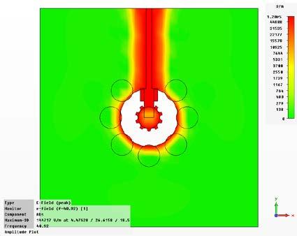
4 2.4mm Coaxial Design 4
5 2.4mm Coaxial Design 2.4MM CONNECTOR OVERVIEW Standard 2.4mm coaxial design using pressure contact attachment to the board. Uses two 0-80 UNF screws to mount the connector to the PCB with no solder requirement. Integrated center pin design which is capable to 1.2:1 VSWR at 50 GHz using back to back test method. 5


6 2.4mm Coaxial Design 6


7 2.4mm Coaxial Initial Design 7


8 2.4mm Coaxial Optimized Design 8
9 Optimization 1 Measure S-parameters of test fixture with 4 length of line segment. Optimization 1 has a simplified gnd pcb launch pattern 9

10 Optimization 1 Model review PCB Pattern 2.4mm PCB Launch Simplified Gnd Pattern 10 10

11 Optimization 1: Model Review PCB Stack 135mil Nelco EP Copper layers : 4 signals, 8 gnds Signal Layer 1 Signal Layer 2 Signal Layer 3 Signal Layer 4 Backdrill 11 11
12 Optimization 1: Modeled to Measured Results IL Plots Circuit1 Curve Info db(s(port1,port2)) LinearFrequency db(s(port3,port4)) LinearFrequency ANSOFT Signal Layer Y Red: Modeled Brown: Measured F [GHz] Signal Layer 4: Cavity Mode Resonance due to non optimized PCB via pattern 12

13 Optimization 1: TDR Results 13
14 Optimization 1 Observations Due to the high frequency bandwidth of this design it becomes very difficult to optimize both Frequency and Time domain capabilities. Optimization 1 tunes the TDR, leaving higher frequency resonances. 14

15 Optimization 2 Goals More aggressive optimization. Push cavity modes far above 50 GHz. Increase launch localization by providing better cavity ground containment. Optimize two connectors on trace to minimize halfwave end-to-end resonances. Provide complex internal compensation structures. 15


16 Areas of Optimization Top Layer Plane Layers Above/Below Trace Trace Layer 16

17 Return Loss Optimization Runs 17
18 TDR Results Across Sweeps 18

19 Optimization 2 Design Results Optimization results of two connectors separated by 300 mil of stripline trace to extend performance above 30 GHz. 19
20 Material parameters identification with GMSparameters Measure S-parameters of two test fixtures with different length of line segments S1 and S2 Transform S1 and S2 to the T-matrices T1 and T2, diagonalize the product of T1 and inversed T2 and compute GMS-parameters of the line difference Select material model and guess values of the model parameters Compute GMS-parameters of the line difference segment by solving Maxwell s equation for t-line cross-section (only propagation constants are needed) Adjust material parameters until computed GMS parameters fit measured GMS-parameters with the computed Simberian s patent pending 20 20
21 Measure S-parameters of two test fixtures with line segments (no calibration is required) S1 and T1 for line with length L1 L1 S1 T1 1 [S1/T1] 2 S2 and T2 for line with length L2 L2 S2 T2 1 [S2/T2] 2 T1 and T2 matrices are scattering T-parameters (computed directly from S-parameters) 21 21
22 Extract Generalized Modal T-parameters (GMT) and then GMS-Parameters Segment L1 T1 = TA TB 1 [T1] 2 1 [TA] [TB] 2 Segment L2 T 2 = TA GMT TB dl = L2 L1 1 [T2] 2 1 [TA] [GMT] [TB] 2 T 2 T1 = TA GMT TA ( 2 1 ) GMT = eigenvals T T Easy to compute! GMT is non-reflective modal T-matrix (normalized to the unknown characteristic impedances of the modes) For 1-conductor line we get: GMT T 0 11 = 1 0 T 11 GMSm = 11 T 11 0 Just 1 complex function! 0 T 1/10/ Simberian Inc. 22

23 Identifying dielectrics by fitting GMS-parameters Solve Maxwell s equations for 1-conductor line: dl GMSc ( Γ dl) 0 exp = exp( Γ dl) 0 Fit measured data: Only 1 complex function! GMSm 0 T = 11 T 11 0 Measured GMS-parameters of the segment can be directly fitted with the calculated GMS-parameters for material parameters identification Phase or group delay can be used to identify DK and insertion loss to identify LT or conductor roughness!
24 The GMS-parameters technique is the simplest possible Needs un-calibrated measurements for 2 t-lines with any geometry of cross-section and transitions No extraction of propagation constants (Gamma) from measured data (difficult, error-prone) No de-embedding of connectors and launches (difficult, error-prone) Needs the simplest numerical model Requires computation of only propagation constants No 3D electromagnetic models of the transitions Minimal number of smooth complex functions to match One parameter for single and two parameters for differential All reflection and modal transformation parameters are exactly zeros 24 24


25 What if launches or connectors in test fixtures are not identical? Numerical experiment to investigate the consequences of the non-identity Materials & Stackup Simple transition to 7-mil strip-line with pad (in L2) diameter changing from 8 to 22 mil with 3.5 mil discrete T0 8 mil T mil T2 15 mil T mil T4 22 mil 6 inch 8 inch Models of the launches different between 2 structures From simulated S-parameters of 2 structures with varying pad diameters we extract GMSparameters of 2-inch segment and compare it with the GMS-parameters of 2-inch segment computed directly 25 25

26 Effect of launch pad diameter on reflection from 8-inch test fixture In case of the t-line impedance close to 50-Ohm, the envelop of the reflection parameters is mostly defined by the reflection from the transition Pad diameter: T0 8 mil T mil T2 15 mil T mil T4 22 mil T4 T3 T4 T3 T0 T1 T2 T0 T1 T2 S11 of launches S11 of the 8-inch test fixtures Behavior of 6-inch fixture is similar 26 26
27 Effect of launch pad diameter on transmission through 8-inch test fixture Reflective launch lead to substantial difference in the insertion loss S12 of the test fixture S12 is not suitable for the material identification, even with relatively good launches! S12 of the 8-inch test fixtures Pad diameter: T0 8 mil T mil T2 15 mil T mil T4 22 mil T3 T0 T4 T1 T2 Phases are practically identical Group delays are substantially different due to reflections The result is similar for the 6-inch structure 27 27

28 GMS-parameters in case of identical launches Extracted GM transmission parameters of 2-inch segment are independent of the launch geometry as long as all 4 launches on 2 test fixtures are identical Launch with 8 mil pad Launch with 22 mil pad Stars 2-inch exact, circles computed from 2 test fixtures 28 28


29 What if launches on 6-inch fixture are different from launches on 8-inch fixture? Magnitude of Generalized Modal transmission and group delay look noisy Material identification may be possible only up to GHz Pad diameter: T0 8 mil; T mil GMS12 Group Delay Stars 2-inch segment Blue line launch T0 on 6- inch and T1 on 8-inch fixture 29 29

30 Another pair of launches (better) Generalized Modal transmission and group delay looks noisy Material identification may be possible only up to GHz Pad diameter: T mil;t2 15 mil GMS12 Group Delay Stars 2-inch segment Blue line launch T1 on 6- inch and T2 on 8-inch fixture 30 30


31 Worst pair of launches Generalized Modal transmission and group delay are extremely noisy Material identification may be possible only up to about 5-10 GHz Pad diameter: T mil; T4 22 mil GMS12 Group Delay Stars 2-inch segment Blue line launch T3 on 6- inch and T4 on 8-inch fixture 31 31
32 Example with acceptable difference in pad diameters Suitable for material identification up to 50 GHz Pad diameter: T2 15 mil; TM 13 mil GMS12 Group Delay Stars 2-inch segment Blue line launch T2 on 6-inch and TM on 8-inch fixture 32 32

33 Differences in S-parameters of launches and GMS-parameters extraction error Difference of reflections at launches 3.5 mil differences red lines T3-T2 T4-T3 T0-T1 T1-T2 TM-T2 2-mil difference: 13 and 15 mil The larger the difference in the launches, the larger the deviation of the extracted GMS-parameters from the GMS-parameters of 2-inch line 1/10/ Simberian Inc. 33
34 TDR of the test fixture can provide practical measure of non-identity for pre-qualification TDRs are computed with the rational macro-models and 20 ps ( ) Gaussian step 2 pairs have acceptable difference less than 1 Ohm Pad diameter: T0 8 mil T mil TM 13 mil T2 15 mil T mil T4 22 mil The difference in the launch impedances should be less than 1 Ohm for material identification up to 50 GHz 34 34

35 Material extraction structures at EP boards 2 board with the same stackup (4 signal & 8 GNDs), but different launches 6 test fixtures with 2, 4 and 6 inch strip line segments in Layer 1 and Layer 4 Signal Layer 1 Signal Layer 4 35
 and Gaussian step with 20 ps rise time 100% passive >99% reciprocal Resonances 6-inch fixture (green lines) has large variation in the impedance 2 and 4 inch structures")
36 Pre-qualification of launches on EP test board Launch 1, layer S1 TDR computed with rational macro-models (RMSE<0.005) and Gaussian step with 20 ps rise time 100% passive >99% reciprocal Resonances 6-inch fixture (green lines) has large variation in the impedance 2 and 4 inch structures are within 1 Ohm - suitable for the identification 36
 and Gaussian step with 20 ps rise time 100% passive >99% reciprocal Resonances 2-inch fixture (red lines) has large variation in the impedance 4 and 6 inch structures")
37 Pre-qualification of launches on EP test board Launch 1, layer S4 TDR computed with rational macro-models (RMSE<0.005) and Gaussian step with 20 ps rise time 100% passive >99% reciprocal Resonances 2-inch fixture (red lines) has large variation in the impedance 4 and 6 inch structures are within 1 Ohm - suitable for the identification 37
 and Gaussian step with 20 ps rise time 2-inch fixture (red lines) has large variation in the impedance 4 and 6 inch structures are within 1 Ohm - suitable for the")
38 Pre-qualification of launches on EP test board Launch 2, layer S1 100% passive >99% reciprocal No resonances TDR computed with rational macro-models (RMSE<0.005) and Gaussian step with 20 ps rise time 2-inch fixture (red lines) has large variation in the impedance 4 and 6 inch structures are within 1 Ohm - suitable for the identification 38
 and Gaussian step with 20 ps rise time 100% passive >99% reciprocal No resonances 6-inch fixture (green lines) is questionable (near launch) 2 and 4 inch structures")
39 Pre-qualification of launches on EP test board Launch 2, layer S4 TDR computed with rational macro-models (RMSE<0.005) and Gaussian step with 20 ps rise time 100% passive >99% reciprocal No resonances 6-inch fixture (green lines) is questionable (near launch) 2 and 4 inch structures are within 1 Ohm - suitable for the identification 39


40 GMS-parameters of 2-in line Extracted from different combinations of S-parameters measured for 2, 4 and 6 inch strip lines in layers S1 and S4 Bad launches & resonance blows off data above GHz 40

41 GMS-parameters of 4-in line Extracted from different combinations of S-parameters measured for 2 and 6 inch strip lines in layers S1 and S4 Bad launches & resonance blows off data above GHz 41

42 GMS-parameters from 3 best pairs Generalized Insertion Loss Generalized Group Delay 2-inch from 4 and 6 inch fixtures, launch 2, layers S1, S4 4-inch from 2 and 6 inch fixtures, launch 2, layer S4 4-inch from 2 and 6 inch fixtures, launch 2, layer S4 2-inch from 4 and 6 inch fixtures, launch 2, layers S1, S4 Already suitable for the identification, but can be further improved with post-processing 42

43 Fitted GMS-parameters from 3 best pairs Generalized Insertion Loss Generalized Group Delay 2-inch from 4 and 6 inch fixtures, launch 2, layers S1, S4 4-inch from 2 and 6 inch fixtures, launch 2, layer S4 4-inch from 2 and 6 inch fixtures, launch 2, layer S4 2-inch from 4 and 6 inch fixtures, launch 2, layers S1, S4 Now data are suitable for precise characterization of materials! 43
44 Practical Material Identification Step 1 Use group delay for preliminary Er Step 2 Evaluate potential variation Step 3 Identify low frequency characteristics Step 4 Adjust for dielectric loss Step 5 Final adjustment for conductor roughness 44
45 Practical Material Identification Step 1 Group Delay Preliminary Er Identification 45
46 Practical Material Identification Step 2 Evaluate variation 46
47 Practical Material Identification Step 3 Identify Low Frequency Characeristics 47
48 Practical Material Identification Step 4 Adjustment for Dielectric Loss 48
49 Practical Material Identification Step 5 Final Adjustment for Conductor Roughness 49
50 Conclusion A novel compression-launch 2.4mm coaxial connector, functional up to 50GHz, has been designed Methodology and design of optimal PCB launch and escape under the 2.4 mm connector are presented GMS-based material identification procedure is outlined and illustrated with practical examples Sensitivity of material identification to non-identities of the launches geometries is investigated theoretically and with practical examples Materials of a test board are identified from DC to 50 GHz 50
51 Authors David Dunham EE Director Molex Inc. Joon Lee Sr. RF Project Engineer Molex RF Division Scott McMorrow President Teraspeed Consulting Group LLC Yuriy Shlepnev President Simberian Inc 51
Guide to CMP-28/32 Simbeor Kit
 Guide to CMP-28/32 Simbeor Kit CMP-28 Rev. 4, Sept. 2014 Simbeor 2013.03, Aug. 10, 2014 Simbeor : Easy-to-Use, Efficient and Cost-Effective Electromagnetic Software Introduction Design of PCB and packaging
Yuriy Shlepnev, Simberian Inc Alfred Neves, Teraspeed Consulting Group
 DesignCon 2010 Practical identification of dispersive dielectric models with generalized modal S-parameters for analysis of interconnects in 6-100 Gb/s applications Yuriy Shlepnev, Simberian Inc. shlepnev@simberian.com,
Calibration and De-Embedding Techniques in the Frequency Domain
 Calibration and De-Embedding Techniques in the Frequency Domain Tom Dagostino tom@teraspeed.com Alfred P. Neves al@teraspeed.com Page 1 Teraspeed Labs Teraspeed Consulting Group LLC 2008 Teraspeed Consulting
A MATERIAL WORLD Modeling dielectrics and conductors for interconnects operating at Gbps
 TITLE A MATERIAL WORLD Modeling dielectrics and conductors for interconnects operating at 10-50 Gbps C. Nwachukwu, (Isola) Y. Shlepnev, (Simberian) S. McMorrow, (Teraspeed-Samtec) Image Practical PCB Material
Design Insights from Electromagnetic Analysis of Interconnects
 Design Insights from Electromagnetic Analysis of Interconnects Yuriy Shlepnev, Simberian Inc. shlepnev@simberian.com Front Range Signal Integrity Seminar, Longmont, CO October 3, 2013 10/8/2013 2013 Simberian
Lessons learned: How to Make Predictable PCB Interconnects for Data Rates of 50 Gbps and Beyond
 DesignCon 2014 Lessons learned: How to Make Predictable PCB Interconnects for Data Rates of 50 Gbps and Beyond Wendem Beyene, Rambus Inc. wbeyene@rambus.com Yeon-Chang Hahm, Rambus Inc. Jihong Ren, Rambus
The Design & Test of Broadband Launches up to 50 GHz on Thin & Thick Substrates
 The Performance Leader in Microwave Connectors The Design & Test of Broadband Launches up to 50 GHz on Thin & Thick Substrates Thin Substrate: 8 mil Rogers R04003 Substrate Thick Substrate: 30 mil Rogers
Controlled Impedance Line Designer
 Heidi Barnes WW HSD Application Engineer Controlled Impedance Line Designer Stephen Slater HSD Product Manager EDA Simulation Tools for Power Integrity Agenda 1. Designing a channel for a desired impedance
Challenges and Solutions for Removing Fixture Effects in Multi-port Measurements
 DesignCon 2008 Challenges and Solutions for Removing Fixture Effects in Multi-port Measurements Robert Schaefer, Agilent Technologies schaefer-public@agilent.com Abstract As data rates continue to rise
Optimization of Wafer Level Test Hardware using Signal Integrity Simulation
 June 7-10, 2009 San Diego, CA Optimization of Wafer Level Test Hardware using Signal Integrity Simulation Jason Mroczkowski Ryan Satrom Agenda Industry Drivers Wafer Scale Test Interface Simulation Simulation
A Signal Integrity Measuring Methodology in the Extraction of Wide Bandwidth Environmental Coefficients
 As originally published in the IPC APEX EXPO Conference Proceedings. A Signal Integrity Measuring Methodology in the Extraction of Wide Bandwidth Environmental Coefficients Eric Liao, Kuen-Fwu Fuh, Annie
Electromagnetic Analysis of AC Coupling Capacitor Mounting Structures
 Simbeor Application Note #2008_02, April 2008 2008 Simberian Inc. Electromagnetic Analysis of AC Coupling Capacitor Mounting Structures Simberian, Inc. www.simberian.com Simbeor : Easy-to-Use, Efficient
Validation Report Comparison of Eye Patterns Generated By Synopsys HSPICE and the Agilent PLTS
 Comparison of Eye Patterns Generated By Synopsys HSPICE and the Agilent PLTS Using: Final Inch Test/Eval Kit, Differential Pair - No Grounds Configuration, QTE-DP/QSE-DP, 5mm Stack Height (P/N FIK-QxE-04-01)
Characterization Methodology for High Density Microwave Fixtures. Dr. Brock J. LaMeres, Montana State University
 DesignCon 2008 Characterization Methodology for High Density Microwave Fixtures Dr. Brock J. LaMeres, Montana State University lameres@ece.montana.edu Brent Holcombe, Probing Technology, Inc brent.holcombe@probingtechnology.com
How to anticipate Signal Integrity Issues: Improve my Channel Simulation by using Electromagnetic based model
 How to anticipate Signal Integrity Issues: Improve my Channel Simulation by using Electromagnetic based model HSD Strategic Intent Provide the industry s premier HSD EDA software. Integration of premier
PCB Routing Guidelines for Signal Integrity and Power Integrity
 PCB Routing Guidelines for Signal Integrity and Power Integrity Presentation by Chris Heard Orange County chapter meeting November 18, 2015 1 Agenda Insertion Loss 101 PCB Design Guidelines For SI Simulation
Minimization of Reflection from AC Coupling Capacitors
 Simbeor Application Note #2008_04, September 2008 2008 Simberian Inc. Minimization of Reflection from AC Coupling Capacitors Simberian, Inc. www.simberian.com Simbeor : Easy-to-Use, Efficient and Cost-Effective
Effect of slots in reference planes on signal propagation in single and differential t-lines
 Simbeor Application Note #2007_09, November 2007 2007 Simberian Inc. Effect of slots in reference planes on signal propagation in single and differential t-lines Simberian, Inc. www.simberian.com Simbeor:
AN 766: Intel Stratix 10 Devices, High Speed Signal Interface Layout Design Guideline
 AN 766: Intel Stratix 10 Devices, High Speed Signal Interface Layout Subscribe Latest document on the web: PDF HTML Contents Contents Intel Stratix 10 Devices, High Speed Signal Interface Layout... 3 Intel
DesignCon East Feasibility of 40 to 50 Gbps NRZ Interconnect Design for Terabit Backplanes
 DesignCon East 2005 Feasibility of 40 to 50 Gbps NRZ Interconnect Design for Terabit Backplanes Roger Weiss, Paricon Technologies Corporation President, RWeiss@paricon-tech.com Scott McMorrow, Teraspeed
Design and experimental realization of the chirped microstrip line
 Chapter 4 Design and experimental realization of the chirped microstrip line 4.1. Introduction In chapter 2 it has been shown that by using a microstrip line, uniform insertion losses A 0 (ω) and linear
Signal Integrity
 www.tuc.com.tw Signal Integrity Factors influencing Signal Integrity 2 Studying Factors Studied the following factors Resin system Fabric Construction Conductor Moisture Temperature Test method 3 Resin
RF Characterization Report
 SMA-J-P-H-ST-MT1 Mated with: RF316-01SP1-01BJ1-0305 Description: 50-Ω SMA Board Mount Jack, Mixed Technology Samtec, Inc. 2005 All Rights Reserved Table of Contents Introduction...1 Product Description...1
CHAPTER 5 PRINTED FLARED DIPOLE ANTENNA
 CHAPTER 5 PRINTED FLARED DIPOLE ANTENNA 5.1 INTRODUCTION This chapter deals with the design of L-band printed dipole antenna (operating frequency of 1060 MHz). A study is carried out to obtain 40 % impedance
Aries Kapton CSP socket Cycling test
 Aries Kapton CSP socket Cycling test RF Measurement Results prepared by Gert Hohenwarter 10/21/04 1 Table of Contents TABLE OF CONTENTS... 2 OBJECTIVE... 3 METHODOLOGY... 3 Test procedures... 5 Setup...
Signal Integrity Tips and Techniques Using TDR, VNA and Modeling. Russ Kramer O.J. Danzy
 Signal Integrity Tips and Techniques Using TDR, VNA and Modeling Russ Kramer O.J. Danzy Simulation What is the Signal Integrity Challenge? Tx Rx Channel Asfiakhan Dreamstime.com - 3d People Communication
DesignCon Design of Gb/s Interconnect for High-bandwidth FPGAs. Sherri Azgomi, Altera Corporation
 DesignCon 2004 Design of 3.125 Gb/s Interconnect for High-bandwidth FPGAs Sherri Azgomi, Altera Corporation sazgomi@altera.com Lawrence Williams, Ph.D., Ansoft Corporation williams@ansoft.com CF-031505-1.0
Aries Kapton CSP socket
 Aries Kapton CSP socket Measurement and Model Results prepared by Gert Hohenwarter 5/19/04 1 Table of Contents Table of Contents... 2 OBJECTIVE... 3 METHODOLOGY... 3 Test procedures... 4 Setup... 4 MEASUREMENTS...
PCB Dielectric Material Selection and Fiber Weave Effect on High-Speed Channel Routing. Introduction
 PCB Dielectric Material Selection and Fiber Weave Effect on High-Speed Channel Routing May 2008, v1.0 Application Note 528 Introduction As data rates increase, designers are increasingly moving away from
Measuring PCB, Cable and Interconnect Impedance, Dielectric Constants, Velocity Factor, and Lengths
 Measuring PCB, Cable and Interconnect Impedance, Dielectric Constants, Velocity Factor, and Lengths Controlled impedance printed circuit boards (PCBs) often include a measurement coupon, which typically
High Speed Characterization Report
 ECDP-16-XX-L1-L2-2-2 Mated with: HSEC8-125-XX-XX-DV-X-XX Description: High-Speed 85Ω Differential Edge Card Cable Assembly, 30 AWG ACCELERATE TM Twinax Cable Samtec, Inc. 2005 All Rights Reserved Table
Practical Measurements of Dielectric Constant and Loss for PCB Materials at High Frequency
 8 th Annual Symposium on Signal Integrity PENN STATE, Harrisburg Center for Signal Integrity Practical Measurements of Dielectric Constant and Loss for PCB Materials at High Frequency Practical Measurements
High Speed Characterization Report
 HLCD-20-XX-TD-BD-2 Mated with: LSHM-120-XX.X-X-DV-A Description: 0.50 mm Razor Beam High Speed Hermaphroditic Coax Cable Assembly Samtec, Inc. 2005 All Rights Reserved Table of Contents Cable Assembly
Optimizing Design of a Probe Card using a Field Solver
 Optimizing Design of a Probe Card using a Field Solver Rey Rincon, r-rincon@ti.com Texas Instruments 13020 Floyd Rd MS 3616 Dallas, TX. 75243 972-917-4303 Eric Bogatin, bogatin@ansoft.com Bill Beale, beale@ansoft.com
High Speed Characterization Report
 ESCA-XX-XX-XX.XX-1-3 Mated with: SEAF8-XX-05.0-X-XX-2-K SEAM8-XX-S02.0-X-XX-2-K Description: 0.80 mm SEARAY High-Speed/High-Density Array Cable Assembly, 34 AWG Samtec, Inc. 2005 All Rights Reserved Table
Aries Center probe CSP socket Cycling test
 Aries Center probe CSP socket Cycling test RF Measurement Results prepared by Gert Hohenwarter 10/27/04 1 Table of Contents TABLE OF CONTENTS... 2 OBJECTIVE... 3 METHODOLOGY... 3 Test procedures... 5 Setup...
Aries CSP microstrip socket Cycling test
 Aries CSP microstrip socket Cycling test RF Measurement Results prepared by Gert Hohenwarter 2/18/05 1 Table of Contents TABLE OF CONTENTS... 2 OBJECTIVE... 3 METHODOLOGY... 3 Test procedures... 6 Setup...
VHDM & VHDM-L Series. High Speed. Electrical Characterization
 VHDM & VHDM-L Series High Speed Electrical Characterization HDM, VHDM & VHDM-HSD are trademarks or registered trademarks of Teradyne, Inc. Date: 2/14/2003 SCOPE 1. The scope of this document is to define
A Simplified QFN Package Characterization Technique
 Slide -1 A Simplified QFN Package Characterization Technique Dr. Eric Bogatin and Trevor Mitchell Bogatin Enterprises Dick Otte, President, Promex 8/1/10 Slide -2 Goal of this Project Develop a simple
PRELIMINARY PRELIMINARY
 Impedance Discontinuities of Right Angle Bends 90 degree, chamfered, and radial Augusto Panella Molex Incorporated Scott McMorrow SiQual, Inc. Introduction The results presented below are a portion of
DesignCon Differential PCB Structures using Measured TRL Calibration and Simulated Structure De-Embedding
 DesignCon 2007 Differential PCB Structures using Measured TRL Calibration and Simulated Structure De-Embedding Heidi Barnes, Verigy, Inc. heidi.barnes@verigy.com Dr. Antonio Ciccomancini, CST of America,
Electromagnetic Analysis of Decoupling Capacitor Mounting Structures with Simbeor
 Simbeor Application Note #2008_01, March 2008 2008 Simberian Inc. Electromagnetic Analysis of Decoupling Capacitor Mounting Structures with Simbeor Simberian, Inc. www.simberian.com Simbeor: Easy-to-Use,
High Speed Characterization Report
 ERCD_020_XX_TTR_TED_1_D Mated with: ERF8-020-05.0-S-DV-L Description: 0.8mm Edge Rate High Speed Coax Cable Assembly Samtec, Inc. 2005 All Rights Reserved Table of Contents Cable Assembly Overview... 1
The Basics of Patch Antennas, Updated
 The Basics of Patch Antennas, Updated By D. Orban and G.J.K. Moernaut, Orban Microwave Products www.orbanmicrowave.com Introduction This article introduces the basic concepts of patch antennas. We use
How Long is Too Long? A Via Stub Electrical Performance Study
 How Long is Too Long? A Via Stub Electrical Performance Study Michael Rowlands, Endicott Interconnect Michael.rowlands@eitny.com, 607.755.5143 Jianzhuang Huang, Endicott Interconnect 1 Abstract As signal
High Speed Characterization Report
 PCRF-064-XXXX-EC-SMA-P-1 Mated with: PCIE-XXX-02-X-D-TH Description: PCI Express Cable Assembly, Low Loss Microwave Cable Samtec, Inc. 2005 All Rights Reserved Table of Contents Cable Assembly Overview...
Aries QFP microstrip socket
 Aries QFP microstrip socket Measurement and Model Results prepared by Gert Hohenwarter 2/18/05 1 Table of Contents Table of Contents... 2 OBJECTIVE... 3 METHODOLOGY... 3 Test procedures... 4 Setup... 4
Impedance-Controlled Routing. Contents
 Impedance-Controlled Routing Contents Do I Need Impedance Controlled Routing? How do I Control the Impedances? Impedance Matching the Components What Determines the Routing Impedance? Calculating the Routing
25Gb/s Ethernet Channel Design in Context:
 25Gb/s Ethernet Channel Design in Context: Channel Operating Margin (COM) Brandon Gore April 22 nd 2016 Backplane and Copper Cable Ethernet Interconnect Channel Compliance before IEEE 802.3bj What is COM?
Application Note 5525
 Using the Wafer Scale Packaged Detector in 2 to 6 GHz Applications Application Note 5525 Introduction The is a broadband directional coupler with integrated temperature compensated detector designed for
A Technical Discussion of TDR Techniques, S-parameters, RF Sockets, and Probing Techniques for High Speed Serial Data Designs
 A Technical Discussion of TDR Techniques, S-parameters, RF Sockets, and Probing Techniques for High Speed Serial Data Designs Presenter: Brian Shumaker DVT Solutions, LLC, 650-793-7083 b.shumaker@comcast.net
3M Shielded Controlled Impedance (SCI) Latch/Eject Header 2 mm Development Kit Instructions
 Latch/Eject Header 2 mm Development Kit Instructions") 3M Shielded Controlled Impedance (SCI) Latch/Eject Header 2 mm Development Kit Instructions Contents 1.0 Purpose....................................... 1 2.0 Development Kits..................................
3M Shielded Controlled Impedance (SCI) Latch/Eject Header 2 mm Development Kit Instructions Contents 1.0 Purpose....................................... 1 2.0 Development Kits..................................
EE290C - Spring 2004 Advanced Topics in Circuit Design
 EE290C - Spring 2004 Advanced Topics in Circuit Design Lecture #3 Measurements with VNA and TDR Ben Chia Tu-Th 4 5:30pm 531 Cory Agenda Relationships between time domain and frequency domain TDR Time Domain
High Speed Characterization Report
 QTH-030-01-L-D-A Mates with QSH-030-01-L-D-A Description: High Speed Ground Plane Header Board-to-Board, 0.5mm (.0197 ) Pitch, 5mm (.1969 ) Stack Height Samtec, Inc. 2005 All Rights Reserved Table of Contents
High Speed Characterization Report
 SSW-1XX-22-X-D-VS Mates with TSM-1XX-1-X-DV-X Description: Surface Mount Terminal Strip,.1 [2.54mm] Pitch, 13.59mm (.535 ) Stack Height Samtec, Inc. 25 All Rights Reserved Table of Contents Connector Overview...
Demystifying Vias in High-Speed PCB Design
 Demystifying Vias in High-Speed PCB Design Keysight HSD Seminar Mastering SI & PI Design db(s21) E H What is Via? Vertical Interconnect Access (VIA) An electrical connection between layers to pass a signal
Design and Demonstration of a Passive, Broadband Equalizer for an SLED Chris Brinton, Matthew Wharton, and Allen Katz
 Introduction Design and Demonstration of a Passive, Broadband Equalizer for an SLED Chris Brinton, Matthew Wharton, and Allen Katz Wavelength Division Multiplexing Passive Optical Networks (WDM PONs) have
New Configurations for RF/Microwave Filters
 New Configurations for RF/Microwave Filters Presented by: Jeremy Fejfar Applications Engineer CST of America, Inc. 1 www.cst.com Sep-06 Outline Introduction Conventional Filter Theory Need for Folded Transmission
Detailed Design Review
 Detailed Design Review P09343 Microwave Data II Joel Barry Amanda Kristoff Mia Mujezinovic Michael Pecoraro 1 P09343 Microwave Data II Technical Review Agenda Meeting Purpose: This meeting is to review
1000BASE-T1 EMC Test Specification for Common Mode Chokes
 IEEE 1000BASE-T1 EMC Test Specification for Common Mode Chokes Version 1.0 Author & Company Dr. Bernd Körber, FTZ Zwickau Title 1000BASE-T1 EMC Test Specification for Common Mode Chokes Version 1.0 Date
Characterizing Non-Standard Impedance Channels with 50 Ohm Instruments
 Characterizing Non-Standard Impedance Channels with 50 Ohm Instruments Julian Ferry, Jim Nadolny, Craig Rapp: Samtec Inc. Mike Resso, O.J. Danzy: Agilent Technologies Introduction Emerging systems are
SMA Self-Fixture End Launch Connectors
 SMA Self-Fixture End Launch Connectors INTRODUCTION / APPLICATIONS Applications for these connectors include: An ideal solution for design engineers who are obligated to cut manufacturing costs and complexity
High Speed Characterization Report
 PCIEC-XXX-XXXX-EC-EM-P Mated with: PCIE-XXX-02-X-D-TH Description: 1.00 mm PCI Express Internal Cable Assembly, 30 AWG Twinax Ribbon Cable Samtec, Inc. 2005 All Rights Reserved Table of Contents Cable
Custom Interconnects Fuzz Button with Hardhat Test Socket/Interposer 1.00 mm pitch
 Custom Interconnects Fuzz Button with Hardhat Test Socket/Interposer 1.00 mm pitch Measurement and Model Results prepared by Gert Hohenwarter 12/14/2015 1 Table of Contents TABLE OF CONTENTS...2 OBJECTIVE...
QUADSPLITTER AND IN-LINE QUADSPLITTER
 QUADSPLITTER AND IN-LINE QUADSPLITTER technical characteristics specifications temperature rating: -55 c to + 5 c corrosion: MIL-STD-0 Method 0, Test Condition B shock: MIL-STD-0 Method, Test Condition
PI3HDMIxxx 4-Layer PCB Layout Guideline for HDMI Products
 PI3HDMIxxx 4-Layer PCB Layout Guideline for HDMI Products Introduction The differential trace impedance of HDMI is specified at 100Ω±15% in Test ID 8-8 in HDMI Compliance Test Specification Rev.1.2a and
Practical Design Considerations for Dense, High-Speed, Differential Stripline PCB Routing Related to Bends, Meanders and Jog-outs
 Practical Design Considerations for Dense, High-Speed, Differential Stripline PCB Routing Related to Bends, Meanders and Jog-outs AUTHORS Michael J. Degerstrom, Mayo Clinic degerstrom.michael@mayo.edu
DL-150 The Ten Habits of Highly Successful Designers. or Design for Speed: A Designer s Survival Guide to Signal Integrity
 Slide -1 Ten Habits of Highly Successful Board Designers or Design for Speed: A Designer s Survival Guide to Signal Integrity with Dr. Eric Bogatin, Signal Integrity Evangelist, Bogatin Enterprises, www.bethesignal.com
Validation & Analysis of Complex Serial Bus Link Models
 Validation & Analysis of Complex Serial Bus Link Models Version 1.0 John Pickerd, Tektronix, Inc John.J.Pickerd@Tek.com 503-627-5122 Kan Tan, Tektronix, Inc Kan.Tan@Tektronix.com 503-627-2049 Abstract
Microwave Metrology -ECE 684 Spring Lab Exercise T: TRL Calibration and Probe-Based Measurement
 ab Exercise T: TR Calibration and Probe-Based Measurement In this project, you will measure the full phase and magnitude S parameters of several surface mounted components. You will then develop circuit
OMNETICS CONNECTOR CORPORATION PART I - INTRODUCTION
 OMNETICS CONNECTOR CORPORATION HIGH-SPEED CONNECTOR DESIGN PART I - INTRODUCTION High-speed digital connectors have the same requirements as any other rugged connector: For example, they must meet specifications
High Speed Competitive Comparison Report. Samtec MMCX-J-P-H-ST-TH1 Mated With MMCX-P-P-H-ST-TH1 Competitor A (Mated Set) Competitor B (Mated Set)
 Competitor B (Mated Set)") High Speed Competitive Comparison Report Samtec MMCX-J-P-H-ST-TH1 Mated With MMCX-P-P-H-ST-TH1 Competitor A (Mated Set) Competitor B (Mated Set) REVISION DATE: January 6, 2005 TABLE OF CONTENTS Introduction...
High Speed Competitive Comparison Report Samtec MMCX-J-P-H-ST-TH1 Mated With MMCX-P-P-H-ST-TH1 Competitor A (Mated Set) Competitor B (Mated Set) REVISION DATE: January 6, 2005 TABLE OF CONTENTS Introduction...
surface mount chip capacitor model
 surface mount chip capacitor model Model Features* Broadband validation: DC 30 GHz Equivalent circuit based Applicable for horizontal mounted capacitors Substrate scalable: (1 H/Er 16.7 mil) Part value
SURFACE MOUNT HIGH REPEATABILITY, BROADBAND TO-5 RELAYS DPDT
 SURFACE MOUNT HIGH REPEATABILITY, BROADBAND TO-5 RELAYS DPDT SERIES GRF300 GRF300D GRF300DD GRF303 GRF303D GRF303DD RELAY TYPE Repeatable, RF relay Repeatable, RF relay with internal diode for coil transient
L-BAND COPLANAR SLOT LOOP ANTENNA FOR INET APPLICATIONS
 L-BAND COPLANAR SLOT LOOP ANTENNA FOR INET APPLICATIONS Jeyasingh Nithianandam Electrical and Computer Engineering Department Morgan State University, 500 Perring Parkway, Baltimore, Maryland 5 ABSTRACT
ECE 145A/218A, Lab Project #1a: passive Component Test.
 ECE 145A/218A, Lab Project #1a: passive Component Test. September 28, 2017 OVERVIEW... 2 GOALS:... 2 PRECAUTIONS TO AVOID INSTRUMENT DAMAGE... 2 SAFETY PRECAUTIONS... 2 READING:... 3 NETWORK ANALYZER CALIBRATION...
Keysight Technologies Signal Integrity Tips and Techniques Using TDR, VNA and Modeling
 Keysight Technologies Signal Integrity Tips and Techniques Using, VNA and Modeling Article Reprint This article first appeared in the March 216 edition of Microwave Journal. Reprinted with kind permission
High Data Rate Characterization Report
 High Data Rate Characterization Report ERDP-013-39.37-TTR-STL-1-D Mated with: ERF8-013-05.0-S-DV-DL-L and ERM8-013-05.0-S-DV-DS-L Description: Edge Rate Twin-Ax Cable Assembly, 0.8mm Pitch Samtec, Inc.
Application Note 5499
 MGA-31389 and MGA-31489 High-Gain Driver Amplifier Using Avago MGA-31389 and MGA-31489 Application Note 5499 Introduction The MGA-31389 and MGA-31489 from Avago Technologies are.1 Watt flat-gain driver
Design of optimal differential viaholes for 6-plane board
 Simbeor Application Note #2007_08, October 2007 2007 Simberian Inc. Design of optimal differential viaholes for 6-plane board Simberian, Inc. www.simberian.com Simbeor: Easy-to-Use, Efficient and Cost-Effective
Introduction to RF Measurement and Nonideal Components The Vector Network Analyzer UCSB - ECE145A/ECE218A Winter 2007
 Goals: Introduction to RF Measurement and Nonideal Components The Vector Network Analyzer UCSB - ECE145A/ECE218A Winter 2007 (a) Introduction to the vector network analyzer and measurement of S-parameters.
There is a twenty db improvement in the reflection measurements when the port match errors are removed.
 ABSTRACT Many improvements have occurred in microwave error correction techniques the past few years. The various error sources which degrade calibration accuracy is better understood. Standards have been
CHAPTER 4. Practical Design
 CHAPTER 4 Practical Design The results in Chapter 3 indicate that the 2-D CCS TL can be used to synthesize a wider range of characteristic impedance, flatten propagation characteristics, and place passive
ECE 4265/6265 Laboratory Project 7 Network Analyzer Calibration
 ECE 4265/6265 Laboratory Project 7 Network Analyzer Calibration Objectives The purpose of this lab is to introduce the concepts of calibration and error correction for microwave s-parameter measurements.
Making Sense of Laminate Dielectric Properties By Michael J. Gay and Richard Pangier Isola
 Making Sense of Laminate Dielectric Properties By Michael J. Gay and Richard Pangier Isola Abstract System operating speeds continue to increase as a function of the consumer demand for such technologies
High-Power Directional Couplers with Excellent Performance That You Can Build
 High-Power Directional Couplers with Excellent Performance That You Can Build Paul Wade W1GHZ 2010 w1ghz@arrl.net A directional coupler is used to sample the RF energy travelling in a transmission line
Considerations in High-Speed High Performance Die-Package-Board Co-Design. Jenny Jiang Altera Packaging Department October 2014
 Considerations in High-Speed High Performance Die-Package-Board Co-Design Jenny Jiang Altera Packaging Department October 2014 Why Co-Design? Complex Multi-Layer BGA Package Horizontal and vertical design
surface mount chip capacitor model
 S (db) CAP-PPI-78N- surface mount chip capacitor model Model Features* Broadband validation: DC 4 GHz Equivalent circuit based Substrate scalable:(.9 H/Er 6.5 mil) Part value scalable: (. to pf) Land Pattern
Design Guide for High-Speed Controlled Impedance Circuit Boards
 IPC-2141A ASSOCIATION CONNECTING ELECTRONICS INDUSTRIES Design Guide for High-Speed Controlled Impedance Circuit Boards Developed by the IPC Controlled Impedance Task Group (D-21c) of the High Speed/High
Bill Ham Martin Ogbuokiri. This clause specifies the electrical performance requirements for shielded and unshielded cables.
 098-219r2 Prepared by: Ed Armstrong Zane Daggett Bill Ham Martin Ogbuokiri Date: 07-24-98 Revised: 09-29-98 Revised again: 10-14-98 Revised again: 12-2-98 Revised again: 01-18-99 1. REQUIREMENTS FOR SPI-3
High Data Rate Characterization Report
 High Data Rate Characterization Report EQCD-020-39.37-STR-TTL-1 EQCD-020-39.37-STR-TEU-2 Mated with: QTE-020-01-X-D-A and QSE-020-01-X-D-A Description: 0.8mm High-Speed Coax Cable Assembly Samtec, Inc.
Evaluation of Package Properties for RF BJTs
 Application Note Evaluation of Package Properties for RF BJTs Overview EDA simulation software streamlines the development of digital and analog circuits from definition of concept and estimation of required
Microwave Devices and Circuit Design
 Microwave Devices and Circuit Design Ganesh Prasad Srivastava Vijay Laxmi Gupta MICROWAVE DEVICES and CIRCUIT DESIGN GANESH PRASAD SRIVASTAVA Professor (Retired) Department of Electronic Science University
Analysis of a Co-axial Fed Printed Antenna for WLAN Applications
 Analysis of a Co-axial Fed Printed Antenna for WLAN Applications G.Aneela 1, K.Sairam Reddy 2 1,2 Dept. of Electronics & Communication Engineering ACE Engineering College, Ghatkesar, Hyderabad, India.
Voltage Variable Equalizer
 Surface Mount Voltage Variable Equalizer 5Ω 95 to 2 MHz The Big Deal Adjustable attenuation slope Supply voltage from + to + IP3 +55 dbm typical Minimal deviation from linear loss, ±.5dB CASE STYLE: HE1354
High-frequency transmission line transitions
 High-frequency transmission line transitions Leonard T. Hall a,b,hedleyj.hansen a,b,c, and Derek Abbott a,b a Centre for Biomedical Engineering, The University of Adelaide, SA 55 Australia b Department
TECHNICAL INFORMATION
 TECHNICAL INFORMATION TECHNOLOGY Y-Junction circulator PORT 1 PORT 2 PORT 3 FIG. 1 The Y-junction circulator uses spinel ferrites or garnet ferrites in the presence of a magnetic bias field, to provide
High Data Rate Characterization Report
 High Data Rate Characterization Report EQRF-020-1000-T-L-SMA-P-1 Mated with: QSE-xxx-01-x-D-A and SMA-J-P-x-ST-TH1 Description: Cable Assembly, High Speed Coax, 0.8 mm Pitch Samtec, Inc. 2005 All Rights
Matched Terminated Stub for VIA Higher Technology Bandwidth Transmission. in Line Cards and Back Planes. Printed Circuit Board Operations
 Matched Terminated Stub VIA Technology Matched Terminated Stub for VIA Higher Technology Bandwidth Transmission for Higher Bandwidth Transmission in Line Cards and Back Planes. in Line Cards and Back Planes.
The GPO male interface is compliant to MIL-STD-348, and it is in accordance with MIL-PRF-39012a and DESC 94007/94008.
 GPO, GPPO and G3PO Application Notes Corning Gilbert s push-on connector products allow users flexibility in modular and board layout (in high density situations), frequency bandwidths from DC to 100 GHz