TECHNICAL INFORMATION
|
|
|
- Sara Dalton
- 6 years ago
- Views:
Transcription
1 TECHNICAL INFORMATION TECHNOLOGY Y-Junction circulator PORT 1 PORT 2 PORT 3 FIG. 1 The Y-junction circulator uses spinel ferrites or garnet ferrites in the presence of a magnetic bias field, to provide a non-reciprocal effect. A 3-port circulator (shown in figure 1) is the basic model which can be used to explain how it operates. If a signal is applied at port # 1, it will emerge from port # 2 with a loss characteristic called insertion loss. Typical values of insertion loss 0.1 to 0.5 db. In the reverse direction, there will be leakage at port # 3 from the incoming signal at port # 1. This leakage called isolation is typically 20 db below incoming power at port # 1. Due to the 3rd order symmetry of the Y-junction the behavior is the same for the other ports, with respect to port # 1 to port # 2; port # 2 to port # 3 and port # 3 to port # 1. The circulator's role is to pass energy, for instance, in the RF-head of a radar, assuring high isolation between the high power transmitter and the sensitive low power receiver (figure 2). The Y-junction exists in three main technologies: Coaxial devices: these feature triplate technology with coaxial connectors. Drop-in circulators: in triplate or microstrip technology. Waveguide devices: These consist of three waveguides forming an H-plane junction in either a "T" or a "Y"-symmetrical structure. When very high power is needed, the technology uses a four-port differential phase shift duplexer. ANTENNA POWER SOURCE LOAD MISMATCH ~ TRANSMITTER FIG. 2 CIRCULATOR RECEIVER ISOLATOR FIG. 3
2 A Y-junction circulator can be made into an isolator by adding an internal termination on port # 3, for example. The device passes signals with low loss (port # 1 to port # 2) and with high loss in the opposite direction. It is used to "isolate" one microwave device from another. It can, for example, protect expensive, highpower RF sources from variations in loading conditions or mismatching (see figure 3). 4-Port differential phase shift circulator This four-port-device is normally used with one load, such as a high-power circulator (duplexer); or with two dummy loads, such as a high-power isolator. This circulator consists of three basic parts: hybrid folded magic tee twin parallel ferrite phase shift sections 3 db coupler Resonance isolator - Waveguide devices By magnetically biasing a ferrite inside a waveguide, the non-reciprocal effect is obtained: with low losses in one direction and high losses (isolation) in the opposite direction. Those isolators are only used for low and medium power (see figure 4). The ferrite material has to dissipate the return power due to mismatch. MAGNET WAVEGUIDE PORT 1 PORT 3 PORT 2 Ho FOLDED MAGIC TEE 1/2 DIFFERENTIAL CELLES 3 db HYBRID COUPLER PORT 4 FERRITE MATERIAL MAGNET 4 PORT DIFFERENTIAL PHASE SHIFT CIRCULATOR Ferrite switches FIG.4 FIG. 5 These devices change the polarity of the magnetic bias (N S) and the RF-signal direction of circulation. This is made by a coil instead of a magnet. This technology is used for ferrite switches in both product lines: Y-junction 4 port differential phase shift device
3 ELECTRICAL FEATURES All the parameters - insertion loss, isolation, VSWR, power - given in this section are absolute maximum ratings assured in the operating temperature range. Typical values are obviously better. Insertion loss (I.L.) If a signal is applied at port # 1, it will emerge from port # 2 with a loss characteristic called insertion loss which will be the ratio of the output signal to the input signal expressed in db: I.L db = 10 log 10 [ ] P in P out Typical values: 0.1 to 0.4 db. Isolation For an isolator: If a signal is applied at port # 2, it will emerge from port # 1 with a high insertion loss called isolation which is also expressed in db. (ratio of the output signal to the input signal). For a circulator: It should be noted that in the case of a circulator this parameter is not applicable. But it is common to use this parameter as if the circulator could be made into an isolator by terminating one port (e.g. port # 3) with a matched load. The isolation measured is dependent on the VSWR of both the termination and the circulator port. Typical values: -20 to -30 db VSWR The reflection coefficient magnitude or circulator (see Fig. 6). ρ characterizes the reflective property of each port of an isolator ρ = P reff P in It is useful to use the voltage standing wave ratio (VSWR) 1 + VSWR = 1 ρ ρ ~ P in P reff DUT P out FIG. 6 Typical values: 1.07: 1 to 1.25: 1
4 Effect of an isolator on VSWR (see Fig.7) ~ INPUT VWSR SOURCE ISOLATOR FIG. 7 LOAD The effective input VSWR of an isolator will vary at a function of the load VSWR. If the output load mismatch is increased, energy is reflected at the termination port, attenuated by the isolation and then reflected back to the input. This effect increases the total input VSWR observed at the input. Example: The load VSWR is 10: 1, the isolator has 18 db isolation, which improves the input VSWR to 1.20: 1. Temperature range The performance of a circulator or isolator is limited by ferrite and magnet material behavior in the operating temperature range. In this catalog, for each device the main specifications are given: at room temperature: 25 C over a specified temperature range. Power rating The input power to a ferrite device can be supplied from a CW or a pulsed source. For pulsed source, peak and average power should be specified, pulse duration and duty cycle are also needed in order to determine an adequate safety margin. Average Power For high power products, average power is limited by the dissipation in the ferrite. Adequate cooling is necessary to insure the ferrite material does not reach excessive temperature. There are three kinds of cooling: liquid, forced air, or natural convection. Peak power To avoid breakdown or arcing, special ferrite materials are designed. Frequency of operation and peak-power level determine whether the waveguide circulator should be pressurized or unpressurized with dry air or gas (N 2 or SF 6 ).
5 Load VSWR Power rating of a ferrite device depends upon the mismatch at the output port (load VSWR); for instance for an isolator if load VSWR is 2: 1, more than 10% of the input power is reflected inside the ferrite device to the internal load. In case of short-circuit (infinite load VSWR) the ferrite device has to handle the equivalent of twice the input CW-power, and the equivalent of a peak power equal to 4 times the input power, based on the higher internal voltage levels. Therefore, the time-duration of short circuit or high load VSWR, is needed in order to determine an adequate safety margin. Third order intermodulation products (IMP 32 ) Harmonics and third order intermodulation products appear when non-linear elements are used such as ferrite materials, metal welds, surface finish... When two tones - F l and F 2 - are applied to a ferrite device, the relative amplitudes of 2F l - F 2 and 2F 2 -F l are critical in some communication systems and should be specified when ordering (see Fig. 8). POWER P1 IMP 32 P2 P IM3 2F 1 - F 2 F 1 F 2 2F 2 - F 1 FREQUENCY F FIG. 8 Test conditions (to be specified) - F 1 and F 2 - P 1 and P 2 in W or dbm Third order intermodulation products - P IM3 in dbm or, - IMP 32 = P IM3 - P 1 in dbc
6 MEASUREMENT OF THE MICROSTRIP DEVICES CARRIER TYPE (ISOLATORS/CIRCULATORS). 1. CONSTRUCTION REQUIREMENTS OF THE TEST FIXTURE. 1.1 For the tuning of the Ferrite Microstrip Devices uses the test fixture as it shown at the Fig 6.3. The connecting microstrip line (matching plate) is a 50 Ohm line. The material of this connecting microstrip line is Al 2 O 3 (ε r = 9-10) 1.2 In order to provide the reference, a 50 Ohm Calibration microstrip line is required. The material of the Calibration microstrip line is Al 2 O 3 (ε r = 9-10). 1.3 Thickness (and the width) of the carrier for the calibration line should be the same as thickness (and the width) of the Ferrite device s carrier (TH3=TH6, Fig 1 and Fig 2.). 1.4 Thickness of the substrate for the calibration line should be the same as thickness of the Ferrite device s thickness (t3=t6, Fig 1 and Fig 2.). 1.5 Thickness of the connecting microstrip line (matching plate) shouldn t be greater than 1.3 thickness of the ferrite device (t3 t2 1.3 t3, Fig 2). 1.6 Thickness of the connecting microstrip line (matching plate) shouldn t be greater than 1.3 thickness of the Calibration microstrip line (t6 t2 1.3 t6, Fig 1). 1.7 The gap between the carrier of the Calibration microstrip line and the test fixture (Z3, Fig1) should be as small as possible (less than 2 micrometers). 1.8 The gap between the carrier of the Ferrite device and the test fixture (Z3, Fig2) should be as small as possible (less than 2 micrometers). 1.9 Width of the connecting microstrip line (matching plate) shouldn t be greater than 1.3 Width of the Calibration microstrip line (W6 W2 1.3 W6, Fig 1) It is very important to provide the following equation for the connecting microstrip line (matching plate): D 5 W2 (Fig 1 and Fig 2) 1.11 VSWR of the each adapter should be less then 1.15:1. We recommend using the Microstrip Distributed Load as described at the Fig The Microstrip Distributed Load should have the same thickness as the thickness of the microstrip device (h l = t 3, Fig 1 and Fig 3) for the measurement of the adapters VSWR VSWR of test fixtures should be less then 1.30:1 2. RECOMMENDED CALIBRATION METHOD FOR THE TEST FIXTURE. 2.1 Proceed with the calibration of the test equipment without the test fixture. 2.2 FIG. 1. Place the calibration microstrip line (50 Ohm microstrip line) into the test fixture. The carrier of the calibration microstrip line should have the same overall dimensions as the ferrite device s carrier (width and thickness). The gap between the connecting microstrip line and the calibration microstrip line should be less than 35 micron (Z1, Fig1). Coplanarity of the upper surface of the connecting microstrip line and the calibration microstrip line should be controlled (Z2 less then 30microns, Fig1).
7 2.3 Connect the connecting microstrip lines and calibration microstrip line with tabs (as described below and in Fig1). Connection tabs width should be greater than 75% and should not exceed 100% of the W2, W6 (Fig1). Tabs should be pressed to the microstrip line along the length of the tab (this is usually performed with a wooden toothpick). We recommend Ag 3 In (Silver Indium) solder material (solder material foil thickness t4=20-30 micrometers, Fig1 and Fig 2) for the tabs. Tabs should not extend outside the microstrip line. 2.4 Connect the test fixture to the Network Analyzer. 2.5 It is very important to first check the VSWR of the test fixture since the VSWR of the test fixture can cause an error in the measurement of Insertion Loss. VSWR of the test fixture should be less than 1.30:1 to provide correct measurement of the insertion loss. 2.6 If everything is OK you will see 1.0 to 1.3 db loss. Keep a record of this Insertion Loss. 2.7 FIG. 2 Replace the Calibration microstrip line with the isolator. Gap between the connecting microstrip line and the Isolators input (output) microstrip line should be less then 35 micrometers (Z1, Fig2). Coplanarity of the upper surface of the connecting microstrip line and the isolator should be controlled (Z2 less then 30 microns, Fig2). 2.8 We do not recommend using glue or soldering for the mounting the isolator in the test fixture. We suggest using a fiberglass plate to press the circuit into place. 2.9 Connect connecting microstrip lines and isolator s input (output) lines with the tabs. (Fig2). Connection tabs width should be greater than 75% and should not exceed 100% of the W2, W3 (fig2). Tabs should be pressed to the microstrip line along the length. We recommend Ag 3 In solder material (Silver-Indium solder material foil thickness t4=20-30 micrometers, Fig1, 2) for the tabs. Tabs should not extend outside the microstrip line The following is the method for determining the correct Insertion Loss data : I.L. = Measurement data Memory data (from 2.6 above)+ K. K is a factor used in determining loss per unit length. K = L6 (Freq) -2 /W6; L6, W6 in millimeters, Freq in GHz K 0.1 to 0.17 db 2.11 You can estimate the error of the Insertion loss measurement as: δa= 20 Log(1-G 1 G 2 G 3 G 2 S 2 G 1 G 3 ) G i = (VSWR i 1)/(VSWR i +1) VSWR 1 Generator VSWR; VSWR 2 Test fixture VSWR VSWR 3 Load VSWR; A (measurement loss, db) = 20 log(1/s)
8 MEASUREMENT OF THE SUBSTRATE TYPE MICROSTRIP DEVICES (ISOLATORS/CIRCULATORS). 3. CONSTRUCTION REQUIREMENTS OF THE TEST FIXTURE. 3.1 For the tuning of the Ferrite Microstrip Devices uses the test fixture as it shown at the Fig 6.3. The connecting microstrip line (matching plate) is a 50 Ohm line. The material of this connecting microstrip line is Al 2 O 3 (ε r = 9-10) 3.2 In order to provide the reference, a 50 Ohm Calibration microstrip line is required. The material of the Calibration microstrip line is Al 2 O 3 (ε r = 9-10). 3.3 Thickness of the connecting microstrip line (matching plate) shouldn t be greater than 1.3 thickness of the ferrite device (t3 t2 1.3 t3, Fig 5). 3.4 Thickness of the connecting microstrip line (matching plate) shouldn t be greater than 1.3 thickness of the Calibration microstrip line (t6 t2 1.3 t6, Fig 4). 3.5 Width of the connecting microstrip line (matching plate) shouldn t be greater than 1.3 Width of the Calibration microstrip line (W6 W2 1.3 W6, Fig 4). 3.6 It is very important to provide the following equation for the connecting microstrip line (matching plate): D 5 W2 (Fig 4 and Fig 5) 3.7 VSWR of the each adapter should be less then 1.15:1. We recommend using the Microstrip Distributed Load as described at the Fig The Microstrip Distributed Load should have the same thickness as the thickness of the microstrip device (h l = t 3, Fig 1 and Fig 3) for the measurement of the adapters VSWR. 3.9 VSWR of test fixtures should be less then 1.30: The base section should be made of a material as described in the certificate of compliance for the device [magnetic (steel or kovar) or non-magnetic] 3.11 The surface of the base section should be smooth (surface roughness should not exceed 40 micrometers). 4. RECOMMENDED CALIBRATION METHOD FOR THE TEST FIXTURE. 4.1 Proceed with the calibration of the test equipment without the test fixture. 4.2 FIG. 4. Place the calibration microstrip line (50 Ohm microstrip line) into the test fixture. The calibration microstrip line should have the same overall dimensions as the ferrite device (width and thickness). The gap between the connecting microstrip line and the calibration microstrip line should be less than 35 micron (Z1, Fig 4). Coplanarity of the upper surface of the connecting microstrip line and the calibration microstrip line should be controlled (Z2 less then 30microns, Fig 4). 4.3 Connect the connecting microstrip lines and calibration microstrip line with tabs (as described below and in Fig 4). Connection tabs width should be greater than 75% and should not exceed 100% of the W2, W6 (Fig 4). Tabs should be pressed to the microstrip line along the length of the tab (this is usually performed with a wooden toothpick). We recommend Ag 3 In (Silver Indium) solder material (solder material foil thickness t4=20-30 micrometers, Fig 4 and Fig 5) for the tabs. Tabs should not extend outside the microstrip line.
9 4.4 Connect the test fixture to the Network Analyzer. 4.5 It is very important to first check the VSWR of the test fixture since the VSWR of the test fixture can cause an error in the measurement of Insertion Loss. VSWR of the test fixture should be less than 1.30:1 to provide correct measurement of the insertion loss. 4.6 If everything is OK you will see 1.0 to 1.3 db loss. Keep a record of this Insertion Loss. 4.7 FIG. 5. Replace the Calibration microstrip line with the isolator. Gap between the connecting microstrip line and the Isolators input (output) microstrip line should be less then 35 micrometers (Z1, Fig5). Coplanarity of the upper surface of the connecting microstrip line and the isolator should be controlled (Z2 less then 30 microns, Fig5). 4.8 We do not recommend using glue or soldering for the mounting the isolator in the test fixture. We suggest using a fiberglass plate to press the circuit into place. 4.9 Connect connecting microstrip lines and isolator s input (output) lines with the tabs. (Fig 5). Connection tabs width should be greater than 75% and should not exceed 100% of the W2, W3 (Fig 5). Tabs should be pressed to the microstrip line along the length. We recommend Ag 3 In solder material (Silver-Indium solder material foil thickness t4=20-30 micrometers, Fig 4 and Fig 5) for the tabs. Tabs should not extend outside the microstrip line The following is the method for determining the correct Insertion Loss data used I.L. = Measurement data Memory data (from 2.6 above)+ K. K is a factor used in determining loss per unit length. K = L6 (Freq) -2 /W6; L6, W6 in millimeters, Freq in GHz K 0.1 to 0.17 db 4.11 You can estimate the error of the Insertion loss measurement as: δa= 20 Log(1-G 1 G 2 G 3 G 2 S 2 G 1 G 3 ) G i = (VSWR i 1)/(VSWR i +1) VSWR 1 Generator VSWR VSWR 2 Test fixture VSWR VSWR 3 Load VSWR A (measurement loss) = 20 log(1/s)
10 ASSEMBLING OF THE MICROSTRIP FERRITE DEVICE IN THE CUSTOMER S EQUIPMENT 5.1. The best performance of the Microstrip Devices can be achieved if the adjacent elements have VSWR less than For the adjacent elements with the poor VSWR, we would recommend to use the matching element (special microstrip line) between this element and Ferrite Device We do not recommend the direct connection from the coaxial center conductor to the Microstrip Ferrite Device due the mismatch (Fig 6.1, 6.2) 5.4. Our experiments shows that this type connection could cause a substantial decrease in performance of the ferrite devices, especially for the high frequency microstrip ferrite devices (Microstrip Isolators and Circulators whose operating frequency exceeds 24GHz) We would recommend the examinations of the VSWR of the coaxial connectors and the transition from these connectors to the microstrip line To provide such testing recommends replacing the microstrip ferrite device with the microstrip distributed load (Fig 3.) and connect the microstrip distributed load directly to the coaxial connector. VSWR should be less than If VSWR of this connection is higher there is a possibility that you will have 0.2dB to 0.5dB additional insertion Loss due the mismatching To correct the problem of poor mismatch between the coaxial connector and the ferrite microstrip device we would recommend to use a matching microstrip plate in order to obtain the best performance of the microstrip device Table 1. presents the experimental results of a 34.0 to 36.0Ghz microstrip Isolator, with two different connections to coaxial connectors. Microstrip Isolator Fig 6.2 Fig. 6.3 Frequency Range, GHz VSWR of the connector Insertion Loss, db Isolation, db VSWR Fig 7. describes the tuning process of the matching microstrip plate Connect the matching microstrip line to the coaxial connector Connect the Microstrip distributed load as described in section 3.0 and recommends the Ag 3 In (silver Indium) solder material (foil, thickness 20-30micrometers) for the tuning of the matched microstrip plate. The dimensions of the tuning elements are ( ) mm Move the tuning elements along the microstrip line to achieve the best VSWR. The tuning elements should then be tightly pressed to the microstrip line. (Fig 7.2) Fix the tuning elements with epoxy or lacquer After few tests you will be able to understand the size and location of the tuning elements (See Fig 7.3) and include these element to the circuit of the matched microstrip line as shown in Fig7.3

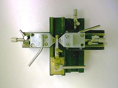
11 TEST FIXTURE
12
13
14
15
16
17
18
19
FERRITE DEVICES CONTENTS CIRCULATORS & ISOLATORS SPECIFIC REQUEST TECHNICAL INFORMATION DROP-IN CIRCULATORS & ISOLATORS...
 FERRITE DEVICES CONTENTS PAGE CIRCULATORS & ISOLATORS SPECIFIC REQUEST........................ 75 TECHNICAL INFORMATION...................................................... 76 DROP-IN CIRCULATORS & ISOLATORS......................................
Circulator Construction
 ISOLATORS pg. 1 UNDERSTANDING COAXIAL AND DROP-IN CIRCULATORS AND ISOLATORS This article describes the basic operating principles of the stripline junction circulator. The following information has been
MICROWAVE MICROWAVE TRAINING BENCH COMPONENT SPECIFICATIONS:
 Microwave section consists of Basic Microwave Training Bench, Advance Microwave Training Bench and Microwave Communication Training System. Microwave Training System is used to study all the concepts of
CIRCULATOR APPLICATION NOTE ANV001.
 APPLICATION NOTE ANV001 Bötelkamp 31, D-22529 Hamburg, GERMANY Phone: +49-40 547 544 60 Fax: +49-40 547 544 666 Email: info@valvo.com A Circulator is defined as a non-reciprocal, passive three ports, ferromagnetic
Application Note 5525
 Using the Wafer Scale Packaged Detector in 2 to 6 GHz Applications Application Note 5525 Introduction The is a broadband directional coupler with integrated temperature compensated detector designed for
MICROWAVE AND RADAR LAB (EE-322-F) LAB MANUAL VI SEMESTER
 LAB MANUAL VI SEMESTER") 1 MICROWAVE AND RADAR LAB (EE-322-F) MICROWAVE AND RADAR LAB (EE-322-F) LAB MANUAL VI SEMESTER RAO PAHALD SINGH GROUP OF INSTITUTIONS BALANA(MOHINDERGARH)123029 Department Of Electronics and Communication
1 MICROWAVE AND RADAR LAB (EE-322-F) MICROWAVE AND RADAR LAB (EE-322-F) LAB MANUAL VI SEMESTER RAO PAHALD SINGH GROUP OF INSTITUTIONS BALANA(MOHINDERGARH)123029 Department Of Electronics and Communication
3. (a) Derive an expression for the Hull cut off condition for cylindrical magnetron oscillator. (b) Write short notes on 8 cavity magnetron [8+8]
![3. (a) Derive an expression for the Hull cut off condition for cylindrical magnetron oscillator. (b) Write short notes on 8 cavity magnetron [8+8]](/thumbs/73/68588725.jpg "3. (a) Derive an expression for the Hull cut off condition for cylindrical magnetron oscillator. (b) Write short notes on 8 cavity magnetron [8+8]") Code No: RR320404 Set No. 1 1. (a) Compare Drift space bunching and Reflector bunching with the help of Applegate diagrams. (b) A reflex Klystron operates at the peak of n=1 or 3 / 4 mode. The dc power
Code No: RR320404 Set No. 1 1. (a) Compare Drift space bunching and Reflector bunching with the help of Applegate diagrams. (b) A reflex Klystron operates at the peak of n=1 or 3 / 4 mode. The dc power
VSWR MEASUREMENT APPLICATION NOTE ANV004.
 APPLICATION NOTE ANV004 Bötelkamp 31, D-22529 Hamburg, GERMANY Phone: +49-40 547 544 60 Fax: +49-40 547 544 666 Email: info@valvo.com Introduction: VSWR stands for voltage standing wave ratio. The ratio
Design and Matching of a 60-GHz Printed Antenna
 Application Example Design and Matching of a 60-GHz Printed Antenna Using NI AWR Software and AWR Connected for Optenni Figure 1: Patch antenna performance. Impedance matching of high-frequency components
SMT Hybrid Couplers, RF Parameters and Applications
 SMT Hybrid Couplers, RF Parameters and Applications A 90 degree hybrid coupler is a four-port device used to equally split an input signal into two signals with a 90 degree phase shift between them. The
Many applications. Mismatched Load Characterization for High-Power RF Amplifiers PA CHARACTERIZATION. This article discusses the
 From April 2004 High Frequency Electronics Copyright 2004 Summit Technical Media, LLC Mismatched Load Characterization for High-Power RF Amplifiers By Richard W. Brounley, P.E. Brounley Engineering Many
GaAs MMIC devices are susceptible to Electrostatic Discharge. Use proper ESD precautions when handling these items.
 The is a broadband, power efficient GaAs PHEMT distributed amplifier in a 4mm QFN surface mount package. The is designed to provide optimal LO drive for T3 mixers. Typically, ADM-26-2931SM provides. db
100W Power Amplifier 8GHz~11GHz
 100W Power Amplifier 8GHz~11GHz High output power +50dBm Aerospace and military application X band radar High Peak to average handle capability All specifications can be modified upon request Parameter
SA18N-20 DATA SHEET. 20 db Fixed Attenuator N Male To N Female Up To 18 GHz Rated To 2 Watts With Passivated Stainless Steel Body.
 20 db Fixed Attenuator N Male To N Female Up To 18 GHz Rated To 2 Watts With Passivated Stainless Steel Body Fairview Microwave carries a broad selection of fixed attenuators with a wide range of attenuation
(a) The insertion loss is the average value of the transmission coefficient, S12 (db), in the passband (Figure 1 Label A)
 The insertion loss is the average value of the transmission coefficient, S12 (db), in the passband (Figure 1 Label A)") Lab 6-1: Microwave Multiport Circuits In this lab you will characterize several different multiport microstrip and coaxial components using a network analyzer. Some, but not all, of these components have
Lab 6-1: Microwave Multiport Circuits In this lab you will characterize several different multiport microstrip and coaxial components using a network analyzer. Some, but not all, of these components have
GaAs MMIC devices are susceptible to Electrostatic Discharge. Use proper ESD precautions when handling these items.
 ADM-26-931SM The ADM-26-931SM is a broadband, power efficient GaAs PHEMT distributed amplifier in a 4mm QFN surface mount package. The ADM-26-931SM is designed to provide optimal LO drive for T3 mixers.
Network Analysis Basics
 Adolfo Del Solar Application Engineer adolfo_del-solar@agilent.com MD1010 Network B2B Agenda Overview What Measurements do we make? Network Analyzer Hardware Error Models and Calibration Example Measurements
Measurements with Scattering Parameter By Joseph L. Cahak Copyright 2013 Sunshine Design Engineering Services
 Measurements with Scattering Parameter By Joseph L. Cahak Copyright 2013 Sunshine Design Engineering Services Network Analyzer Measurements In many RF and Microwave measurements the S-Parameters are typically
Return Loss Bridge Basics
 1.0 Introduction Return loss bridges have many useful applications for the two-way radio technician These bridges are particularly helpful when used with the tracking generator feature of many service
CHAPTER - 6 PIN DIODE CONTROL CIRCUITS FOR WIRELESS COMMUNICATIONS SYSTEMS
 CHAPTER - 6 PIN DIODE CONTROL CIRCUITS FOR WIRELESS COMMUNICATIONS SYSTEMS 2 NOTES 3 INTRODUCTION PIN DIODE CONTROL CIRCUITS FOR WIRELESS COMMUNICATIONS SYSTEMS Chapter 6 discusses PIN Control Circuits
Surface Mount PIN Diodes. Technical Data. HSMP-38XX and HSMP-48XX Series. Package Lead Code Identification. Features
 Surface Mount PIN Diodes Technical Data HSMP-38XX and HSMP-48XX Series Features Diodes Optimized for: Low Current Switching Low Distortion Attenuating Ultra-Low Distortion Switching Microwave Frequency
5W Ultra Wide Band Power Amplifier 2-18GHz. Parameter Min. Typ. Max. Min. Typ. Max. Units
 7-3 RF-LAMBDA 5W Ultra Wide Band Power Amplifier 2-18GHz Features Wideband Solid State Power Amplifier Psat: + 37dBm Gain: 35 db Supply Voltage: +24V Electrical Specifications, T A = +25⁰C, Vcc = +24V
8W Wide Band Power Amplifier 1GHz~22GHz
 8W Wide Band Power Amplifier 1GHz~22GHz Features Wideband Solid State Power Amplifier Gain: 50 db Typical Psat: +39 dbm Supply Voltage: +36V Electrical Specifications, T A = +25⁰C Typical Applications
Limiter Diodes Features Description Chip Dimensions Model DOT Diameter (Typ.) Chip Number St l Style Inches 4 11
 Chip Number St l Style Inches 4 11") Features Low Loss kw Coarse Limiters 200 Watt Midrange Limiters 10 mw Clean Up Limiters 210 20 Description Alpha has pioneered the microwave limiter diode. Because all phases of manufacturing, from design
Features Low Loss kw Coarse Limiters 200 Watt Midrange Limiters 10 mw Clean Up Limiters 210 20 Description Alpha has pioneered the microwave limiter diode. Because all phases of manufacturing, from design
Vector Network Analyzer
 Vector Network Analyzer VNA Basics VNA Roadshow Budapest 17/05/2016 Content Why Users Need VNAs VNA Terminology System Architecture Key Components Basic Measurements Calibration Methods Accuracy and Uncertainty
9W Power Amplifier 26.2GHz~34GHz
 9W Power Amplifier 26.2GHz~34GHz High output power > +39.5 dbm Aerospace and military application High Peak to average handle capability High Linearity and low noise figure All specifications can be modified
Combined Band MHz. Fig. 1 Typical Diplexer Filter Combiner Fig. 2 Typical Diplexer Combiner
 Choosing the Best Power Divider for the Task of Signal Combining As systems become more and more complex, choosing how best to combine two or more RF signals has become a far more difficult question to
30W Solid State High Power Amplifier 2-6 GHz. Parameter Min. Typ. Max. Min. Typ. Max. Units
 7-3 RF-LAMBDA 30W Solid State High Power Amplifier 2-6 GHz Features Wideband Solid State Power Amplifier Psat: +45dBm Gain: 50dB Supply Voltage: +36V Electrical Specifications, T A = +25⁰C, Vcc = +36V
High Power, Magnet-free, Waveguide Based Circulator Using Angular-Momentum Biasing of a Resonant Ring
 SLAC-R-1080 High Power, Magnet-free, Waveguide Based Circulator Using Angular-Momentum Biasing of a Resonant Ring Jeffrey Neilson and Emilio Nanni August 18, 2017 Prepared for Calabazas Creek Research,
Parameter Min. Typ. Max. Min. Typ. Max. Units
 25W Wide Band Power Amplifier 20-6000MHz Features Wideband Solid State Power Amplifier Psat: +45dBm Typical Gain: 50dB Typical Supply Voltage: +60V DC Electrical Specifications, T A =25 Parameter Min.
CAVITY TUNING. July written by Gary Moore Telewave, Inc. 660 Giguere Court, San Jose, CA Phone:
 CAVITY TUNING July 2017 -written by Gary Moore Telewave, Inc 660 Giguere Court, San Jose, CA 95133 Phone: 408-929-4400 1 P a g e Introduction Resonant coaxial cavities are the building blocks of modern
GaAs MMIC devices are susceptible to Electrostatic Discharge. Use proper ESD precautions when handling these items.
 ADM-12-931SM The ADM-12-931SM is a small, low power, and economical T3 driver or T3A pre-amplifier. It is a GaAs PHEMT distributed amplifier in a 3mm QFN surface mount package. The ADM-12-931SM can provide
SMA Self-Fixture End Launch Connectors
 SMA Self-Fixture End Launch Connectors INTRODUCTION / APPLICATIONS Applications for these connectors include: An ideal solution for design engineers who are obligated to cut manufacturing costs and complexity
Investigation of the Double-Y Balun for Feeding Pulsed Antennas
 Proceedings of the SPIE, Vol. 5089, April 2003 Investigation of the Double-Y Balun for Feeding Pulsed Antennas Jaikrishna B. Venkatesan a and Waymond R. Scott, Jr. b Georgia Institute of Technology Atlanta,
CHAPTER - 3 PIN DIODE RF ATTENUATORS
 CHAPTER - 3 PIN DIODE RF ATTENUATORS 2 NOTES 3 PIN DIODE VARIABLE ATTENUATORS INTRODUCTION An Attenuator [1] is a network designed to introduce a known amount of loss when functioning between two resistive
20W Solid State Power Amplifier 26.2GHz~34GHz. Parameter Min. Typ. Max. Min. Typ. Max. Units. Frequency Range GHz.
 20W Solid State Power Amplifier 26.2GHz~34GHz Features Wideband Solid State Power Amplifier Gain: 65dB Typical Psat: +43dBm Typical Supply : +24V Electrical Specifications, T A = +25⁰C, Vcc = +24V Typical
433 & 443 Series INTELLIGENT RELAY SP3T & SP4T IN-LINE Multithrow Switches
 433 & 443 Series INTELLIGENT RELAY SP3T & SP4T IN-LINE Multithrow Switches Available with two types of internal drive electronics (Binary Decoding or MOSFET Pulse Latching), these SP3T and SP4T IN-LINE
ELEC4604. RF Electronics. Experiment 2
 ELEC4604 RF Electronics Experiment MICROWAVE MEASUREMENT TECHNIQUES 1. Introduction and Objectives In designing the RF front end of a microwave communication system it is important to appreciate that the
EC 1402 Microwave Engineering
 SHRI ANGALAMMAN COLLEGE OF ENGINEERING & TECHNOLOGY (An ISO 9001:2008 Certified Institution) SIRUGANOOR,TRICHY-621105. DEPARTMENT OF ELECTRONICS AND COMMUNICATION ENGINEERING EC 1402 Microwave Engineering
MICROWAVE ENGINEERING-II. Unit- I MICROWAVE MEASUREMENTS
 MICROWAVE ENGINEERING-II Unit- I MICROWAVE MEASUREMENTS 1. Explain microwave power measurement. 2. Why we can not use ordinary diode and transistor in microwave detection and microwave amplification? 3.
HMPP-386x Series MiniPak Surface Mount RF PIN Diodes
 HMPP-86x Series MiniPak Surface Mount RF PIN Diodes Data Sheet Description/Applications These ultra-miniature products represent the blending of Avago Technologies proven semiconductor and the latest in
4W Ultra Wide Band Power Amplifier 0.1GHz~22GHz
 4W Ultra Wide Band Power Amplifier 0.1GHz~22GHz Features Wideband Solid State Power Amplifier Gain: 40 db Typical Psat: +37 dbm Typical Noise Figure: 3dB Typical Supply Voltage: +24V (-NP) / +36V (-WP)
GaAs MMIC devices are susceptible to Electrostatic Discharge. Use proper ESD precautions when handling these items.
 ADM-26-929SM The ADM-26-929SM is a broadband, efficient GaAs PHEMT distributed amplifier in a 4mm QFN surface mount package. It is designed to provide optimal LO drive for T3 mixers and offers 13 db typical
DEVELOPMENT AND PRODUCTION OF HYBRID CIRCUITS FOR MICROWAVE RADIO LINKS
 Electrocomponent Science and Technology 1977, Vol. 4, pp. 79-83 (C)Gordon and Breach Science Publishers Ltd., 1977 Printed in Great Britain DEVELOPMENT AND PRODUCTION OF HYBRID CIRCUITS FOR MICROWAVE RADIO
Microwave Fundamentals A Survey of Microwave Systems and Devices p. 3 The Relationship of Microwaves to Other Electronic Equipment p.
 Microwave Fundamentals A Survey of Microwave Systems and Devices p. 3 The Relationship of Microwaves to Other Electronic Equipment p. 3 Microwave Systems p. 5 The Microwave Spectrum p. 6 Why Microwave
PA FAN PLATE ASSEMBLY 188D6127G1 SYMBOL PART NO. DESCRIPTION. 4 SBS /10 Spring nut. 5 19A702339P510 Screw, thread forming, flat head.
 MAINTENANCE MANUAL 851-870 MHz, 110 WATT POWER AMPLIFIER 19D902797G5 TABLE OF CONTENTS Page DESCRIPTION.............................................. Front Page SPECIFICATIONS.................................................
100W Wide Band Power Amplifier 6GHz~18GHz. Parameter Min. Typ. Max. Min. Typ. Max. Units. Frequency Range GHz Gain db
 100W Wide Band Power Amplifier 6GHz~18GHz Features Wideband Solid State Power Amplifier Psat: +50dBm Gain: 75 db Typical Supply Voltage: +48V On board microprocessor driven bias controller. Electrical
MAHAVEER INSTITUTE OF SCIENCE & TECHNOLOGY. Microwave and Digital Communications Lab. Department Of Electronics and Communication Engineering
 MAHAVEER INSTITUTE OF SCIENCE & TECHNOLOGY Microwave and Digital Communications Lab Department Of Electronics and Communication Engineering MICROWAVE ENGINEERING LAB List of Experiments: 1.Reflex Klystron
50 W High Power Silicon PIN Diode SPDT Switch By Rick Puente, Skyworks Solutions, Inc.
 February 2012 50 W High Power Silicon PIN Diode SPDT Switch By Rick Puente, Skyworks Solutions, Inc. Radio transceiver designers have searched for a low cost solution to replace expensive mechanical switches
ECEN 5014, Spring 2009 Special Topics: Active Microwave Circuits Zoya Popovic, University of Colorado, Boulder
 ECEN 5014, Spring 2009 Special Topics: Active Microwave Circuits Zoya opovic, University of Colorado, Boulder LECTURE 3 MICROWAVE AMLIFIERS: INTRODUCTION L3.1. TRANSISTORS AS BILATERAL MULTIORTS Transistor
RESISTIVE POWER SPLITTERS AND DIVIDERS
 RESISTIVE POWER SPLITTERS AND DIVIDERS DC 40.0 GHz S Resistive Power Splitters Usage: : Use in RF and wireless applications where one of the two outputs are included in a leveling loop or used as a reference
Electrical Design of Narrow Band Filters. Giuseppe Macchiarella Polytechnic of Milan, Italy Electronic and Information Department
 Electrical Design of Narrow Band Filters Giuseppe Macchiarella Polytechnic of Milan, Italy Electronic and Information Department Introduction The design of a narrow band microwave filter starts with the
DC-20 GHz Distributed Driver Amplifier. Parameter Min Typ Max Min Typ Max Units
 7-3 RF-LAMBDA DC-20 GHz Distributed Driver Amplifier Electrical Specifications, T A =25 Features Ultra wideband performance Positive gain slope High output power Low noise figure Microwave radio and VSAT
MA4L Series. Silicon PIN Limiters RoHS Compliant. M/A-COM Products Rev. V12. Features. Chip Outline. Description. Applications
 Features Low Insertion Loss and Noise Figure High Peak and Average Operating Power Various P1dB Compression Powers Low Flat Leakage Power Proven Reliable, Silicon Nitride Passivation Chip Outline A Square
SA26B-10 DATA SHEET. 10 db Fixed Attenuator SMA Male To SMA Female Up To 26 GHz Rated To 2 Watts With Passivated Stainless Steel Body.
 10 db Fixed Attenuator SMA Male To SMA Female Up To 26 GHz Rated To 2 Watts With Passivated Stainless Steel Body Fairview Microwave carries a broad selection of fixed attenuators with a wide range of attenuation
Understanding Power Splitters
 Understanding Power Splitters How they work, what parameters are critical, and how to select the best value for your application. Basically, a 0 splitter is a passive device which accepts an input signal
PAGE 1/6 ISSUE SERIES Micro-SPDT PART NUMBER R516 XXX 10X. (All dimensions are in mm [inches]) R 516 _ 1 0 _
![PAGE 1/6 ISSUE SERIES Micro-SPDT PART NUMBER R516 XXX 10X. (All dimensions are in mm [inches]) R 516 _ 1 0 _](/thumbs/96/127769340.jpg "PAGE 1/6 ISSUE SERIES Micro-SPDT PART NUMBER R516 XXX 10X. (All dimensions are in mm [inches]) R 516 _ 1 0 _") PAGE 1/6 ISSUE 15-10-18 SERIES Micro-SPDT PART NUMBER R516 XXX 10X R516 series: the RAMSES concept merges with the SLIM LINE technology, breaking up the frequency limits of SMT switches : - FULL SMT TECHNOLOGY
PAGE 1/6 ISSUE 15-10-18 SERIES Micro-SPDT PART NUMBER R516 XXX 10X R516 series: the RAMSES concept merges with the SLIM LINE technology, breaking up the frequency limits of SMT switches : - FULL SMT TECHNOLOGY
CHAPTER 4. Practical Design
 CHAPTER 4 Practical Design The results in Chapter 3 indicate that the 2-D CCS TL can be used to synthesize a wider range of characteristic impedance, flatten propagation characteristics, and place passive
R.K.YADAV. 2. Explain with suitable sketch the operation of two-cavity Klystron amplifier. explain the concept of velocity and current modulations.
 Question Bank DEPARTMENT OF ELECTRONICS AND COMMUNICATION SUBJECT- MICROWAVE ENGINEERING(EEC-603) Unit-III 1. What are the high frequency limitations of conventional tubes? Explain clearly. 2. Explain
27-31 GHz 2W Balanced Power Amplifier TGA4513-CP
 27-31 GHz 2W Balanced Power Amplifier Key Features 27-31 GHz Bandwidth > 32 dbm Nominal P1dB 33 dbm Nominal Psat 22 db Nominal Gain IMD3 is 32 dbc @ 18 dbm SCL 12 db Nominal Return Loss Bias: 6 V, 84 ma
Intermodulation Distortion in RF Connectors
 Intermodulation Distortion in RF Connectors Introduction Intermodulation distortion or IMD has always existed in RF transmission paths. Until about the early 1990 s, cellular communications had relatively
Dinesh Micro Waves & Electronics
 Wave Guide Components RECTANGULAR WAVE GUDES Dinesh Microwaves and Electronics manufacturers of high power waveguide in the microwaves industry, this experience had resulted in designing, manufacturing
PUSH-PUSH DIELECTRIC RESONATOR OSCILLATOR USING SUBSTRATE INTEGRATED WAVEGUIDE POW- ER COMBINER
 Progress In Electromagnetics Research Letters, Vol. 30, 105 113, 2012 PUSH-PUSH DIELECTRIC RESONATOR OSCILLATOR USING SUBSTRATE INTEGRATED WAVEGUIDE POW- ER COMBINER P. Su *, Z. X. Tang, and B. Zhang School
PARAMETER CONDITIONS TYPICAL PERFORMANCE Operating Supply Voltage 3.1V to 3.5V Supply Current V CC = 3.3V, LO applied 152mA
 DESCRIPTION LT5578 Demonstration circuit 1545A-x is a high linearity upconverting mixer featuring the LT5578. The LT 5578 is a high performance upconverting mixer IC optimized for output frequencies in
PAGE 1/6 ISSUE Jul SERIES Micro-SPDT PART NUMBER R516 XXX 10X R 516 _ 1 0 _
 PAGE 1/6 ISSUE Jul-24-2017 SERIES Micro-SPDT PART NUMBER R516 XXX 10X R516 series: the RAMSES concept merges with the SLIM LINE technology, breaking up the frequency limits of SMT switches : - FULL SMT
A HIGH-POWER LOW-LOSS MULTIPORT RADIAL WAVEGUIDE POWER DIVIDER
 Progress In Electromagnetics Research Letters, Vol. 31, 189 198, 2012 A HIGH-POWER LOW-LOSS MULTIPORT RADIAL WAVEGUIDE POWER DIVIDER X.-Q. Li *, Q.-X. Liu, and J.-Q. Zhang School of Physical Science and
BROADBAND DISTRIBUTED AMPLIFIER
 ADM-126-83SM The ADM-126-83SM is a broadband, efficient GaAs PHEMT distributed amplifier with an integrated bias tee in a 4mm QFN surface mount package, designed to provide efficient LO drive for T3 mixers.
Ultra Wide Band Low Noise Amplifier GHz. Electrical Specifications, TA = +25⁰C, With Vg= -5V, Vcc = +4V ~ +7V, 50 Ohm System
 Ultra Wide Band Low Noise Amplifier 0.5 46GHz Parameter Min. Typ. Max. Min. Typ. Max. Units Frequency Range 0.5 20 20 46 GHz Gain 13 13 db Gain Variation Over Temperature (-45 ~ +85) ±3 ±2 db Noise Figure
RFSWLM S-Band Switch Limiter Module
 PRELIMINARY RFSWLM-2420-131 S-Band Switch Limiter Module Features: Surface Mount S- Band Switch Limiter Module 5mm x 8mm x 2.5mm Frequency Range: 2 to 4 GHz Higher Average Power Handling than Plastic Packages
Practical Measurements of Dielectric Constant and Loss for PCB Materials at High Frequency
 8 th Annual Symposium on Signal Integrity PENN STATE, Harrisburg Center for Signal Integrity Practical Measurements of Dielectric Constant and Loss for PCB Materials at High Frequency Practical Measurements
For EECS142, Lecture presented by Dr. Joel Dunsmore. Slide 1 Welcome to Network Analyzer Basics.
 For EECS142, Lecture presented by Dr. Joel Dunsmore Slide 1 Welcome to Network Analyzer Basics. Slide 2 One of the most fundamental concepts of high-frequency network analysis involves incident, reflected
Surface Mount RF PIN Diodes. Technical Data. HSMP-383x Series. Features. Package Lead Code Identification (Top View)
") Surface Mount RF PIN Diodes Technical Data HSMP-383x Series Features Diodes Optimized for: Low Capacitance Switching Low Current Attenuator Surface Mount SOT-23 Package Single and Dual Versions Tape and
Surface Mount RF PIN Diodes Technical Data HSMP-383x Series Features Diodes Optimized for: Low Capacitance Switching Low Current Attenuator Surface Mount SOT-23 Package Single and Dual Versions Tape and
Configuration of PNA-X, NVNA and X parameters
 Configuration of PNA-X, NVNA and X parameters VNA 1. S-Parameter Measurements 2. Harmonic Measurements NVNA 3. X-Parameter Measurements Introducing the PNA-X 50 GHz 43.5 GHz 26.5 GHz 13.5 GHz PNA-X Agilent
Application Note AN-00502
 Proper PCB Design for Embedded Antennas Application Note AN-00502 Introduction Embedded antennas are ideal for products that cannot use an external antenna. The reasons for this can range from ergonomic
100W High Power Silicon PIN Diode SPDT Switches By Rick Puente, Skyworks Solutions, Inc.
 October 2013 100W High Power Silicon PIN Diode SPDT Switches By Rick Puente, Skyworks Solutions, Inc. Radio transceiver designers have searched for a low cost solution to replace expensive mechanical switches
Bill Ham Martin Ogbuokiri. This clause specifies the electrical performance requirements for shielded and unshielded cables.
 098-219r2 Prepared by: Ed Armstrong Zane Daggett Bill Ham Martin Ogbuokiri Date: 07-24-98 Revised: 09-29-98 Revised again: 10-14-98 Revised again: 12-2-98 Revised again: 01-18-99 1. REQUIREMENTS FOR SPI-3
Welcome to AntennaSelect Volume 1 August 2013
 Welcome to AntennaSelect Volume 1 August 2013 This is the first issue of our new periodic newsletter, AntennaSelect. AntennaSelect will feature informative articles about antennas and antenna technology,
Features. Output Third Order Intercept (IP3) [2] dbm Power Added Efficiency %
![Features. Output Third Order Intercept (IP3) [2] dbm Power Added Efficiency %](/thumbs/84/89186722.jpg "Features. Output Third Order Intercept (IP3) [2] dbm Power Added Efficiency %") v5.1217 HMC187 2-2 GHz Typical Applications The HMC187 is ideal for: Test Instrumentation General Communications Radar Functional Diagram Features High Psat: +39 dbm Power Gain at Psat: +5.5 db High Output
v5.1217 HMC187 2-2 GHz Typical Applications The HMC187 is ideal for: Test Instrumentation General Communications Radar Functional Diagram Features High Psat: +39 dbm Power Gain at Psat: +5.5 db High Output
20W Solid State Power Amplifier 6-18GHz. Parameter Min. Typ. Max. Min. Typ. Max. Units
 7-3 RF-LAMBDA 20W Solid State Power Amplifier 6-18GHz Electrical Specifications, TA = +25⁰C Vcc = +36V Features Psat: + 43.5dBm Gain: 51 db Supply Voltage: +36V 50 Ohm Matched Short Haul / High Capacity
Cell Extender Antenna System Design Guide Lines
 Cell Extender Antenna System Design Guide Lines 1. General The design of an Antenna system for a Cell Extender site needs to take into account the following specific factors: a) The systems input and output
Pin Connections and Package Marking. GUx
 Surface Mount RF PIN Switch Diodes Technical Data HSMP-389x Series HSMP-89x Series Features Unique Configurations in Surface Mount Packages Add Flexibility Save Board Space Reduce Cost Switching Low Capacitance
FieldFox Handheld Education Series Part 3: Calibration Techniques for Precise Field Measurements
 FieldFox Handheld Education Series Part 3: Calibration Techniques for Precise Field Measurements FieldFox Handheld Education Series Interference Testing Cable and Antenna Measurements Calibration Techniques
MMIC GHz Quadrature Hybrid
 MMIC 3.5-10GHz Quadrature Hybrid MQH-3R510 1 Device Overview 1.1 General Description The MQH-3R510 is a MMIC 3.5 GHz 10 GHz quadrature (90 ) hybrid. Wire bondable 50Ω terminations are available on-chip.
Exercise 3-2. Effects of Attenuation on the VSWR EXERCISE OBJECTIVES
 Exercise 3-2 Effects of Attenuation on the VSWR EXERCISE OBJECTIVES Upon completion of this exercise, you will know what the attenuation constant is and how to measure it. You will be able to define important
ECE 4265/6265 Laboratory Project 7 Network Analyzer Calibration
 ECE 4265/6265 Laboratory Project 7 Network Analyzer Calibration Objectives The purpose of this lab is to introduce the concepts of calibration and error correction for microwave s-parameter measurements.
Description and Laboratory Evaluation of a Prototype LMR Multiband Antenna System
 Description and Laboratory Evaluation of a Prototype LMR Multiband Antenna System Steve Ellingson September 20, 2010 Contents 1 Introduction 2 2 Design 2 3 Performance 2 Bradley Dept. of Electrical & Computer
Gallium Nitride MMIC Power Amplifier
 Gallium Nitride MMIC Power Amplifier August 2015 Rev 4 DESCRIPTION AMCOM s is an ultra-broadband GaN MMIC power amplifier. It has 21dB gain, and >41dBm output power over the 0.03 to 6GHz band. This MMIC
Isolators & Loads. You re heard, loud and clear.
 Isolators & Loads You re heard, loud and clear. isolators, Circulators & loads 118-960 MHz Bird Technologies group, TX rx systems brand, isolators are designed to provide the specified isolation under
Exercise problems of topic 1: Transmission line theory and typical waveguides
 Exercise problems of topic 1: Transmission line theory and typical waveguides Return your answers in the contact sessions on a paper; either handwritten or typescripted. You can return them one by one.
Swept Return Loss & VSWR Antenna Measurements using the Eagle Technologies RF Bridge
 Swept Return Loss & VSWR Antenna Measurements using the Eagle Technologies RF Bridge April, 2015 Page 1 of 7 Introduction Return loss and VSWR are a measure of the magnitude of a transmitted RF Signal
AMPLIFIERS, ANTENNAS, MULTIPLIERS, SOURCES, WAVEGUIDE PRODUCTS MILLIMETER-WAVE COMPONENTS FERRITE PRODUCTS AND SUB-SYSTEMS
 AMPLIFIERS, ANTENNAS, MULTIPLIERS, SOURCES, WAVEGUIDE PRODUCTS MILLIMETER-WAVE COMPONENTS FERRITE PRODUCTS AND SUB-SYSTEMS 766 San Aleso Avenue, Sunnyvale, C A 94085 Tel. (408) 541-9226, Fax (408) 541-9229
Application Note: Swept Return Loss & VSWR Antenna Measurements using the Eagle Technologies RF Bridge
 : Swept Return Loss & VSWR Antenna Measurements using the Eagle Technologies RF Bridge FCT-1008A Introduction Return loss and VSWR are a measure of the magnitude of a transmitted RF Signal in relation
dbm Supply Current (Idd) (Vdd=+36V)
 (Vdd=+36V)") Ka Band 6W Power Amplifier 28GHz~42GHz High output power Aerospace and military application High Peak to average handle capability High Linearity and low noise figure All specifications can be modified
Ka Band 6W Power Amplifier 28GHz~42GHz High output power Aerospace and military application High Peak to average handle capability High Linearity and low noise figure All specifications can be modified
Power Dividers and Directional Couplers (7)
") Microwave Circuits 1 Power Dividers and Directional Couplers (7) The T-Junction Power Divider(7.2) Lossless Divider 1. Lossless 2. Match at the input port. 3. Mismatch at the output ports. 4. No isolation
Microwave Circuits 1 Power Dividers and Directional Couplers (7) The T-Junction Power Divider(7.2) Lossless Divider 1. Lossless 2. Match at the input port. 3. Mismatch at the output ports. 4. No isolation
2W Ultra Wide Band Power Amplifier 0.2GHz~35GHz. Parameter Min. Typ. Max. Min. Typ. Max. Min. Typ. Max. Units. Frequency Range
 2W Ultra Wide Band Power Amplifier 0.2GHz~35GHz Features Wideband Solid State Power Amplifier Gain: 37dB Typical Psat 35dBm Typical Electrical Specifications, TA = +25⁰C, Vcc = +12V. Parameter Min. Typ.
Lecture 16 Microwave Detector and Switching Diodes
 Basic Building Blocks of Microwave Engineering Prof. Amitabha Bhattacharya Department of Electronics and Communication Engineering Indian Institute of Technology, Kharagpur Lecture 16 Microwave Detector
Hot S 22 and Hot K-factor Measurements
 Application Note Hot S 22 and Hot K-factor Measurements Scorpion db S Parameter Smith Chart.5 2 1 Normal S 22.2 Normal S 22 5 0 Hot S 22 Hot S 22 -.2-5 875 MHz 975 MHz -.5-2 To Receiver -.1 DUT Main Drive
HIGH REPEATABILITY, TO-5 RELAYS DPDT
 HIGH REPEATABILITY, TO-5 RELAYS DPDT SERIES RELAY TYPE RF7 RF7 Repeatable, RF relay Sensitive, repeatable, RF relay DESCRIPTION The ultraminiature RF7 and RF7 relays are designed to provide improved RF
Chapter 5 DESIGN AND IMPLEMENTATION OF SWASTIKA-SHAPED FREQUENCY RECONFIGURABLE ANTENNA ON FR4 SUBSTRATE
 Chapter 5 DESIGN AND IMPLEMENTATION OF SWASTIKA-SHAPED FREQUENCY RECONFIGURABLE ANTENNA ON FR4 SUBSTRATE The same geometrical shape of the Swastika as developed in previous chapter has been implemented
PRELIMINARY DATASHEET
 PRELIMINARY DATASHEET 8-12 GHz 41dBm Power Amplifier DESCRIPTION The is a high performance dual line-up 3 stages GaAs Power Amplifier MMIC designed to operate in the X band. The has an output power of