FYS 4340/FYS Diffraction Methods & Electron Microscopy. Lecture 3. Sandeep Gorantla. FYS 4340/9340 course Autumn
|
|
|
- Annice Golden
- 5 years ago
- Views:
Transcription

1 FYS 4340/FYS 9340 Diffraction Methods & Electron Microscopy Lecture 3 Sandeep Gorantla 63
2 Lab Groups THURSDAY TEM COURSE (FYS 4340/FYS 9340) LAB GROUPS PLAN Group 1 Group 2 Group 3 9:00-11:00 12:00-14:00 14:00-16:00 Annika Utz Amalie Berg Hans Jakob Sivertsen Mollatt Andrei Karzhou Nikita Thind Heine Ness Martin Løvøy Hengyi zhu Henrik Riis Martin Jensen/Anne Klemm PrasantaDhak 64

3 Simplified ray diagram of conventional TEM Simplified ray diagram of conventional STEM 65
4 This Lecture TEM Instrumentation Part 2 (Text book Chapters: 5 9) TEM Specimen Preparation (Text book Chapters: 10) 66


5 Electron gun Illumination system Specimen stage Imaging system Projection and Detection system Courtesy: David Rassouw 67
6 EELS prism FEG gun Extraction Anode Gun lens Monochromator Aperture Monochromator Accelerator Gun Shift coils C1 aperture/mono energy slit C1 lens C2 lens C2 aperture Condenser alignment coils C3 lens C3 aperture Beam shift coils Mini condenser lens Objective lens upper Specimen Stage Objective lens upper Image Shift coils Objective aperture Cs Corrector SA Aperture Diffraction lens Intermediate lens Projector 1 lens Projector 2 lens HAADF detector Viewing Chamber Phosphorous Screen BF/CCD detectors GIF CCD detector Electron Gun Electron Lens Apertures Stigmators, scan coils and beam deflecting coils Specimen Stage/Holders Lq. N 2 Coldtrap Image Viewing/Recording system Spectrometers Courtesy: David Rassouw, CCEM, Canada 68
7 The requirements of the illumination system High electron intensity Image visible at high magnifications Small energy spread Reduce chromatic aberrations effect in obj. lens High brightness of the electron beam Reduce spherical aberration effects in the obj. lens Adequate working space between the illumination system and the specimen 69


8 The electron source Two types of emission sources Thermionic emission W or LaB6 Field emission Cold FEG Schottky FEG W ZnO/W 70
9 The electron gun The performance of the gun is characterised by: Beam diameter, d cr Divergence angle, α cr Beam current, I cr d Cross over Beam brightness, β cr at the cross over α Image of source 71
10 Brightness Brightness is the current density per unit solid angle of the source β = i cr /(πd cr α cr ) 2 Beam diameter, d cr Divergence angle, α cr Beam current, I cr Beam brightness, β cr at the cross over 72
11 The electron gun FEG Thermionic gun Wehnelt cylinder Cathode -200 kv Bias -200 V Anode Equipotential lines Ground potential d cr Cross over α cr 73
12 Thermionic guns Filament heated to give Thermionic emission -Directly (W) or indirectly (LaB 6 ) Filament negative potential to ground Wehnelt produces a small negative bias -Brings electrons to cross over 74
13 Thermionic guns 75
14 Thermionic emission Current density: J c = A c T 2 exp(-φ c /kt) Richardson-Dushman Ac: Richardson s constant, material dependent T: Operating temperature (K) φ: Work function (natural barrier to prevent electrons to leak out from the surface) k: Boltzmann s constant Maximum usable temperature T is determined by the onset of the evaporation of material. 76

15 The principle: Field emission The strength of an electric field E is considerably increased at sharp points. E=V/r r W < 0.1 µm, V=1 kv E = V/m Lowers the work-function barrier so that electrons can tunnel out of the tungsten. Surface has to be pristine (no contamination or oxide) Ultra high vacuum condition (Cold FEG) or poorer vacuum if tip is heated ( thermal FE; ZrO surface tratments Schottky emitters). 77
16 Field emission Current density: Fowler-Norheim Maxwell-Boltzmann energy distribution for all sources 78
 100 20 100 20~100 Brightness B (A/m 2 sr) 5*10 9 5*10 10 5*10 12 5*10 12 Energy spread ΔE (ev) 2.3 1.5 0.6~0.8 0.3~0.")
17 Characteristics of principal electron sources at 200 kv W Thermionic LaB6 Thermionic FEG Schottky (ZrO/W) FEG cold (W) Current density J c (A/m 2 ) 2-3* *10 4 1*10 7 Electron source size (µm) Emission current (µa) ~100 Brightness B (A/m 2 sr) 5*10 9 5* * *10 12 Energy spread ΔE (ev) ~ ~0.7 Vacuum pressure (Pa)* Vacuum temperature (K) * Might be one order lower 79
18 Advantages and disadvantages of the different electron sources W Advantages: LaB 6 advantages: FEG advantages: Rugged and easy to handle High brightness Extremely high brightness Requires only moderat vacuum Good long time stability High total beam current High total beam current Long life time ( h) Long life time, more than 1000 h. W disadvantages: LaB 6 disadvantages: FEG disadvantages: Low brightness Fragile and delicate to handle Very fragile Limited life time (100 h) Requires better vacuum Current instabilities Long time instabilities Ultra high vacuum to remain stable 80
19 Electron lenses Any axially symmetrical electric or magnetic field have the properties of an ideal lens for paraxial rays of charged particles. Electrostatic Require high voltage- insulation problems F= -ee Not used as imaging lenses, but are used in modern monochromators ElectroMagnetic Can be made more accurately Shorter focal length F= -e(v x B) 81

20 General features of magnetic lenses Focus near-axis electron rays with the same accuracy as a glass lens focusses near axis light rays Same aberrations as glass lenses Converging lenses The bore of the pole pieces in an objective lens is about 4 mm or less A single magnetic lens rotates the image relative to the object Focal length can be varied by changing the field between the pole pieces. (Changing magnification) 82


21 Strengths of lenses and focused image of the source If you turn up one lens (i.e. make it stronger, or over- focus then you must turn the other lens down (i.e. make it weaker, or under-focus it, or turn its knob anti-clockwise) to keep the image in focus. 83
 of the two lenses are changed, the magnification of the image")
22 Magnification of image, Rays from different parts of the object If the strengths (excitations) of the two lenses are changed, the magnification of the image changes 84
23 Often a double or twin lens The Objective lens The most important lens Determines the reolving power of the TEM All the aberations of the objective lens are magnified by the intermediate and projector lens. The most important aberrations Asigmatism Spherical Chromatical 85
24 Stigmators Astigmatism Can be corrected for with stigmators 86
25 Stigmators 87

26 Apertures 88
27 Use of apertures Condenser aperture: Limit the beam divergence (reducing the diameter of the discs in the convergent electron diffraction pattern). Limit the number of electrons hitting the sample (reducing the intensity),. Objective aperture: Control the contrast in the image. Allow certain reflections to contribute to the image. Bright field imaging (central beam, 000), Dark field imaging (one reflection, g), High resolution Images (several reflections from a zone axis). Selected area aperture: Select diffraction patterns from small (> 1µm) areas of the specimen. Allows only electrons going through an area on the sample that is limited by the SAD aperture to contribute to the diffraction pattern (SAD pattern). 89
 Bright field (BF) Ag and Pb")

28 Objective aperture: Contrast enhancement hole glue (light elements) Bright field (BF) Ag and Pb Objective aperture Si BF image All electrons contributes to the image. Only central beam contributes to the image. 90
, dark field (DF) and")
 Objective aperture BF")


29 Small objective aperture Bright field (BF), dark field (DF) and weak-beam (WB) (Diffraction contrast) Objective aperture BF image DF image Weak-beam Dissociation of pure screw dislocation In Ni 3 Al, Meng and Preston, J. Mater. Scicence, 35, p ,
 HREM image Phase")
30 Large objective aperture High Resolution Electron Microscopy (HREM) HREM image Phase contrast 92
31 Selected Area Diffraction Aperture Parallel incoming electron beam Selected area diffraction Specimen with two crystals (red and blue) Objective lense Pattern on the screen Diffraction pattern Image plane Selected area aperture 93
32 Diffraction with no apertures Convergent beam and Micro diffraction (CBED and µ-diffraction) Convergent beam Focused beam C2 lens Convergent beam Illuminated area less than the SAD aperture size. Small probe CBED pattern Diffraction information from an area with ~ same thickness and crystal orientation µ-diffraction pattern 94
33 Shadow imaging (diffraction mode) Parallel incoming electron beam Sample Objective lense Diffraction plane (back focal plane) Image plane 95
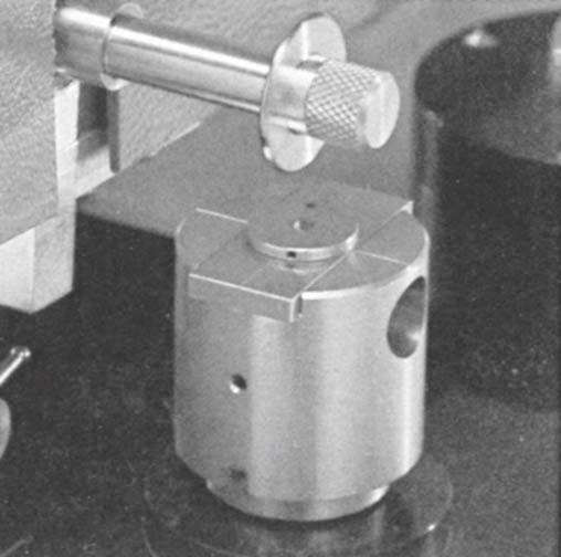
34 Specimen holders and goniometers Specimen holders Single tilt holders Double tilt holders Rotation holders Heating holders Up to 800 o C Cooling holders N: o C He: 4-10K Strain holders Environmental cells Goniometers: - Side-entry stage - Most common type - Eucentric - Top-entry stage - Less obj. lens aberrations - Not eucentric - Smaller tilting angles 96
35 Next Lecture TEM Specimen Preparation (Text book Chapters: 10) 97
36 Learning outcome HMS awareness Overview of common techniques Possible artifacts You should be able to evaluate which technique to use for a given sample Lab will give you some practical skills 98
37 What to consider before preparing a TEM specimen Ductile/fragile Bulk/surface/powder Insulating/conducting What is the objectiv of the Heat resistant TEM work? Irradiation resistant Single phase/multi phase Can mechanical damage be tolerated? Can chemical changes be accepted? Etc, etc. 99


38 Specimen preparation for TEM Crushing Cutting saw, diamond pen, ultrasonic drill, FIB Mechanical thinning Grinding, dimpling, Tripod polishing Electrochemical thinning Ion milling Coating Replica methods Etc. 100


39 SAFETY!!!! Know what you handling. MSDS Protect your self and others around you. Follow instructions If an accident occurs, know how to respond. 101
40 Safety rules Be sure that you can safely dispose of the waste product before you start. Be sure you have the antidote at hand. Never work alone in the specimenpreparation laboratory. Always wear safety glasses when preparing specimens and/or full protective clothing, including face masks and gloves, if so advised by the safety manual. Only make up enough of the solution for the one polishing session. Never use a mouth pipette for measuring any component of the solution. Dispose of the solution after use. Always work in a fume hood when using chemicals. Check that the extraction rate of the hood is sufficient for the chemical used. 102
41 Some acids for specimen preparation Cyanide solutions: DO NOT USE Perchloric acid in ethanol or methanol Ole Bjørn will make the solution if needed Nitric acid (HNO 3 ) Can produce explosive mixtures with ethanol. Hydrofluoric acid (HF) Penetrates flesh and dissolves bones rapidly! You need to have approval by supervisors and Ole Bjørn first! 103


42 Work in the Stucture Physics lab Get the local HMS instructions from Ole Bjørn Karlsen Ask Sign a form confirming that you have got the information 104
43 Preparation philosophy Self-supporting discs or specimen supported on a grid or washer 105
44 Self-supporting disk or grid Self supporting disk Consists of one material Can be a composite Can be handled with a tweeser Metallic, magnetic, nonmagnetic, plastic, vacuum If brittle, consider Cu washer with a slot Grid Several types (Fig. 10.3) Different materials (Cu, Ni ) Support brittle materials Support small particles The grid may contribute to the EDS. Common size: 3 mm. Smaller specimen diameters can be used for certain holders. 106

45 Grids and washers used as specimen support May contribute to the EDS signal. Common size: 3 mm. Smaller specimen diameters can be used for certain holders. 107
46 Preparation of self-supporting discs Cutting Ductile material or not? Grinding μm thick polish Cut the 3mm disc Dimple? Final thinning Ion beam milling Electropolishing 108
47 Self-supporting disk or grid Self supporting disk Consists of one material Can be a composite Can be handled with a tweeser Metallic, magnetic, nonmagnetic, plastic, vacuum Grid and washer Several types Different materials (Cu, Ni ) Support brittle materials Support small particles If brittle, consider Cu washer with a slot 109
48 Preparation of self-supporting discs Cutting/cleaving Ductile material or not? 110
49 Cutting and cleaving Cutting with a saw: Soft or brittle material? Brittle materials with well-defined cleavage plane Si GaAs NaCl MgO Razor blade or ultramicrotome 111
50 Preparation of self-supporting discs Cutting/cleaving Ductile material or not? Grinding μm thick polish Cut the 3mm disc 112

51 Cutting a 3 mm disc Soft or brittle material? Mechanical damage OK? Brittle: Spark erosion, ultrasonic drill, grinding drill 113
52 Preparation of self-supporting discs Cutting Ductile material or not? Grinding μm thick polish Cut the 3mm disc Prethinning Dimpling Tripod polishing 114

53 F Dimpling ΔΖ ω 115
54 Surface dimpling using a chemical solution Si: HF + HNO3 GaAs: Br + methanol The light pipe permits visual detection of perforation using the mirror. 116
55 Final thinning of the discs Electropolishing Ionmilling 117


56 Jet polishing Twin-jet electropolishing apparatus. The positively charged specimen is held in a Teflon holder between the jets. A light pipe (not shown) detects perforation and terminates the polishing. A single jet of gravity fed electrolyte thin a disk supported on a positively charged gauze. The disk has to be rotated periodically. 118

57 Ar ion beam thinning Variation in penetration depth and thinning rate with the angle of incidence. 119
 in")

58 Effect of Ar-thinning on CdTe Defects (dark spots) in Ar-thinned specimen Crystal thinned by reactive iodine ion milling. 120
59 Preparation of particles and fibers first embedding them in epoxy and forcing the epoxy into a 3-mm (outside) diameter brass tube prior to curing the epoxy. The tube and epoxy are then sectioned into disks with a diamond saw, dimpled, and ion milled to transparency. 121

60 THIN FILMS TEM specimen preparation Initial preparation steps Spacers : Si, glass, or some other inexpensive material. 122
61 THIN FILMS TEM specimen preparation Top view Cut out cylinder Grind down/ dimple Ione beam thinning Cut out slices Cut out a cylinder and glue it in a Cu-tube Grind down and glue on Cu-rings Cross section Glue the interface of interest face to face together with support material or Focused Ion Beam (FIB) Cut a slice of the cylinder and grind it down / dimple Cut off excess material Ione beam thinning 123
62 Electropolishing The window method Ultramicrotomy Crushing Specimens on grids/washers In ethanol Mix in an epoxy Replication and extraction Cleaving and SACT The 90 o wedge Lithography Preferensial chemical etching 124

63 Window polishing A sheet of the metal 100mm 2 is lacquered around the edges and made the anode of an electrolytic cell. Progress during thinning: the initial perforation usually occurs at the top of the sheet; lacquer is used to cover the initial perforation and the sheet is rotated 180 o and thinning continues to ensure that final thinning occurs near the center of the sheet. 125

64 Ultramicrotomy The sample is first embedded in epoxy or some other medium or the whole sample is clamped and moved across a knife edge. The thin flakes float off onto water or an appropriate inert medium, from where they are collected on grids. 126
 Evaporate a C, Cr, or Pt film onto the replicated plastic surface.")
65 Replication of a surface 1) Spray acetone on the surface to be replicated before pressing a plastic (usually cellulose acetate) 2) Removed the plastic from the surface when hardened 3) Evaporate a C, Cr, or Pt film onto the replicated plastic surface. 4) Dissolve the plastic with acetone Alternatively: the direct carbon replica. 127


66 Extraction replication A thin amorphous carbon film is evaporated over the particles The rest of the matrix is etched 128

67 Cleaving 1) Use tape 2) Dissolve tape in a solvent Cleaved MoS 2 showing regions of different shades of green, which correspond to different thicknesses. 129

68 SACT The small-angle cleaving technique Invaluable for films on Si or glass where there is no crystal structure 1. Scratch the sample; 2. Cleaving along the scratch; 130
 Mount the 90 o corner")
69 LACT- The 90 o wedge 1) Prethin: 2-mm square of the multilayers on a Si substrate 2) Scribe the Si through the surface layers, turn over, and cleave Need: a sharp 90 o edge; 3) Mount the 90 o corner 131

70 Preferential chemical etching Etch away most of the sample, leaving a small etched plateau Mask a region <50 nm across and etch away the majority of the surrounding plateau. Turn 90o and mounted in a specimen holder 132


71 Lithographic techniques Etching between the barrier layers Produces an undercutting down to the implanted layer which acts as an etch stop, producing a uniform layer 10 mm thick. 133


72 FIB Schematic of a two-beam (electron and ion) FIB instrument. -The area of interest has been marked. -A Pt bar is deposited to protect this area from the Ga beam. -The two trenches are cut. -The bottom and sides of the slice are (final) cut. -The TEM specimen is polished in place before extracting it. 134

73 A dual-beam FIB instrument. 135
74 Summary flow chart for specimen preparation 136

75 THERE WILL BE TEM COURSE LAB THIS THURSDAY *** Next Lecture Introduction to Crystallography by Patricia Almeida Carvalho Senior Research Scientist SINTEF 137
Transmissions Electron Microscopy (TEM)
") Transmissions Electron Microscopy (TEM) Basic principles Diffraction Imaging Specimen preparation A.E. Gunnæs MENA3100 V17 TEM is based on three possible set of techniqes Diffraction From regions down
Transmissions Electron Microscopy (TEM) Basic principles Diffraction Imaging Specimen preparation A.E. Gunnæs MENA3100 V17 TEM is based on three possible set of techniqes Diffraction From regions down
Scanning electron microscope
 Scanning electron microscope 6 th CEMM workshop Maja Koblar, Sc. Eng. Physics Outline The basic principle? What is an electron? Parts of the SEM Electron gun Electromagnetic lenses Apertures Chamber and
Transmission Electron Microscopy 9. The Instrument. Outline
 Transmission Electron Microscopy 9. The Instrument EMA 6518 Spring 2009 02/25/09 Outline The Illumination System The Objective Lens and Stage Forming Diffraction Patterns and Images Alignment and Stigmation
Chapter 2 Instrumentation for Analytical Electron Microscopy Lecture 7. Chapter 2 CHEM Fall L. Ma
 Chapter 2 Instrumentation for Analytical Electron Microscopy Lecture 7 Outline Electron Sources (Electron Guns) Thermionic: LaB 6 or W Field emission gun: cold or Schottky Lenses Focusing Aberration Probe
Scanning electron microscope
 Scanning electron microscope 5 th CEMM workshop Maja Koblar, Sc. Eng. Physics Outline The basic principle? What is an electron? Parts of the SEM Electron gun Electromagnetic lenses Apertures Detectors
2.Components of an electron microscope. a) vacuum systems, b) electron guns, c) electron optics, d) detectors. Marco Cantoni 021/
 vacuum systems, b) electron guns, c) electron optics, d) detectors. Marco Cantoni 021/") 2.Components of an electron microscope a) vacuum systems, b) electron guns, c) electron optics, d) detectors, 021/693.48.16 Centre Interdisciplinaire de Microscopie Electronique CIME Summary Electron propagation
2.Components of an electron microscope a) vacuum systems, b) electron guns, c) electron optics, d) detectors, 021/693.48.16 Centre Interdisciplinaire de Microscopie Electronique CIME Summary Electron propagation
p q p f f f q f p q f NANO 703-Notes Chapter 5-Magnification and Electron Sources
 Chapter 5-agnification and Electron Sources Lens equation Let s first consider the properties of an ideal lens. We want rays diverging from a point on an object in front of the lens to converge to a corresponding
Introduction of New Products
 Field Emission Electron Microscope JEM-3100F For evaluation of materials in the fields of nanoscience and nanomaterials science, TEM is required to provide resolution and analytical capabilities that can
S200 Course LECTURE 1 TEM
 S200 Course LECTURE 1 TEM Development of Electron Microscopy 1897 Discovery of the electron (J.J. Thompson) 1924 Particle and wave theory (L. de Broglie) 1926 Electromagnetic Lens (H. Busch) 1932 Construction
Tecnai on-line help manual --
 Tecnai on-line help Alignments 1 Tecnai on-line help manual -- Alignments Table of Contents 1 Alignments in the Tecnai microscope...5 2 Alignment procedures...6 3 Introduction to electron optics...11 3.1
MSE 460 TEM Lab 2: Basic Alignment and Operation of Microscope
 MSE 460 TEM Lab 2: Basic Alignment and Operation of Microscope Last updated on 1/8/2018 Jinsong Wu, jinsong-wu@northwestern.edu Aims: The aim of this lab is to familiarize you with basic TEM alignment
Introduction: Why electrons?
 Introduction: Why electrons? 1 Radiations Visible light X-rays Electrons Neutrons Advantages Not very damaging Easily focused Eye wonderful detector Small wavelength (Angstroms) Good penetration Small
ELECTRON MICROSCOPY. 13:10 16:00, Oct. 6, 2008 Institute of Physics, Academia Sinica. Tung Hsu
 ELECTRON MICROSCOPY 13:10 16:00, Oct. 6, 2008 Institute of Physics, Academia Sinica Tung Hsu Department of Materials Science and Engineering National Tsing Hua University Hsinchu 300, TAIWAN Tel. 03-5742564
Full-screen mode Popup controls. Overview of the microscope user interface, TEM User Interface and TIA on the left and EDS on the right
 Quick Guide to Operating FEI Titan Themis G2 200 (S)TEM: TEM mode Susheng Tan Nanoscale Fabrication and Characterization Facility, University of Pittsburgh Office: M104/B01 Benedum Hall, 412-383-5978,
NANO 703-Notes. Chapter 9-The Instrument
 1 Chapter 9-The Instrument Illumination (condenser) system Before (above) the sample, the purpose of electron lenses is to form the beam/probe that will illuminate the sample. Our electron source is macroscopic
TEM theory Basic optics, image formation and key elements
 Workshop series of Chinese 3DEM community Get acquainted with Cryo-Electron Microscopy: First Chinese Workshop for Structural Biologists TEM theory Basic optics, image formation and key elements Jianlin
Electron Sources, Optics and Detectors
 Thomas LaGrange, Ph.D. Faculty Lecturer and Senior Staff Scientist Electron Sources, Optics and Detectors TEM Doctoral Course MS-637 April 16 th -18 th, 2018 Summary Electron propagation is only possible
Scanning Electron Microscopy Basics and Applications
 Scanning Electron Microscopy Basics and Applications Dr. Julia Deuschle Stuttgart Center for Electron Microscopy MPI for Solid State Research Room: 1E15, phone: 0711/ 689-1193 email: j.deuschle@fkf.mpg.de
MODULE I SCANNING ELECTRON MICROSCOPE (SEM)
") MODULE I SCANNING ELECTRON MICROSCOPE (SEM) Scanning Electron Microscope (SEM) Initially, the plan of SEM was offered by H. Stintzing in 1927 (a German patent application). His suggested procedure was
MODULE I SCANNING ELECTRON MICROSCOPE (SEM) Scanning Electron Microscope (SEM) Initially, the plan of SEM was offered by H. Stintzing in 1927 (a German patent application). His suggested procedure was
2.Components of an electron microscope. a) vacuum systems, b) electron guns, c) electron optics, d) detectors. Marco Cantoni, 021/
 vacuum systems, b) electron guns, c) electron optics, d) detectors. Marco Cantoni, 021/") 2.Components of an electron microscope a) vacuum systems, b) electron guns, c) electron optics, d) detectors Marco Cantoni, 021/693.48.16 Centre Interdisciplinaire de Microscopie Electronique CIME MSE-603
2.Components of an electron microscope a) vacuum systems, b) electron guns, c) electron optics, d) detectors Marco Cantoni, 021/693.48.16 Centre Interdisciplinaire de Microscopie Electronique CIME MSE-603
Transmissions Electron Microscopy (TEM)
") Transmissions Electron Microscopy (TEM) Basic principles Diffraction Imaging Specimen preparation A.E. Gunnæs MENA3100 V18 Electron interaction with the (thin) specimen e - Typical specimen thickness Absorbed
Transmissions Electron Microscopy (TEM) Basic principles Diffraction Imaging Specimen preparation A.E. Gunnæs MENA3100 V18 Electron interaction with the (thin) specimen e - Typical specimen thickness Absorbed
SCANNING ELECTRON MICROSCOPY AND X-RAY MICROANALYSIS
 SCANNING ELECTRON MICROSCOPY AND X-RAY MICROANALYSIS Robert Edward Lee Electron Microscopy Center Department of Anatomy and Neurobiology Colorado State University P T R Prentice Hall, Englewood Cliffs,
ELECTRON MICROSCOPY. 14:10 17:00, Apr. 3, 2007 Department of Physics, National Taiwan University. Tung Hsu
 ELECTRON MICROSCOPY 14:10 17:00, Apr. 3, 2007 Department of Physics, National Taiwan University Tung Hsu Department of Materials Science and Engineering National Tsinghua University Hsinchu 300, TAIWAN
--> Buy True-PDF --> Auto-delivered in 0~10 minutes. JY/T
 Translated English of Chinese Standard: JY/T011-1996 www.chinesestandard.net Sales@ChineseStandard.net INDUSTRY STANDARD OF THE JY PEOPLE S REPUBLIC OF CHINA General rules for transmission electron microscopy
Basic Users Manual for Tecnai-F20 TEM
 Basic Users Manual for Tecnai-F20 TEM NB: This document contains my personal notes on the operating procedure of the Tecnai F20 and may be used as a rough guide for those new to the microscope. It may
Scanning Electron Microscopy. EMSE-515 F. Ernst
 Scanning Electron Microscopy EMSE-515 F. Ernst 1 2 Scanning Electron Microscopy Max Knoll Manfred von Ardenne Manfred von Ardenne Principle of Scanning Electron Microscopy 3 Principle of Scanning Electron
1.3. Before loading the holder into the TEM, make sure the X tilt is set to zero and the goniometer locked in place (this will make loading easier).
.") JEOL 200CX operating procedure Nicholas G. Rudawski ngr@ufl.edu (805) 252-4916 1. Specimen loading 1.1. Unlock the TUMI system. 1.2. Load specimen(s) into the holder. If using the double tilt holder, ensure
JEOL 200CX operating procedure Nicholas G. Rudawski ngr@ufl.edu (805) 252-4916 1. Specimen loading 1.1. Unlock the TUMI system. 1.2. Load specimen(s) into the holder. If using the double tilt holder, ensure
2. Raise HT to 200kVby following the procedure explained in 1.6.
 JEOL 2100 MANUAL Quick check list 1. If needed, fill the reservoir with LN2 2. Raise HT to 200kVby following the procedure explained in 1.6. 3. Insert specimen holder into TEM (Insert holder in airlock,
Transmission electron Microscopy
 Transmission electron Microscopy Image formation of a concave lens in geometrical optics Some basic features of the transmission electron microscope (TEM) can be understood from by analogy with the operation
Introduction to Transmission Electron Microscopy (Physical Sciences)
") Introduction to Transmission Electron Microscopy (Physical Sciences) Centre for Advanced Microscopy Program 9:30 10:45 Lecture 1 Basics of TEM 10:45 11:00 Morning tea 11:00 12:15 Lecture 2 Diffraction
Introduction to Transmission Electron Microscopy (Physical Sciences) Centre for Advanced Microscopy Program 9:30 10:45 Lecture 1 Basics of TEM 10:45 11:00 Morning tea 11:00 12:15 Lecture 2 Diffraction
Basics of Light Microscopy and Metallography
 ENGR45: Introduction to Materials Spring 2012 Laboratory 8 Basics of Light Microscopy and Metallography In this exercise you will: gain familiarity with the proper use of a research-grade light microscope
NanoSpective, Inc Progress Drive Suite 137 Orlando, Florida
 TEM Techniques Summary The TEM is an analytical instrument in which a thin membrane (typically < 100nm) is placed in the path of an energetic and highly coherent beam of electrons. Typical operating voltages
CHAPTER TWO METALLOGRAPHY & MICROSCOPY
 CHAPTER TWO METALLOGRAPHY & MICROSCOPY 1. INTRODUCTION: Materials characterisation has two main aspects: Accurately measuring the physical, mechanical and chemical properties of materials Accurately measuring
MSE 595T Transmission Electron Microscopy. Laboratory III TEM Imaging - I
 MSE 595T Basic Transmission Electron Microscopy TEM Imaging - I Purpose The purpose of this lab is to: 1. Make fine adjustments to the microscope alignment 2. Obtain a diffraction pattern 3. Obtain an
Indiana University JEM-3200FS
 Indiana University JEM-3200FS Installation Specification Model: JEM 3200FS Serial Number: EM 15000013 Objective Lens Configuration: High Resolution Pole Piece (HRP) JEOL Engineer: Michael P. Van Etten
This document assumes the user is already familiar with basic operation of the instrument in TEM mode and use of the Microscope Control interface.
 FEI Tecnai F20 S/TEM: imaging in STEM mode Nicholas G. Rudawski ngr@ufl.edu (805) 252-4916 (352) 392-3077 Last updated: 05/10/18 This document assumes the user is already familiar with basic operation
Chapter 4 Imaging Lecture 17
 Chapter 4 Imaging Lecture 17 d (110) Imaging Imaging in the TEM Diffraction Contrast in TEM Image HRTEM (High Resolution Transmission Electron Microscopy) Imaging STEM imaging Imaging in the TEM What is
Introduction to Electron Microscopy
 Introduction to Electron Microscopy Prof. David Muller, dm24@cornell.edu Rm 274 Clark Hall, 255-4065 Ernst Ruska and Max Knoll built the first electron microscope in 1931 (Nobel Prize to Ruska in 1986)
Recent results from the JEOL JEM-3000F FEGTEM in Oxford
 Recent results from the JEOL JEM-3000F FEGTEM in Oxford R.E. Dunin-Borkowski a, J. Sloan b, R.R. Meyer c, A.I. Kirkland c,d and J. L. Hutchison a a b c d Department of Materials, Parks Road, Oxford OX1
Major Fabrication Steps in MOS Process Flow
 Major Fabrication Steps in MOS Process Flow UV light Mask oxygen Silicon dioxide photoresist exposed photoresist oxide Silicon substrate Oxidation (Field oxide) Photoresist Coating Mask-Wafer Alignment
Low Voltage Electron Microscope
 LVEM 25 Low Voltage Electron Microscope fast compact powerful Delong America FAST, COMPACT AND POWERFUL The LVEM 25 offers a high-contrast, high-throughput, and compact solution with nanometer resolutions.
Low Voltage Electron Microscope
 LVEM5 Low Voltage Electron Microscope Nanoscale from your benchtop LVEM5 Delong America DELONG INSTRUMENTS COMPACT BUT POWERFUL The LVEM5 is designed to excel across a broad range of applications in material
LVEM 25. Low Voltage Electron Mictoscope. fast compact powerful
 LVEM 25 Low Voltage Electron Mictoscope fast compact powerful FAST, COMPACT AND POWERFUL The LVEM 25 offers a high-contrast, high-throughput, and compact solution with nanometer resolutions. All the benefits
MSE 460 TEM Lab 4: Bright/Dark Field Imaging Operation
 MSE 460 TEM Lab 4: Bright/Dark Field Imaging Operation Last updated on 1/8/2018 Jinsong Wu, jinsong-wu@northwestern.edu Aims: The aim of this lab is to familiarize you with bright/dark field imaging operation.
Electron
 Electron 1897: Sir Joseph John Thomson (1856-1940) discovered corpuscles small particles with a charge-to-mass ratio over 1000 times greater than that of protons. Plum pudding model : electrons in a sea
Introduction to Scanning Electron Microscopy
 Introduction to Scanning Electron Microscopy By: Brandon Cheney Ant s Leg Integrated Circuit Nano-composite This document was created as part of a Senior Project in the Materials Engineering Department
Fabrication of Probes for High Resolution Optical Microscopy
 Fabrication of Probes for High Resolution Optical Microscopy Physics 564 Applied Optics Professor Andrès La Rosa David Logan May 27, 2010 Abstract Near Field Scanning Optical Microscopy (NSOM) is a technique
2 How to operate the microscope/obtain an image
 Morgagni Operating Instructions 50079 010912 2-1 2 ow to operate the microscope/obtain an image 2.1 Starting the microscope 2.1.1 Starting the microscope with several manually-operated steps 1. Turn on
JEM-F200. Multi-purpose Electron Microscope. Scientific / Metrology Instruments Multi-purpose Electron Microscope
 Scientific / Metrology Instruments Multi-purpose Electron Microscope JEM-F200 Multi-purpose Electron Microscope JEM-F200/F2 is a multi-purpose electron microscope of the new generation to meet today's
Microscopy Techniques that make it easy to see things this small.
 Microscopy Techniques that make it easy to see things this small. What is a Microscope? An instrument for viewing objects that are too small to be seen easily by the naked eye. Dutch spectacle-makers Hans
LEO 912 TEM Short Manual. Prepared/copyrighted by RH Berg Danforth Plant Science Center
 LEO 912 TEM Short Manual Prepared/copyrighted by RH Berg Danforth Plant Science Center Specimen holder [1] Never touch the holder (outside of the O-ring, double-headed arrow) because finger oils will contaminate
Chapter 1. Basic Electron Optics (Lecture 2)
") Chapter 1. Basic Electron Optics (Lecture 2) Basic concepts of microscope (Cont ) Fundamental properties of electrons Electron Scattering Instrumentation Basic conceptions of microscope (Cont ) Ray diagram
Chapter 1. Basic Electron Optics (Lecture 2) Basic concepts of microscope (Cont ) Fundamental properties of electrons Electron Scattering Instrumentation Basic conceptions of microscope (Cont ) Ray diagram
Observing Microorganisms through a Microscope LIGHT MICROSCOPY: This type of microscope uses visible light to observe specimens. Compound Light Micros
 PHARMACEUTICAL MICROBIOLOGY JIGAR SHAH INSTITUTE OF PHARMACY NIRMA UNIVERSITY Observing Microorganisms through a Microscope LIGHT MICROSCOPY: This type of microscope uses visible light to observe specimens.
Titan on-line help manual -- Working with a FEG
 1 manual -- Working with a FEG Table of Contents 1 FEG Safety... 2 1.1 The column valves... 2 2 FEG States... 2 3 Starting the FEG... 4 4 Shutting the FEG down... 6 5 FEG Design... 6 5.1 Electron source...
Instructions for Tecnai a brief start up manual
 Instructions for Tecnai a brief start up manual Version 3.0, 8.12.2015 Manual of Tecnai 12 transmission electron microscope located at Aalto University's Nanomicroscopy Center. More information of Nanomicroscopy
Introduction to Electron Microscopy-II
 Introduction to Electron Microscopy-II Prof. David Muller, dm24@cornell.edu Rm 274 Clark Hall, 255-4065 Ernst Ruska and Max Knoll built the first electron microscope in 1931 (Nobel Prize to Ruska in 1986)
FEI Helios NanoLab 600 TEM specimen prep recipe Nicholas G. Rudawski (352) (office) (805) (cell) Last updated: 01/19/17
 (office) (805) (cell) Last updated: 01/19/17") FEI Helios NanoLab 600 TEM specimen prep recipe Nicholas G. Rudawski ngr@ufl.edu (352) 392 3077 (office) (805) 252-4916 (cell) Last updated: 01/19/17 This recipe is based on the methods of Schaffer et
FEI Helios NanoLab 600 TEM specimen prep recipe Nicholas G. Rudawski ngr@ufl.edu (352) 392 3077 (office) (805) 252-4916 (cell) Last updated: 01/19/17 This recipe is based on the methods of Schaffer et
NON-TRADITIONAL MACHINING PROCESSES ULTRASONIC, ELECTRO-DISCHARGE MACHINING (EDM), ELECTRO-CHEMICAL MACHINING (ECM)
, ELECTRO-CHEMICAL MACHINING (ECM)") NON-TRADITIONAL MACHINING PROCESSES ULTRASONIC, ELECTRO-DISCHARGE MACHINING (EDM), ELECTRO-CHEMICAL MACHINING (ECM) A machining process is called non-traditional if its material removal mechanism is basically
NON-TRADITIONAL MACHINING PROCESSES ULTRASONIC, ELECTRO-DISCHARGE MACHINING (EDM), ELECTRO-CHEMICAL MACHINING (ECM) A machining process is called non-traditional if its material removal mechanism is basically
1. Preliminary sample preparation
 FEI Helios NanoLab 600 standard operating procedure Nicholas G. Rudawski ngr@ufl.edu (352) 392 3077 (office) (805) 252-4916 (cell) Last updated: 03/02/18 What this document provides: an overview of basic
Operating the Hitachi 7100 Transmission Electron Microscope Electron Microscopy Core, University of Utah
 Operating the Hitachi 7100 Transmission Electron Microscope Electron Microscopy Core, University of Utah Follow the procedures below when you use the Hitachi 7100 TEM. Starting Session 1. Turn on the cold
ELECTRON MICROSCOPY. 09:10 12:00, Oct. 27, 2006 Institute of Physics, Academia Sinica. Tung Hsu
 ELECTRON MICROSCOPY 09:10 12:00, Oct. 27, 2006 Institute of Physics, Academia Sinica Tung Hsu Department of Materials Science and Engineering National Tsinghua University Hsinchu 300, TAIWAN Tel. 03-5742564
Observing Microorganisms through a Microscope
 2016/2/19 PowerPoint Lecture Presentations prepared by Bradley W. Christian, McLennan Community College CHAPTER 3 Observing Microorganisms through a Microscope 1 Figure 3.2 Microscopes and Magnification.
Scanning Electron Microscopy SEM. Warren Straszheim, PhD MARL, 23 Town Engineering
 Scanning Electron Microscopy SEM Warren Straszheim, PhD MARL, 23 Town Engineering wesaia@iastate.edu 515-294-8187 How it works Create a focused electron beam Accelerate it Scan it across the sample Map
Procedures for Performing Cryoelectron Microscopy on the FEI Sphera Microscope
 Procedures for Performing Cryoelectron Microscopy on the FEI Sphera Microscope The procedures given below were written specifically for the FEI Tecnai G 2 Sphera microscope. Modifications will need to
TEM SAMPLE-PREPARATION PROCEDURES FOR THIN-FILM MATERIALS
 TEM SAMPLE-PREPARATION PROCEDURES FOR THIN-FILM MATERIALS Initial Set-Up: Heat up a hot plate to around 150-200 C Plan view Mounting/Grinding/Dimpling/Polishing: 1) Cleave a square-ish piece of sample.
Topics 3b,c Electron Microscopy
 Topics 3b,c Electron Microscopy 1.0 Introduction and History 1.1 Characteristic Information 2.0 Basic Principles 2.1 Electron-Solid Interactions 2.2 Electromagnetic Lenses 2.3 Breakdown of an Electron
Microscopy techniques for biomaterials. Engenharia Biomédica. Patrícia Almeida Carvalho
 Microscopy techniques for biomaterials Engenharia Biomédica Patrícia Almeida Carvalho 1 2 Why microscopy? http://www.cellsalive.com/howbig.htm 3 Why microscopy? Resolution of an optical system Diffraction
VISUAL PHYSICS ONLINE DEPTH STUDY: ELECTRON MICROSCOPES
 VISUAL PHYSICS ONLINE DEPTH STUDY: ELECTRON MICROSCOPES Shortly after the experimental confirmation of the wave properties of the electron, it was suggested that the electron could be used to examine objects
ELECTRON MICROSCOPY AN OVERVIEW
 ELECTRON MICROSCOPY AN OVERVIEW Anjali Priya 1, Abhishek Singh 2, Nikhil Anand Srivastava 3 1,2,3 Department of Electrical & Instrumentation, Sant Longowal Institute of Engg. & Technology, Sangrur, India.
Nanotechnology in Consumer Products
 Nanotechnology in Consumer Products Advances in Transmission Electron Microscopy Friday, April 21, 2017 October 31, 2014 The webinar will begin at 1pm Eastern Time Click here to watch the webinar recording
Advancing EDS Analysis in the SEM Quantitative XRF. International Microscopy Congress, September 5 th, Outline
 Advancing EDS Analysis in the SEM with in-situ Quantitative XRF Brian J. Cross (1) & Kenny C. Witherspoon (2) 1) CrossRoads Scientific, El Granada, CA 94018, USA 2) ixrf Systems, Inc., Houston, TX 77059,
Nanotechnology and material science Lecture V
 Most widely used nanoscale microscopy. Based on possibility to create bright electron beam with sub-nm spot size. History: Ernst Ruska (1931), Nobel Prize (1986) For visible light λ=400-700nm, for electrons
Design and fabrication of a scanning electron microscope using a finite element analysis for electron optical system
 Journal of Mechanical Science and Technology 22 (2008) 1734~1746 Journal of Mechanical Science and Technology www.springerlink.com/content/1738-494x DOI 10.1007/s12206-008-0317-9 Design and fabrication
FEI Titan Image Corrected STEM
 05/03/16 1 FEI Titan 60-300 Image Corrected STEM Standby Condition HT setting at 300kV, Col. Valves Closed RESET Holder and remove sample. Mag ~ 5-10kX Objective and SA apertures out, C2 aperture at 150µm
Heisenberg) relation applied to space and transverse wavevector
 relation applied to space and transverse wavevector") 2. Optical Microscopy 2.1 Principles A microscope is in principle nothing else than a simple lens system for magnifying small objects. The first lens, called the objective, has a short focal length (a
2. Optical Microscopy 2.1 Principles A microscope is in principle nothing else than a simple lens system for magnifying small objects. The first lens, called the objective, has a short focal length (a
Development of JEM-2800 High Throughput Electron Microscope
 Development of JEM-2800 High Throughput Electron Microscope Mitsuhide Matsushita, Shuji Kawai, Takeshi Iwama, Katsuhiro Tanaka, Toshiko Kuba and Noriaki Endo EM Business Unit, JEOL Ltd. Electron Optics
Low Voltage Electron Microscope. Nanoscale from your benchtop LVEM5. Delong America
 LVEM5 Low Voltage Electron Microscope Nanoscale from your benchtop LVEM5 Delong America DELONG INSTRUMENTS COMPACT BUT POWERFUL The LVEM5 is designed to excel across a broad range of applications in material
Software for Electron and Ion Beam Column Design. An integrated workplace for simulating and optimizing electron and ion beam columns
 OPTICS Software for Electron and Ion Beam Column Design An integrated workplace for simulating and optimizing electron and ion beam columns Base Package (OPTICS) Field computation Imaging and paraxial
Lecture 20: Optical Tools for MEMS Imaging
 MECH 466 Microelectromechanical Systems University of Victoria Dept. of Mechanical Engineering Lecture 20: Optical Tools for MEMS Imaging 1 Overview Optical Microscopes Video Microscopes Scanning Electron
High Resolution Transmission Electron Microscopy (HRTEM) Summary 4/11/2018. Thomas LaGrange Faculty Lecturer and Senior Staff Scientist
 Summary 4/11/2018. Thomas LaGrange Faculty Lecturer and Senior Staff Scientist") Thomas LaGrange Faculty Lecturer and Senior Staff Scientist High Resolution Transmission Electron Microscopy (HRTEM) Doctoral Course MS-637 April 16-18th, 2018 Summary Contrast in TEM images results from
Thomas LaGrange Faculty Lecturer and Senior Staff Scientist High Resolution Transmission Electron Microscopy (HRTEM) Doctoral Course MS-637 April 16-18th, 2018 Summary Contrast in TEM images results from
Unit 8: Light and Optics
 Objectives Unit 8: Light and Optics Explain why we see colors as combinations of three primary colors. Explain the dispersion of light by a prism. Understand how lenses and mirrors work. Explain thermal
Please follow these instructions for use of the Philips CM100 TEM. Adopted from website below.
 Please follow these instructions for use of the Philips CM100 TEM. Adopted from website below. http://staff.washington.edu/wpchan/if/cm100_inst.shtml Instructions for the Philips CM100 TEM and peripherals
Oct. 30th- Nov. 1st, 2017
 Thomas LaGrange, Ph.D. Faculty Lecturer and Senior Staff Scientist Electron Sources, Optics and Detectors SEM Doctoral Course MS-636 Oct. 30th- Nov. 1st, 2017 Summary Electron propagation is only possible
LECTURE 10. Dr. Teresa D. Golden University of North Texas Department of Chemistry
 LECTURE 10 Dr. Teresa D. Golden University of North Texas Department of Chemistry Components for the source include: -Line voltage supply -high-voltage generator -x-ray tube X-ray source requires -high
OPTICAL SYSTEMS OBJECTIVES
 101 L7 OPTICAL SYSTEMS OBJECTIVES Aims Your aim here should be to acquire a working knowledge of the basic components of optical systems and understand their purpose, function and limitations in terms
ECEN 4606, UNDERGRADUATE OPTICS LAB
 ECEN 4606, UNDERGRADUATE OPTICS LAB Lab 2: Imaging 1 the Telescope Original Version: Prof. McLeod SUMMARY: In this lab you will become familiar with the use of one or more lenses to create images of distant
Cs-corrector. Felix de Haas
 Cs-corrector. Felix de Haas Content Non corrector systems Lens aberrations and how to minimize? Corrector systems How is it done? Lens aberrations Spherical aberration Astigmatism Coma Chromatic Quality
EE119 Introduction to Optical Engineering Fall 2009 Final Exam. Name:
 EE119 Introduction to Optical Engineering Fall 2009 Final Exam Name: SID: CLOSED BOOK. THREE 8 1/2 X 11 SHEETS OF NOTES, AND SCIENTIFIC POCKET CALCULATOR PERMITTED. TIME ALLOTTED: 180 MINUTES Fundamental
1.2. Make sure the viewing screen is covered (exposure to liquid N 2 may cause it to crack).
.") FEI Tecnai F20 S/TEM: imaging in TEM mode Nicholas G. Rudawski ngr@ufl.edu (805) 252-4916 (352) 392-3077 Last updated: 01/21/18 1. Filling the cold trap (if needed) 1.1. Prior to use, the cold trap needs
FEI Tecnai F20 S/TEM: imaging in TEM mode Nicholas G. Rudawski ngr@ufl.edu (805) 252-4916 (352) 392-3077 Last updated: 01/21/18 1. Filling the cold trap (if needed) 1.1. Prior to use, the cold trap needs
Lithography. 3 rd. lecture: introduction. Prof. Yosi Shacham-Diamand. Fall 2004
 Lithography 3 rd lecture: introduction Prof. Yosi Shacham-Diamand Fall 2004 1 List of content Fundamental principles Characteristics parameters Exposure systems 2 Fundamental principles Aerial Image Exposure
A few concepts in TEM and STEM explained
 A few concepts in TEM and STEM explained Martin Ek November 23, 2011 1 Introduction This is a collection of short, qualitative explanations of key concepts in TEM and STEM. Most of them are beyond what
Laser MicroJet Technology. Cool Laser Machining.
 Laser MicroJet Technology Cool Laser Machining www.synova.ch Synova S.A., headquartered in Duillier, Switzerland, manufactures leading-edge laser cutting systems since 1997 that incorporate the proprietary
NANO MODIFICATION OF THE W(100)/ZrO ELECTRON EMITTER TIP USING REACTIVE ION ETCHING
/ZrO ELECTRON EMITTER TIP USING REACTIVE ION ETCHING") NANO MODIFICATION OF THE W(100)/ZrO ELECTRON EMITTER TIP USING REACTIVE ION ETCHING Miroslav HORÁČEK, František MATĚJKA, Vladimír KOLAŘÍK, Milan MATĚJKA, Michal URBÁNEK Ústav přístrojové techniky AV ČR,
NANO MODIFICATION OF THE W(100)/ZrO ELECTRON EMITTER TIP USING REACTIVE ION ETCHING Miroslav HORÁČEK, František MATĚJKA, Vladimír KOLAŘÍK, Milan MATĚJKA, Michal URBÁNEK Ústav přístrojové techniky AV ČR,
Oct. 30th- Nov. 1st, 2017
 Thomas LaGrange, Ph.D. Faculty Lecturer and Senior Staff Scientist Electron Sources, Optics and Detectors SEM Doctoral Course MS-636 Oct. 30th- Nov. 1st, 2017 Summary Electron propagation is only possible
BEAM HALO OBSERVATION BY CORONAGRAPH
 BEAM HALO OBSERVATION BY CORONAGRAPH T. Mitsuhashi, KEK, TSUKUBA, Japan Abstract We have developed a coronagraph for the observation of the beam halo surrounding a beam. An opaque disk is set in the beam
How to use the Jeol 1010 TEM of GI (Liesbeth own GI version)
") How to use the Jeol 1010 TEM of GI (Liesbeth own GI version) 1.Load the specimen Load a grid into the rod holder: USE ONLY THE TOP POSITION (blue arrow), Specimen selection on 1 (The rear one is only a
How to use the Jeol 1010 TEM of GI (Liesbeth own GI version) 1.Load the specimen Load a grid into the rod holder: USE ONLY THE TOP POSITION (blue arrow), Specimen selection on 1 (The rear one is only a
SUPPLEMENTARY INFORMATION
 SUPPLEMENTARY INFORMATION doi:10.1038/nature11293 1. Formation of (111)B polar surface on Si(111) for selective-area growth of InGaAs nanowires on Si. Conventional III-V nanowires (NWs) tend to grow in
Strata DB235 FESEM FIB
 Strata DB235 FESEM FIB Standard Operating Procedure Revision: 5.0 Last Updated: August 16/2016, revised by Li Yang Overview This document will provide a detailed operation procedure of the Focused Ion
A Portable Scanning Electron Microscope Column Design Based on the Use of Permanent Magnets
 SCANNING VOL. 20, 87 91 (1998) Received October 8, 1997 FAMS, Inc. Accepted with revision November 9, 1997 A Portable Scanning Electron Microscope Column Design Based on the Use of Permanent Magnets A.