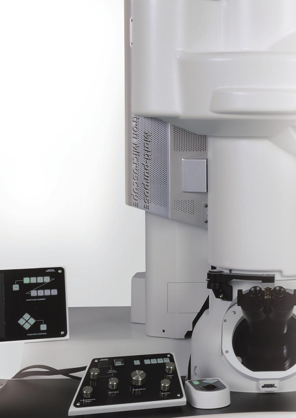
JEM-F200. Multi-purpose Electron Microscope. Scientific / Metrology Instruments Multi-purpose Electron Microscope
|
|
|
- Douglas Joseph
- 5 years ago
- Views:
Transcription


1 Scientific / Metrology Instruments Multi-purpose Electron Microscope JEM-F200 Multi-purpose Electron Microscope JEM-F200/F2 is a multi-purpose electron microscope of the new generation to meet today's diversified needs. For F2, a user-oriented integrated-control-environment has been developed without sacrificing excellent performance and while maintaining a variety of functions.
2

 and")
, are")


 2 nm")

1.3-1.4ev (d)1.5-1.")


3 Entirely revolutionized TEM F2 High-resolution analytical systems, such as transmission electron microscopes (TEM) and scanning transmission electron microscopes (STEM), are attracting increased attention. Higher resolution and higher efficiency are required for modern systems, along with upgraded ease of operation. To meet these needs, JEM-F200 (nickname: F2) has been developed as a next-generation electron microscope. High resolution STEM HAADF image STEM-HAADF image Specimen: Quasicrystal (courtesy of Professor Emeritus K. Hiraga, Tohoku University) 2 nm 10 nm -1 Surface plasmon resonance by STEM-EELS* with DeScan system* (a)haadf (b) ev (c) ev (d) ev Wide Field STEM-EELS spectra Specimen: Ag nanoparticles (courtesy of Dr. T. Sannomiya, Tokyo Institute of Technology) 500nm (e) ev (f) ev (g) ev 3D-EDS tomography* HAADF Ti Ai 3D EDS Tomograph O Si 1μm Specimen: Paint thin section * option
4 Fun to use from JEM-F200 / Multi-purpose Electron Smart design >>The operation and appearance of F2 have been built under the design concept Smart. A new user interface focusing on intuitive operation has been developed for analytical electron microscopy. By applying knowledge of mechanical and electrical stabilities accumulated over the long history of JEOL to the design of F2, the stability of the new TEM has dramatically improved. Quad-Lens condenser system >>Modern TEMs must satisfy a wide range of applications, including bright-field (BF) & dark-field (DF) TEM and STEM, as well as analysis from various types of detectors. To meet such sophisticated needs, F2 incorporates the Quad-Lens condenser system to realize independent control of electron-beam intensity and convergence angle. Advanced Scan system >>F2 is equipped with a new scanning system "Advanced Scan System", which incorporates a descan system in the imaging lens system in addition to the standard probe scanning mechanism. This achieves a wide-field energy filtered STEM. Pico Stage drive >>F2 comes with an ultra-fast, high-precision Pico stage drive, as well as a super-high-precision piezo drive mechanism. This enables the operator to move a field-of-view smoothly over a wide spatial-scale range from millimeters to picometers.

5 Microscope SPECPORTER >>F2 incorporates an automated mechanism SPECPORTER for smoother holder insertion and retraction. The mechanism allows us to insert or extract a specimen holder by simply pushing a button. Improved Cold FEG* >>F2 is equipped with an improved cold FEG (cold field emission gun) as an electron source. The narrow energy spread of the CFEG enables high-energy resolution EELS, which may identify chemical-bonding states of specimens. A high brightness and stable electron beam produced from the CFEG enables dramatically-reduced analysis time. Good temporal and spatial coherence from the CFEG provides higher quality atomic resolution images. Dual SDD* >>Two large-solid angle silicon drift detectors (SDDs) with high analytical sensitivity can be simultaneously installed into the microscope column, leading to X-ray analysis with higher sensitivity and throughput. Environmental friendly >>F2 is the first TEM to come with an ECO mode. The ECO mode system saves energy when the instrument is not used by keeping the microscope under good standby conditions. This mode suppresses energy consumption to approximately 1/5 of that compared to when the microscope is used. A scheduling function is also included in the ECO mode that allows the microscope to be recovered from ECO mode to ready-to-use states at a designated time. * option
6 Specifications Resolution *1 Point to point 0.19 nm TEM lattice image 0.10 nm STEM-HAADF image 0.14 nm Magnification *1 TEM: 20 to 2.0 M STEM: 200 to 150 M Electron gun Schottky field emission gun or Cold field emission gun Accelerating voltage *2 20 to 200 kv Max. specimen tilt angle ±80 (with Specimen High Tilting Holder) Optional accessories Energy Dispersive X-ray Spectrometer (EDS), Electron Energy Loss Spectrometer (EELS), Digital Camera * 1 When CF-UHR is configured. * 2 Standard voltages are 200 kv and 80 kv. Installation Room Requirements Room temperature 5 to 25 C (drift 1 C/h or less) Humidity 60% or less Microscope power supply Single phase 200 V, 10 kva Cooling water Flow rate: 10 L/min. Temperature: 15 to 20 C (fluctuations 0.1 C/h or less) Footprint 4,000 mm (W) 5,000 mm (D) or more Ceiling height With TFEG: 3,000 mm or more, With CFEG: 3,200 mm or more Entrance 1,000 mm (W) 2,000 mm (H) or more Height (mm) Width (mm) Depth (mm) Weight (kg) Microscope main console With TFEG 2,633 1,279 1,248 1,900 With CFEG 2,763 1,279 1,248 2,100 High-voltage tank With TFEG 1,639 1,000 1, With CFEG 1,719 1,000 1, PS console 1, Card console 1, LD console Rotary pump Air compressor * * The optional air compressor can be used only in Japan. No.1301K585C(Bn)
Introduction of New Products
 Field Emission Electron Microscope JEM-3100F For evaluation of materials in the fields of nanoscience and nanomaterials science, TEM is required to provide resolution and analytical capabilities that can
Development of JEM-2800 High Throughput Electron Microscope
 Development of JEM-2800 High Throughput Electron Microscope Mitsuhide Matsushita, Shuji Kawai, Takeshi Iwama, Katsuhiro Tanaka, Toshiko Kuba and Noriaki Endo EM Business Unit, JEOL Ltd. Electron Optics
Indiana University JEM-3200FS
 Indiana University JEM-3200FS Installation Specification Model: JEM 3200FS Serial Number: EM 15000013 Objective Lens Configuration: High Resolution Pole Piece (HRP) JEOL Engineer: Michael P. Van Etten
Transmission Electron Microscopy 9. The Instrument. Outline
 Transmission Electron Microscopy 9. The Instrument EMA 6518 Spring 2009 02/25/09 Outline The Illumination System The Objective Lens and Stage Forming Diffraction Patterns and Images Alignment and Stigmation
NanoSpective, Inc Progress Drive Suite 137 Orlando, Florida
 TEM Techniques Summary The TEM is an analytical instrument in which a thin membrane (typically < 100nm) is placed in the path of an energetic and highly coherent beam of electrons. Typical operating voltages
Appreciating the very little things: Status and future prospects of TEM at NUANCE
 Appreciating the very little things: Status and future prospects of TEM at NUANCE Dr. Roberto dos Reis roberto.reis@northwestern.edu 11/28/2018 Nature 542, pages75 79 (2017) TEM Facility Manager: Dr. Xiaobing
LVEM 25. Low Voltage Electron Microscope Fast Compact Powerful.... your way to electron microscopy
 LVEM 25 Low Voltage Electron Microscope Fast Compact Powerful... your way to electron microscopy INTRODUCING THE LVEM 25 High Contrast & High Resolution Unmatched contrast of biologic and light material
Full-screen mode Popup controls. Overview of the microscope user interface, TEM User Interface and TIA on the left and EDS on the right
 Quick Guide to Operating FEI Titan Themis G2 200 (S)TEM: TEM mode Susheng Tan Nanoscale Fabrication and Characterization Facility, University of Pittsburgh Office: M104/B01 Benedum Hall, 412-383-5978,
2014 HTD-E with options
 with options The HT7700 : a user-friendly, ergonomic digital TEM with options User-Friendly r end Design Ambient light operation. Multiple automated functions for alignment, focus and stigmation as standard
STEM alignment procedures
 STEM alignment procedures Step 1. ASID alignment mode 1. Write down STD for TEM, and then open the ASID control window from dialogue. Also, start Simple imager viewer program on the Desktop. 2. Click on
CS-TEM vs CS-STEM. FEI Titan CIME EPFL. Duncan Alexander EPFL-CIME
 CS-TEM vs CS-STEM Duncan Alexander EPFL-CIME 1 FEI Titan Themis @ CIME EPFL 60 300 kv Monochromator High brightness X-FEG Probe Cs-corrected: 0.7 Å @ 300 kv Image Cs-corrected: 0.7 Å @ 300 kv Super-X EDX
Low Voltage Electron Microscope
 LVEM5 Low Voltage Electron Microscope Nanoscale from your benchtop LVEM5 Delong America DELONG INSTRUMENTS COMPACT BUT POWERFUL The LVEM5 is designed to excel across a broad range of applications in material
Scanning electron microscope
 Scanning electron microscope 5 th CEMM workshop Maja Koblar, Sc. Eng. Physics Outline The basic principle? What is an electron? Parts of the SEM Electron gun Electromagnetic lenses Apertures Detectors
ELECTRON MICROSCOPY. 13:10 16:00, Oct. 6, 2008 Institute of Physics, Academia Sinica. Tung Hsu
 ELECTRON MICROSCOPY 13:10 16:00, Oct. 6, 2008 Institute of Physics, Academia Sinica Tung Hsu Department of Materials Science and Engineering National Tsing Hua University Hsinchu 300, TAIWAN Tel. 03-5742564
Recent results from the JEOL JEM-3000F FEGTEM in Oxford
 Recent results from the JEOL JEM-3000F FEGTEM in Oxford R.E. Dunin-Borkowski a, J. Sloan b, R.R. Meyer c, A.I. Kirkland c,d and J. L. Hutchison a a b c d Department of Materials, Parks Road, Oxford OX1
CS-TEM vs CS-STEM. FEI Titan CIME EPFL. Duncan Alexander EPFL-CIME
 CS-TEM vs CS-STEM Duncan Alexander EPFL-CIME 1 FEI Titan Themis @ CIME EPFL 60 300 kv Monochromator High brightness X-FEG Probe Cs-corrected: 0.7 Å @ 300 kv Image Cs-corrected: 0.7 Å @ 300 kv Super-X EDX
Nanotechnology in Consumer Products
 Nanotechnology in Consumer Products Advances in Transmission Electron Microscopy Friday, April 21, 2017 October 31, 2014 The webinar will begin at 1pm Eastern Time Click here to watch the webinar recording
Low Voltage Electron Microscope. Nanoscale from your benchtop LVEM5. Delong America
 LVEM5 Low Voltage Electron Microscope Nanoscale from your benchtop LVEM5 Delong America DELONG INSTRUMENTS COMPACT BUT POWERFUL The LVEM5 is designed to excel across a broad range of applications in material
Schottky Emission VP FE-SEM
 Schottky Emission VP FE-SEM Variable Pressure The Scanning Electron Microscope (SEM) has played an important role for many years for research and development of advanced materials in the leading edge of
Scanning electron microscope
 Scanning electron microscope 6 th CEMM workshop Maja Koblar, Sc. Eng. Physics Outline The basic principle? What is an electron? Parts of the SEM Electron gun Electromagnetic lenses Apertures Chamber and
Low Voltage Electron Microscope
 LVEM 25 Low Voltage Electron Microscope fast compact powerful Delong America FAST, COMPACT AND POWERFUL The LVEM 25 offers a high-contrast, high-throughput, and compact solution with nanometer resolutions.
LVEM 25. Low Voltage Electron Mictoscope. fast compact powerful
 LVEM 25 Low Voltage Electron Mictoscope fast compact powerful FAST, COMPACT AND POWERFUL The LVEM 25 offers a high-contrast, high-throughput, and compact solution with nanometer resolutions. All the benefits
The user should already be familiar with operation of the instrument in STEM mode, use of the Microscope Control interface, and TIA.
 FEI Tecnai F20 S/TEM: EDS system operation Nicholas G. Rudawski ngr@ufl.edu (805) 252-4916 (352) 392-3077 Last updated: 01/22/18 The user should already be familiar with operation of the instrument in
1.1. In regular TEM imaging mode, find a region of interest and set it at eucentric height.
 JEOL 2010F operating procedure Covers operation in STEM mode (See separate procedures for operation in TEM mode and operation of EDS system) Nicholas G. Rudawski ngr@ufl.edu (805) 252-4916 NOTE: this operating
--> Buy True-PDF --> Auto-delivered in 0~10 minutes. JY/T
 Translated English of Chinese Standard: JY/T011-1996 www.chinesestandard.net Sales@ChineseStandard.net INDUSTRY STANDARD OF THE JY PEOPLE S REPUBLIC OF CHINA General rules for transmission electron microscopy
INTRODUCTION We believe that every laboratory working in the field of nanotechnology needs an SEM, therefore we would like to introduce to you our IEM
 INTRODUCTION We believe that every laboratory working in the field of nanotechnology needs an SEM, therefore we would like to introduce to you our IEM series of SEM. In short space of time, our device
Quick and simple installation and no maintenance needed. 3 Times More affordable Than a normal SEM. Obtaining results in less than 4 minutes
 INTRODUCTION We believe that every laboratory working in the field of nanotechnology needs an SEM, therefore we would like to introduce to you our IEM series of SEM. In short space of time, our device
Magellan XHR SEM. Discover the world of extreme high resolution scanning electron microscopy
 Magellan XHR SEM Discover the world of extreme high resolution scanning electron microscopy Gold particles on carbon test sample imaged at 200 V and a horizontal field width (HFW) of 500 nm. Unprecedented
High Resolution Transmission Electron Microscopy (HRTEM) Summary 4/11/2018. Thomas LaGrange Faculty Lecturer and Senior Staff Scientist
 Summary 4/11/2018. Thomas LaGrange Faculty Lecturer and Senior Staff Scientist") Thomas LaGrange Faculty Lecturer and Senior Staff Scientist High Resolution Transmission Electron Microscopy (HRTEM) Doctoral Course MS-637 April 16-18th, 2018 Summary Contrast in TEM images results from
Thomas LaGrange Faculty Lecturer and Senior Staff Scientist High Resolution Transmission Electron Microscopy (HRTEM) Doctoral Course MS-637 April 16-18th, 2018 Summary Contrast in TEM images results from
This document assumes the user is already familiar with basic operation of the instrument in TEM mode and use of the Microscope Control interface.
 FEI Tecnai F20 S/TEM: imaging in STEM mode Nicholas G. Rudawski ngr@ufl.edu (805) 252-4916 (352) 392-3077 Last updated: 05/10/18 This document assumes the user is already familiar with basic operation
FEI Tecnai G 2 F20 Operating Procedures
 FEI Tecnai G 2 F20 Operating Procedures 1. Startup (1) Sign-up in the microscope log-sheet. Please ensure you have written an account number for billing. (2) Log in to the computer: Login to your account
STEP INTO THE WORLD OF JEOL
 Product Lineup SMART FLEXIBLE POWERFUL STEP INTO THE WORLD OF JEOL SEM TEM SAMPLE PREP NMR MASS SPEC EPMA LITHOGRAPHY Bell Lab Harvard University Osaka University JEOLUSA.COM CRYO-EM, EPMA, LITHOGRAPHY
(1) Research Institute for Scientific Measurements, Tohoku University, Katahira 2-1-1, Aoba-ku,
 Research Institute for Scientific Measurements, Tohoku University, Katahira 2-1-1, Aoba-ku,") 351 Classification Physics Abstracts 07.80 Performance of a new high-resolution electron energy-loss spectroscopy microscope Masami Thrauchi(1), Ryuichi Kuzuo(1), Futami Satoh(1), Michiyoshi Thnaka(1),
351 Classification Physics Abstracts 07.80 Performance of a new high-resolution electron energy-loss spectroscopy microscope Masami Thrauchi(1), Ryuichi Kuzuo(1), Futami Satoh(1), Michiyoshi Thnaka(1),
Introduction to Transmission Electron Microscopy (Physical Sciences)
") Introduction to Transmission Electron Microscopy (Physical Sciences) Centre for Advanced Microscopy Program 9:30 10:45 Lecture 1 Basics of TEM 10:45 11:00 Morning tea 11:00 12:15 Lecture 2 Diffraction
Introduction to Transmission Electron Microscopy (Physical Sciences) Centre for Advanced Microscopy Program 9:30 10:45 Lecture 1 Basics of TEM 10:45 11:00 Morning tea 11:00 12:15 Lecture 2 Diffraction
Introduction to Electron Microscopy
 Introduction to Electron Microscopy Prof. David Muller, dm24@cornell.edu Rm 274 Clark Hall, 255-4065 Ernst Ruska and Max Knoll built the first electron microscope in 1931 (Nobel Prize to Ruska in 1986)
M4 TORNADO PLUS. Innovation with Integrity. Super Light Element Micro-XRF Spectrometer. Micro-XRF
 M4 TORNADO PLUS Super Light Element Micro-XRF Spectrometer Innovation with Integrity Micro-XRF M4 TORNADO PLUS - A New Era in Micro-XRF M4 TORNADO PLUS is the world's first Micro-XRF spectrometer that
Chapter 2 Instrumentation for Analytical Electron Microscopy Lecture 7. Chapter 2 CHEM Fall L. Ma
 Chapter 2 Instrumentation for Analytical Electron Microscopy Lecture 7 Outline Electron Sources (Electron Guns) Thermionic: LaB 6 or W Field emission gun: cold or Schottky Lenses Focusing Aberration Probe
PERFORMANCE IN NANOSPACE PRODUCT OVERVIEW
 PERFORMANCE IN NANOSPACE PRODUCT OVERVIEW TESCAN Brno, s.r.o. was established as subsidiary of a multi-national company TESCAN ORSAY HOLDING after the merger (August 2013) of Czech company TESCAN, a global
Transmissions Electron Microscopy (TEM)
") Transmissions Electron Microscopy (TEM) Basic principles Diffraction Imaging Specimen preparation A.E. Gunnæs MENA3100 V17 TEM is based on three possible set of techniqes Diffraction From regions down
Transmissions Electron Microscopy (TEM) Basic principles Diffraction Imaging Specimen preparation A.E. Gunnæs MENA3100 V17 TEM is based on three possible set of techniqes Diffraction From regions down
ELECTRON MICROSCOPY. 14:10 17:00, Apr. 3, 2007 Department of Physics, National Taiwan University. Tung Hsu
 ELECTRON MICROSCOPY 14:10 17:00, Apr. 3, 2007 Department of Physics, National Taiwan University Tung Hsu Department of Materials Science and Engineering National Tsinghua University Hsinchu 300, TAIWAN
Basic Users Manual for Tecnai-F20 TEM
 Basic Users Manual for Tecnai-F20 TEM NB: This document contains my personal notes on the operating procedure of the Tecnai F20 and may be used as a rough guide for those new to the microscope. It may
1.2. Make sure the viewing screen is covered (exposure to liquid N 2 may cause it to crack).
.") FEI Tecnai F20 S/TEM: imaging in TEM mode Nicholas G. Rudawski ngr@ufl.edu (805) 252-4916 (352) 392-3077 Last updated: 01/21/18 1. Filling the cold trap (if needed) 1.1. Prior to use, the cold trap needs
FEI Tecnai F20 S/TEM: imaging in TEM mode Nicholas G. Rudawski ngr@ufl.edu (805) 252-4916 (352) 392-3077 Last updated: 01/21/18 1. Filling the cold trap (if needed) 1.1. Prior to use, the cold trap needs
ELECTRON MICROSCOPY. 09:10 12:00, Oct. 27, 2006 Institute of Physics, Academia Sinica. Tung Hsu
 ELECTRON MICROSCOPY 09:10 12:00, Oct. 27, 2006 Institute of Physics, Academia Sinica Tung Hsu Department of Materials Science and Engineering National Tsinghua University Hsinchu 300, TAIWAN Tel. 03-5742564
Introduction: Why electrons?
 Introduction: Why electrons? 1 Radiations Visible light X-rays Electrons Neutrons Advantages Not very damaging Easily focused Eye wonderful detector Small wavelength (Angstroms) Good penetration Small
SCIENTIFIC INSTRUMENT NEWS. Introduction. Design of the FlexSEM 1000
 SCIENTIFIC INSTRUMENT NEWS 2017 Vol. 9 SEPTEMBER Technical magazine of Electron Microscope and Analytical Instruments. Technical Explanation The FlexSEM 1000: A Scanning Electron Microscope Specializing
Functions of the SEM subsystems
 Functions of the SEM subsystems Electronic column It consists of an electron gun and two or more electron lenses, which influence the path of electrons traveling down an evacuated tube. The base of the
STEM Spectrum Imaging Tutorial
 STEM Spectrum Imaging Tutorial Gatan, Inc. 5933 Coronado Lane, Pleasanton, CA 94588 Tel: (925) 463-0200 Fax: (925) 463-0204 April 2001 Contents 1 Introduction 1.1 What is Spectrum Imaging? 2 Hardware 3
Low-energy Electron Diffractive Imaging for Three dimensional Light-element Materials
 Low-energy Electron Diffractive Imaging for Three dimensional Light-element Materials Hitachi Review Vol. 61 (2012), No. 6 269 Osamu Kamimura, Ph. D. Takashi Dobashi OVERVIEW: Hitachi has been developing
Fast Laser Raman Microscope RAMAN
 Fast Laser Raman Microscope RAMAN - 11 www.nanophoton.jp Fast Raman Imaging A New Generation of Raman Microscope RAMAN-11 developed by Nanophoton was created by combining confocal laser microscope technology
Titan on-line help manual -- Working with a FEG
 1 manual -- Working with a FEG Table of Contents 1 FEG Safety... 2 1.1 The column valves... 2 2 FEG States... 2 3 Starting the FEG... 4 4 Shutting the FEG down... 6 5 FEG Design... 6 5.1 Electron source...
Leading in Desktop SEM Imaging and Analysis
 Leading in Desktop SEM Imaging and Analysis Fast. Outstanding. Reliable SEM imaging and analysis. The Phenom: World s Fastest Scanning Electron Microscope With its market-leading Phenom desktop Scanning
Philip Sperling. Sales Science and New Materials, YXLON International GmbH, Essener Bogen 15, Hamburg, Germany.
 A new generation of x-ray computed tomography devices for quality inspection and metrology inspection in the field of additive manufacturing and other sciences Philip Sperling Sales Science and New Materials,
PERFORMANCE IN NANOSPACE PRODUCT OVERVIEW
 PERFORMANCE IN NANOSPACE PRODUCT OVERVIEW TESCAN, a.s. is a Czech joint-stock company focused on research, development and manufacture of scientific instruments and laboratory equipment such as: scanning
Fast Laser Raman Microscope RAMAN
 Fast Laser Raman Microscope RAMAN - 11 www.nanophoton.jp Fast Raman Imaging A New Generation of Raman Microscope RAMAN-11 developed by Nanophoton was created by combining confocal laser microscope technology
MSE 460 TEM Lab 2: Basic Alignment and Operation of Microscope
 MSE 460 TEM Lab 2: Basic Alignment and Operation of Microscope Last updated on 1/8/2018 Jinsong Wu, jinsong-wu@northwestern.edu Aims: The aim of this lab is to familiarize you with basic TEM alignment
FEI Falcon Direct Electron Detector. Best Practice Document
 FEI Falcon Direct Electron Detector Best Practice Document 2 1. Introduction FEI Falcon Direct Electron Detector Best Practice Application Guide The FEI Falcon Detector is based on direct electron detection
SCANNING ELECTRON MICROSCOPY AND X-RAY MICROANALYSIS
 SCANNING ELECTRON MICROSCOPY AND X-RAY MICROANALYSIS Robert Edward Lee Electron Microscopy Center Department of Anatomy and Neurobiology Colorado State University P T R Prentice Hall, Englewood Cliffs,
Introduction to Electron Microscopy-II
 Introduction to Electron Microscopy-II Prof. David Muller, dm24@cornell.edu Rm 274 Clark Hall, 255-4065 Ernst Ruska and Max Knoll built the first electron microscope in 1931 (Nobel Prize to Ruska in 1986)
University of Washington Molecular Analysis Facility
 University of Washington Molecular Analysis Facility Apreo-S (Variable Pressure) is a Schottky Field Emission Scanning Electron Microscope (FESEM) that combines high- and low-voltage ultra-high resolution
Electron Sources, Optics and Detectors
 Thomas LaGrange, Ph.D. Faculty Lecturer and Senior Staff Scientist Electron Sources, Optics and Detectors TEM Doctoral Course MS-637 April 16 th -18 th, 2018 Summary Electron propagation is only possible
LEO 912 TEM Short Manual. Prepared/copyrighted by RH Berg Danforth Plant Science Center
 LEO 912 TEM Short Manual Prepared/copyrighted by RH Berg Danforth Plant Science Center Specimen holder [1] Never touch the holder (outside of the O-ring, double-headed arrow) because finger oils will contaminate
MSE 595T Transmission Electron Microscopy. Laboratory III TEM Imaging - I
 MSE 595T Basic Transmission Electron Microscopy TEM Imaging - I Purpose The purpose of this lab is to: 1. Make fine adjustments to the microscope alignment 2. Obtain a diffraction pattern 3. Obtain an
2. Raise HT to 200kVby following the procedure explained in 1.6.
 JEOL 2100 MANUAL Quick check list 1. If needed, fill the reservoir with LN2 2. Raise HT to 200kVby following the procedure explained in 1.6. 3. Insert specimen holder into TEM (Insert holder in airlock,
Standard Operating Procedure for the Amray 1810 Scanning Electron Microscope Version: 29 NOVEMBER 2014
 Standard Operating Procedure for the Amray 1810 Scanning Electron Microscope Version: 29 NOVEMBER 2014 1. Utility Requirements a. System power is supplied by two 120 VAC/20 A circuits. When doing maintenance
1.3. Before loading the holder into the TEM, make sure the X tilt is set to zero and the goniometer locked in place (this will make loading easier).
.") JEOL 200CX operating procedure Nicholas G. Rudawski ngr@ufl.edu (805) 252-4916 1. Specimen loading 1.1. Unlock the TUMI system. 1.2. Load specimen(s) into the holder. If using the double tilt holder, ensure
JEOL 200CX operating procedure Nicholas G. Rudawski ngr@ufl.edu (805) 252-4916 1. Specimen loading 1.1. Unlock the TUMI system. 1.2. Load specimen(s) into the holder. If using the double tilt holder, ensure
Advanced Materials Characterization Workshop
 University of Illinois at Urbana-Champaign Materials Research Laboratory Advanced Materials Characterization Workshop June 3 rd and 4 th, 2013 Transmission Electron Microscopy Wacek Swiech, Honghui Zhou,
NANO 703-Notes. Chapter 9-The Instrument
 1 Chapter 9-The Instrument Illumination (condenser) system Before (above) the sample, the purpose of electron lenses is to form the beam/probe that will illuminate the sample. Our electron source is macroscopic
Spotlight 150 and 200 FT-IR Microscopy Systems
 S P E C I F I C A T I O N S Spotlight 150 and 200 FT-IR Microscopy Systems FT-IR Microscopy Spotlight 200 with Frontier FT-IR Spectrometer Introduction PerkinElmer Spotlight FT-IR Microscopy Systems are
INSTRUCTIONS JEM-2010F FIELD-EMISSION TRANSMISSION ELECTRON MICROSCOPE WITH STEM CAPABILITY
 INSTRUCTIONS JEM-2010F FIELD-EMISSION TRANSMISSION ELECTRON MICROSCOPE WITH STEM CAPABILITY August 2011 PRELIMINARIES OPERATION 1. Ensure that EMISSION and HT are on: The HT READY and FEG READY lights
Chapter 4 Imaging Lecture 17
 Chapter 4 Imaging Lecture 17 d (110) Imaging Imaging in the TEM Diffraction Contrast in TEM Image HRTEM (High Resolution Transmission Electron Microscopy) Imaging STEM imaging Imaging in the TEM What is
ELECTRON MICROSCOPY AN OVERVIEW
 ELECTRON MICROSCOPY AN OVERVIEW Anjali Priya 1, Abhishek Singh 2, Nikhil Anand Srivastava 3 1,2,3 Department of Electrical & Instrumentation, Sant Longowal Institute of Engg. & Technology, Sangrur, India.
2.Components of an electron microscope. a) vacuum systems, b) electron guns, c) electron optics, d) detectors. Marco Cantoni 021/
 vacuum systems, b) electron guns, c) electron optics, d) detectors. Marco Cantoni 021/") 2.Components of an electron microscope a) vacuum systems, b) electron guns, c) electron optics, d) detectors, 021/693.48.16 Centre Interdisciplinaire de Microscopie Electronique CIME Summary Electron propagation
2.Components of an electron microscope a) vacuum systems, b) electron guns, c) electron optics, d) detectors, 021/693.48.16 Centre Interdisciplinaire de Microscopie Electronique CIME Summary Electron propagation
S200 Course LECTURE 1 TEM
 S200 Course LECTURE 1 TEM Development of Electron Microscopy 1897 Discovery of the electron (J.J. Thompson) 1924 Particle and wave theory (L. de Broglie) 1926 Electromagnetic Lens (H. Busch) 1932 Construction
Scanning Electron Microscopy. EMSE-515 F. Ernst
 Scanning Electron Microscopy EMSE-515 F. Ernst 1 2 Scanning Electron Microscopy Max Knoll Manfred von Ardenne Manfred von Ardenne Principle of Scanning Electron Microscopy 3 Principle of Scanning Electron
Procedures for Performing Cryoelectron Microscopy on the FEI Sphera Microscope
 Procedures for Performing Cryoelectron Microscopy on the FEI Sphera Microscope The procedures given below were written specifically for the FEI Tecnai G 2 Sphera microscope. Modifications will need to
The application of spherical aberration correction and focal series restoration to high-resolution images of platinum nanocatalyst particles
 Journal of Physics: Conference Series The application of spherical aberration correction and focal series restoration to high-resolution images of platinum nanocatalyst particles Recent citations - Miguel
OPERATION OF THE HITACHI S-450 SCANNING ELECTRON MICROSCOPE. by Doug Bray Department of Biological Sciences University of Lethbridge
 OPERATION OF THE HITACHI S-450 SCANNING ELECTRON MICROSCOPE by Doug Bray Department of Biological Sciences University of Lethbridge Revised September, 2000 Note: The terms in bold in this document represent
Operating Checklist for using the Scanning Electron. Microscope, JEOL JSM 6400.
 Smith College August 2009 Operating Checklist for using the Scanning Electron Microscope, JEOL JSM 6400. CONTENT, page no. Pre-Check 1 Startup 1 Specimen Insertion 2 Filament Saturation 2 Beam Alignment
Measurement of Surface Profile and Layer Cross-section with Wide Field of View and High Precision
 Hitachi Review Vol. 65 (2016), No. 7 243 Featured Articles Measurement of Surface Profile and Layer Cross-section with Wide Field of View and High Precision VS1000 Series Coherence Scanning Interferometer
How to choose a Scanning Electron Microscope (SEM)
") www.lambdaphoto.co.uk E-guide How to choose a Scanning Electron Microscope (SEM) Providing guidance in the selection of the right microscope for your research Distribution in the UK & Ireland Table of
www.lambdaphoto.co.uk E-guide How to choose a Scanning Electron Microscope (SEM) Providing guidance in the selection of the right microscope for your research Distribution in the UK & Ireland Table of
Fastest high definition Raman imaging. Fastest Laser Raman Microscope RAMAN
 Fastest high definition Raman imaging Fastest Laser Raman Microscope RAMAN - 11 www.nanophoton.jp Observation A New Generation in Raman Observation RAMAN-11 developed by Nanophoton was newly created by
Operating Checklist for using the Scanning Electron Microscope, JEOL JSM 6400.
 Smith College August 2005 Operating Checklist for using the Scanning Electron Microscope, JEOL JSM 6400. CONTENT, page no. Pre-Check, 1 Specimen Insertion, 1 Startup, 2 Filament Saturation, 2 Beam Alignment,
Please follow these instructions for use of the Philips CM100 TEM. Adopted from website below.
 Please follow these instructions for use of the Philips CM100 TEM. Adopted from website below. http://staff.washington.edu/wpchan/if/cm100_inst.shtml Instructions for the Philips CM100 TEM and peripherals
Introduction to Scanning Electron Microscopy
 Introduction to Scanning Electron Microscopy By: Brandon Cheney Ant s Leg Integrated Circuit Nano-composite This document was created as part of a Senior Project in the Materials Engineering Department
Manufacturing Metrology Team
 The Team has a range of state-of-the-art equipment for the measurement of surface texture and form. We are happy to discuss potential measurement issues and collaborative research Manufacturing Metrology
v tome x m microfocus CT
 GE Inspection Technologies v tome x m microfocus CT Uniting premium 3D metrology and inspection with quality and speed. gemeasurement.com/ct x plore precision CT line Inspect with precision, power, and
MODULE I SCANNING ELECTRON MICROSCOPE (SEM)
") MODULE I SCANNING ELECTRON MICROSCOPE (SEM) Scanning Electron Microscope (SEM) Initially, the plan of SEM was offered by H. Stintzing in 1927 (a German patent application). His suggested procedure was
MODULE I SCANNING ELECTRON MICROSCOPE (SEM) Scanning Electron Microscope (SEM) Initially, the plan of SEM was offered by H. Stintzing in 1927 (a German patent application). His suggested procedure was
Cryo-Electron Microscopy of Viruses
 Blockkurs Biophysic and Structural Biology 2013 Praktikumsversuch at C-CINA Cryo-Electron Microscopy of Viruses In this practical we will compare electron microscopy of negatively stained and frozen-hydrated
Huvitz Digital Microscope HDS-5800
 Huvitz Digital Microscope HDS-5800 Dimensions unit : mm Huvitz Digital Microscope HDS-5800 HDS-MC HDS-SS50 The world s first, convert the magnification from 50x to 5,800x with a zoom lens HDS-TS50 Huvitz
General information. If you see the instrument turned off, notify MIC personnel. MIC personnel will help you insert your samples into the instrument.
 JEOL JSM-7400F Table of contents General information.. 3 The operation panel. 4 The different sample holders and inserting the samples.. 5 Turning on the beam... 6 Stage map control... 8 Correcting astigmatism...
TEM theory Basic optics, image formation and key elements
 Workshop series of Chinese 3DEM community Get acquainted with Cryo-Electron Microscopy: First Chinese Workshop for Structural Biologists TEM theory Basic optics, image formation and key elements Jianlin
JEOL 2010 FasTEM & DigitalMicrograph User's Guide
 JEOL 2010 FasTEM & DigitalMicrograph User's Guide Electron Microscopy Laboratory Instititute of Materials Science University of Connecticut The purpose of this manual is to remind you of the essential
Basic Operating Instructions for Strata Dual Beam 235 FIB/SEM
 Basic Operating Instructions for Strata Dual Beam 235 FIB/SEM Warning Always adjust your specimen height before closing the chamber door to make sure your specimen will not hit the bottom of the lens;
Instructions for Tecnai a brief start up manual
 Instructions for Tecnai a brief start up manual Version 3.0, 8.12.2015 Manual of Tecnai 12 transmission electron microscope located at Aalto University's Nanomicroscopy Center. More information of Nanomicroscopy
Scanning Electron Microscopy SEM. Warren Straszheim, PhD MARL, 23 Town Engineering
 Scanning Electron Microscopy SEM Warren Straszheim, PhD MARL, 23 Town Engineering wesaia@iastate.edu 515-294-8187 How it works Create a focused electron beam Accelerate it Scan it across the sample Map
Evaluating the Performance of a Commercial Silicon Drift Detector for X-ray Microanalysis
 Evaluating the Performance of a Commercial Silicon Drift Detector for X-ray Microanalysis Edward A. Kenik Materials Science & Technology Division, Oak Ridge National Laboratory, Oak Ridge, TN 37831 kenikea@ornl.gov
Scanning Electron Microscopy Basics and Applications
 Scanning Electron Microscopy Basics and Applications Dr. Julia Deuschle Stuttgart Center for Electron Microscopy MPI for Solid State Research Room: 1E15, phone: 0711/ 689-1193 email: j.deuschle@fkf.mpg.de
High-resolution imaging on C s -corrected Titan
 High-resolution imaging on C s -corrected Titan 80-300 A new era for new results In NanoResearch a detailed knowledge of the structure of the material down to the atomic level is crucial for understanding
picoemerald Tunable Two-Color ps Light Source Microscopy & Spectroscopy CARS SRS
 picoemerald Tunable Two-Color ps Light Source Microscopy & Spectroscopy CARS SRS 1 picoemerald Two Colors in One Box Microscopy and Spectroscopy with a Tunable Two-Color Source CARS and SRS microscopy