Nanotechnology in Consumer Products
|
|
|
- Hester Horn
- 5 years ago
- Views:
Transcription


1 Nanotechnology in Consumer Products Advances in Transmission Electron Microscopy Friday, April 21, 2017 October 31, 2014 The webinar will begin at 1pm Eastern Time Click here to watch the webinar recording
2 Advances in transmission electron microscopy Tom Sharp LeRoy-Eyring Center for Solid State Science Arizona State University
3 Improving microscope resolution DA Muller (2009) Nature Materials Resolution of an optical microscope is limited by the diffraction limit: δ = 0.6λ/nsinα Resolution could be improved by reducing the wavelength (λ) δ = 0.6λ/nsinα

4 The first electron microscope Ruska and Knoll in the 1931.
")
5 John Cowley with Sumio Iijima John Cowley with Sumio Iijima at the controls of the JEM-100B (Tempe, 1974)

6 Layout of a Transmission Electron Microscope

7 Electron Matter Interactions Electrons are easily scattered. Elastic scattering no change in energy. diffraction Inelastic scattering transferring energy to the sample. Used for microanalysis:


8 Electron imaging and diffraction Back focal Back focal plane diffraction pattern Image plane - image Kaolinite along [001]
9 Diffraction Contrast Imaging Each diffracted spot corresponds to a set of lattice planes. Each spot contains information from the entire image (selected) Bright-Field Imaging Use only the central spot. Dark-Field Imaging Use one of the diffracted spots Tilt the crystal to or near a Bragg condition
![DF Image of Olivine dislocations, b=[100] Complex mixed](/docs-images/95/123877631/images/10-0.jpg "character Edge and screw dislocations in a (010) foil")
 Tilt boundaries along (100) Edge](/docs-images/95/123877631/images/10-2.jpg "dislocations with u ~ [010] Slip system [100](001) g =")
10 DF Image of Olivine dislocations, b=[100] Complex mixed character Edge and screw dislocations in a (010) foil Slip system [100](010) Tilt boundaries along (100) Edge dislocations with u ~ [010] Slip system [100](001) g = 400
11 HRTEM (Phase Contrast) Imaging down a zone axis many diffracted beams. Use a large objective aperture. Image of the crystal lattice with nearly atomic resolution Phase contrast Contrast from phase differences between the diffracted beams. Dynamic diffraction Complex image contrast variations with sample thickness and defocus.

12 Zircon twin boundary Phase contrast image alon [111] showing damaged regions that appear lighter.

13 Zircon twin boundary (11-2) Higher magnification image of disordered domains.
14 Improving TEM resolution DA Muller (2009) Nature Materials For electron microscope the (Scherzer) resolution is given by δ = 0.66λ 3/4 C s 1/4 Increase the accelerating voltage to reduce the wavelength. δ = 0.6λ/nsinα

15 Historical approach to resolution improvement Use higher-voltages for shorter wavelengths Problems: Difficult to house a giant TEM Electron beam damage Hitachi 1-MeV FE-HRTEM Tonomura, J. Electron Micr. 52, 11 (2003)


16 World record lattice fringe spacing Lattice fringes at 1.0 MeV - beyond 0.5Å from Kawasaki et al., Appl. Phys. Lett. 76, 1342 (2000)
17 Improving TEM resolution DA Muller (2009) Nature Materials For electron microscope the (Scherzer) resolution is given by δ = 0.66λ 3/4 C s 1/4 Modern microscopes correct the C s δ = 0.6λ/nsinα Aberration corrected TEM and STEM
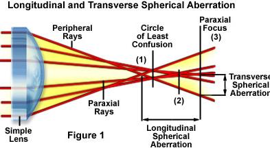
18 Spherical Aberration


19 Aberration-correction in TEM Design of the first successful aberration-corrected 200-keV FEG-TEM GaAs showing individual atomic columns after application of Cs correction. Atoms separated by 1.4 Å Schematic drawing of aberration correction device placed between objective and diffraction lenses. from Haider, et al., Ultramicroscopy, 75, 53 (1998)

20 Aberration-correction in STEM C s -corrected Non-corrected C c -effect Allowing use of large objective aperture Smaller probe size Higher probe current 100 KV (Krivanek)


21 Southwest Center for Aberration Corrected Electron Microscopy Building designed to meet environmental needs of aberration-corrected STEM/TEM 4-foot thick Isolated foundation for vibration isolation Isolated power with no ground loops in floor or walls Tight temperature control with minimal airflow Space for four advanced microscopes:

22 Jeol ARM200F Aberration-Corrected STEM for Imaging and Spectrum Mapping Operates at 80, 120, and 200 kv. Field-emission electron gun Corrector: CEOS CESCOR STEM 200 kv ~ 80 kv ~ 1.2 Å JEOL EDX Detector (0.24 ster) Gatan Enfinium EELS spectrometer Aberration Corrector
 Low-angle ADF (LAADF) Medium-angle ADF (MAADF) High-angle")
23 Formation of STEM images Bright-field STEM Annular bright-field (ABF) Large-angle BF (LABF) Low-angle ADF (LAADF) Medium-angle ADF (MAADF) High-angle ADF (HAADF)


24 STEM Imaging ABF BF: Bright-field; DF: Dark-field ABF: annular-bright-field MAADF: medium-angle annular-df HAADF: high-angle annular-df Courtesy of Lin Zhou Simultaneous HAADF and BF images of endotaxially anchored PdZn alloy nanoparticle on ZnO nanowire. Courtesy of Jingyue Liu Annular-bright-field image and line scan showing onemonolayer-thick InN quantum wells in GaN matrix.

25 Imaging of a LaMnO3/SrTiO3 interface Fast collection of EELS spectra combined with STEM imaging Atomic-resolution chemical mapping LaMnO3 SrTiO3 STEM HAADF image of SrTiO3/LaMnO3 interface, used as survey image for EELS Spectrum imaging

26 EELS Spectrum Imaging Chemical mapping across LaMnO 3 /SrTiO 3 interface. Courtesy of Paolo Longo

27 NION UltraSTEM Monochromated STEM/EELS at 40/60/100kV Nion high-energy resolution monochromated EELS systems (HERMES) Typical on ASU mev 15 mev Small zero-loss tails ASU record 12 mev O.L. Krivanek et al. Microcopy 62(1) 3-21 (2013).


28 X Y X Y From Krivanek, et al. Nature, 29 March, 2010

29

30 Aloof beam spectroscopy of radiation sensitive materials HAADF Transmission mode States in the band gap Band gap Aloof mode Band gap C-K N-K VEELS of C 3 N 4 in transmission and aloof modes. Diane Haiber et al M&M 2016 HAADF images of C3N4 and EELS spectrum showing C-K and N-K edges

 @ 80 kv ~ 1 Å (mono on) Analytical (S)TEM: EDAX EDX Detector (0.")
31 FEI Titan ETEM (S)TEM that operates at 80, 200, & 300 kv. X-FEG: Ultrahigh-brightness electron gun Monochromator: Energy resolution ~ 0.15 ev Imaging Corrector: CEOS CETCOR Information 300 kv < kv ~ 1.9 Å (mono 80 kv ~ 1 Å (mono on) Analytical (S)TEM: EDAX EDX Detector (0.13sr) Gatan Imaging Filter/EELS spectrometer Negative C S imaging of γ-al 2 O 3 / SrTiO 3 heterostructure imaged down the [110] zone axis. The oxygen and metal atomic columns are well-resolved and appear as white spots.


32 Detonation nanodiamond particles < 3 nm imaged at 80kV using monochromator. Reconstructed surfaces and twins are visible at the atomic level. Low Voltage Imaging

33 Environmental TEM Environmental TEM: Samples to be exposed to gaseous environment. TEM allows rapid imaging and movies with atomic resolution. In-house gas system allows precise control and accurate mixing. Heating and Cooling Holders: Sample observation at temperatures up to 1100 C or down to -170 C.


34 FEI Titan Krios FEI Titan Krios with a Gatan K2 Summit single-electron detector 2-3Å resolution in biological macromolecules Single particle analysis of proteins Cryo-electron tomography of cell structures

35 Nikolaus Grigorieff, ASU Cryo-EM Winter School

36

37 Webinar Recordings & Slides To access this recording and slides Or
38 Thank You! Thank you for attending the NACK Network & NCI-SW webinar Please take a moment to complete our survey
CS-TEM vs CS-STEM. FEI Titan CIME EPFL. Duncan Alexander EPFL-CIME
 CS-TEM vs CS-STEM Duncan Alexander EPFL-CIME 1 FEI Titan Themis @ CIME EPFL 60 300 kv Monochromator High brightness X-FEG Probe Cs-corrected: 0.7 Å @ 300 kv Image Cs-corrected: 0.7 Å @ 300 kv Super-X EDX
CS-TEM vs CS-STEM. FEI Titan CIME EPFL. Duncan Alexander EPFL-CIME
 CS-TEM vs CS-STEM Duncan Alexander EPFL-CIME 1 FEI Titan Themis @ CIME EPFL 60 300 kv Monochromator High brightness X-FEG Probe Cs-corrected: 0.7 Å @ 300 kv Image Cs-corrected: 0.7 Å @ 300 kv Super-X EDX
NanoSpective, Inc Progress Drive Suite 137 Orlando, Florida
 TEM Techniques Summary The TEM is an analytical instrument in which a thin membrane (typically < 100nm) is placed in the path of an energetic and highly coherent beam of electrons. Typical operating voltages
Appreciating the very little things: Status and future prospects of TEM at NUANCE
 Appreciating the very little things: Status and future prospects of TEM at NUANCE Dr. Roberto dos Reis roberto.reis@northwestern.edu 11/28/2018 Nature 542, pages75 79 (2017) TEM Facility Manager: Dr. Xiaobing
Introduction to Transmission Electron Microscopy (Physical Sciences)
") Introduction to Transmission Electron Microscopy (Physical Sciences) Centre for Advanced Microscopy Program 9:30 10:45 Lecture 1 Basics of TEM 10:45 11:00 Morning tea 11:00 12:15 Lecture 2 Diffraction
Introduction to Transmission Electron Microscopy (Physical Sciences) Centre for Advanced Microscopy Program 9:30 10:45 Lecture 1 Basics of TEM 10:45 11:00 Morning tea 11:00 12:15 Lecture 2 Diffraction
Indiana University JEM-3200FS
 Indiana University JEM-3200FS Installation Specification Model: JEM 3200FS Serial Number: EM 15000013 Objective Lens Configuration: High Resolution Pole Piece (HRP) JEOL Engineer: Michael P. Van Etten
Introduction to Electron Microscopy
 Introduction to Electron Microscopy Prof. David Muller, dm24@cornell.edu Rm 274 Clark Hall, 255-4065 Ernst Ruska and Max Knoll built the first electron microscope in 1931 (Nobel Prize to Ruska in 1986)
Introduction of New Products
 Field Emission Electron Microscope JEM-3100F For evaluation of materials in the fields of nanoscience and nanomaterials science, TEM is required to provide resolution and analytical capabilities that can
Electron
 Electron 1897: Sir Joseph John Thomson (1856-1940) discovered corpuscles small particles with a charge-to-mass ratio over 1000 times greater than that of protons. Plum pudding model : electrons in a sea
Advanced Materials Characterization Workshop
 University of Illinois at Urbana-Champaign Materials Research Laboratory Advanced Materials Characterization Workshop June 3 rd and 4 th, 2013 Transmission Electron Microscopy Wacek Swiech, Honghui Zhou,
Chapter 2 Instrumentation for Analytical Electron Microscopy Lecture 7. Chapter 2 CHEM Fall L. Ma
 Chapter 2 Instrumentation for Analytical Electron Microscopy Lecture 7 Outline Electron Sources (Electron Guns) Thermionic: LaB 6 or W Field emission gun: cold or Schottky Lenses Focusing Aberration Probe
Atomic-Level Control of the Thermoelectric Properties in Polytypoid Nanowires
 Atomic-Level Control of the Thermoelectric Properties in Polytypoid Nanowires Sean C. Andrews 1,2 *, Melissa A. Fardy 1,2 *, Michael C. Moore 1,2 *, Shaul Aloni 2, Minjuan Zhang 3, Velimir Radmilovic 2,4,
JEM-F200. Multi-purpose Electron Microscope. Scientific / Metrology Instruments Multi-purpose Electron Microscope
 Scientific / Metrology Instruments Multi-purpose Electron Microscope JEM-F200 Multi-purpose Electron Microscope JEM-F200/F2 is a multi-purpose electron microscope of the new generation to meet today's
STEM alignment procedures
 STEM alignment procedures Step 1. ASID alignment mode 1. Write down STD for TEM, and then open the ASID control window from dialogue. Also, start Simple imager viewer program on the Desktop. 2. Click on
Chapter 1. Basic Electron Optics (Lecture 2)
") Chapter 1. Basic Electron Optics (Lecture 2) Basic concepts of microscope (Cont ) Fundamental properties of electrons Electron Scattering Instrumentation Basic conceptions of microscope (Cont ) Ray diagram
Chapter 1. Basic Electron Optics (Lecture 2) Basic concepts of microscope (Cont ) Fundamental properties of electrons Electron Scattering Instrumentation Basic conceptions of microscope (Cont ) Ray diagram
A Tutorial on Electron Microscopy
 A Tutorial on Electron Microscopy Jian-Min (Jim) Zuo Mat. Sci. Eng. and Seitz-Materials Research Lab., UIUC Outline of This Tutorial I. Science and opportunities of electron microscopy II. The basic TEM,
High Resolution Transmission Electron Microscopy (HRTEM) Summary 4/11/2018. Thomas LaGrange Faculty Lecturer and Senior Staff Scientist
 Summary 4/11/2018. Thomas LaGrange Faculty Lecturer and Senior Staff Scientist") Thomas LaGrange Faculty Lecturer and Senior Staff Scientist High Resolution Transmission Electron Microscopy (HRTEM) Doctoral Course MS-637 April 16-18th, 2018 Summary Contrast in TEM images results from
Thomas LaGrange Faculty Lecturer and Senior Staff Scientist High Resolution Transmission Electron Microscopy (HRTEM) Doctoral Course MS-637 April 16-18th, 2018 Summary Contrast in TEM images results from
Chapter 4 Imaging Lecture 17
 Chapter 4 Imaging Lecture 17 d (110) Imaging Imaging in the TEM Diffraction Contrast in TEM Image HRTEM (High Resolution Transmission Electron Microscopy) Imaging STEM imaging Imaging in the TEM What is
Introduction to Electron Microscopy-II
 Introduction to Electron Microscopy-II Prof. David Muller, dm24@cornell.edu Rm 274 Clark Hall, 255-4065 Ernst Ruska and Max Knoll built the first electron microscope in 1931 (Nobel Prize to Ruska in 1986)
ELECTRON MICROSCOPY. 13:10 16:00, Oct. 6, 2008 Institute of Physics, Academia Sinica. Tung Hsu
 ELECTRON MICROSCOPY 13:10 16:00, Oct. 6, 2008 Institute of Physics, Academia Sinica Tung Hsu Department of Materials Science and Engineering National Tsing Hua University Hsinchu 300, TAIWAN Tel. 03-5742564
The application of spherical aberration correction and focal series restoration to high-resolution images of platinum nanocatalyst particles
 Journal of Physics: Conference Series The application of spherical aberration correction and focal series restoration to high-resolution images of platinum nanocatalyst particles Recent citations - Miguel
Recent results from the JEOL JEM-3000F FEGTEM in Oxford
 Recent results from the JEOL JEM-3000F FEGTEM in Oxford R.E. Dunin-Borkowski a, J. Sloan b, R.R. Meyer c, A.I. Kirkland c,d and J. L. Hutchison a a b c d Department of Materials, Parks Road, Oxford OX1
Full-screen mode Popup controls. Overview of the microscope user interface, TEM User Interface and TIA on the left and EDS on the right
 Quick Guide to Operating FEI Titan Themis G2 200 (S)TEM: TEM mode Susheng Tan Nanoscale Fabrication and Characterization Facility, University of Pittsburgh Office: M104/B01 Benedum Hall, 412-383-5978,
NANO 703-Notes. Chapter 9-The Instrument
 1 Chapter 9-The Instrument Illumination (condenser) system Before (above) the sample, the purpose of electron lenses is to form the beam/probe that will illuminate the sample. Our electron source is macroscopic
Low-energy Electron Diffractive Imaging for Three dimensional Light-element Materials
 Low-energy Electron Diffractive Imaging for Three dimensional Light-element Materials Hitachi Review Vol. 61 (2012), No. 6 269 Osamu Kamimura, Ph. D. Takashi Dobashi OVERVIEW: Hitachi has been developing
Development of JEM-2800 High Throughput Electron Microscope
 Development of JEM-2800 High Throughput Electron Microscope Mitsuhide Matsushita, Shuji Kawai, Takeshi Iwama, Katsuhiro Tanaka, Toshiko Kuba and Noriaki Endo EM Business Unit, JEOL Ltd. Electron Optics
2014 HTD-E with options
 with options The HT7700 : a user-friendly, ergonomic digital TEM with options User-Friendly r end Design Ambient light operation. Multiple automated functions for alignment, focus and stigmation as standard
ELECTRON MICROSCOPY. 14:10 17:00, Apr. 3, 2007 Department of Physics, National Taiwan University. Tung Hsu
 ELECTRON MICROSCOPY 14:10 17:00, Apr. 3, 2007 Department of Physics, National Taiwan University Tung Hsu Department of Materials Science and Engineering National Tsinghua University Hsinchu 300, TAIWAN
TEM theory Basic optics, image formation and key elements
 Workshop series of Chinese 3DEM community Get acquainted with Cryo-Electron Microscopy: First Chinese Workshop for Structural Biologists TEM theory Basic optics, image formation and key elements Jianlin
Nanotechnology and material science Lecture V
 Most widely used nanoscale microscopy. Based on possibility to create bright electron beam with sub-nm spot size. History: Ernst Ruska (1931), Nobel Prize (1986) For visible light λ=400-700nm, for electrons
ELECTRON MICROSCOPY. 09:10 12:00, Oct. 27, 2006 Institute of Physics, Academia Sinica. Tung Hsu
 ELECTRON MICROSCOPY 09:10 12:00, Oct. 27, 2006 Institute of Physics, Academia Sinica Tung Hsu Department of Materials Science and Engineering National Tsinghua University Hsinchu 300, TAIWAN Tel. 03-5742564
--> Buy True-PDF --> Auto-delivered in 0~10 minutes. JY/T
 Translated English of Chinese Standard: JY/T011-1996 www.chinesestandard.net Sales@ChineseStandard.net INDUSTRY STANDARD OF THE JY PEOPLE S REPUBLIC OF CHINA General rules for transmission electron microscopy
Transmission Electron Microscopy 9. The Instrument. Outline
 Transmission Electron Microscopy 9. The Instrument EMA 6518 Spring 2009 02/25/09 Outline The Illumination System The Objective Lens and Stage Forming Diffraction Patterns and Images Alignment and Stigmation
Aberration-Corrected S/TEM at Florida State University
 Microscopy facilities Aberration-Corrected S/TEM at Florida State University Yan Xin*, Ke Han, Zhiyong Liang, Yi-Feng Su, Peter J. Lee, and David C. Larbalestier Florida State University, 1800 E. Paul
Cs-corrector. Felix de Haas
 Cs-corrector. Felix de Haas Content Non corrector systems Lens aberrations and how to minimize? Corrector systems How is it done? Lens aberrations Spherical aberration Astigmatism Coma Chromatic Quality
High-resolution imaging on C s -corrected Titan
 High-resolution imaging on C s -corrected Titan 80-300 A new era for new results In NanoResearch a detailed knowledge of the structure of the material down to the atomic level is crucial for understanding
Resolution. Diffraction from apertures limits resolution. Rayleigh criterion θ Rayleigh = 1.22 λ/d 1 peak at 2 nd minimum. θ f D
 Microscopy Outline 1. Resolution and Simple Optical Microscope 2. Contrast enhancement: Dark field, Fluorescence (Chelsea & Peter), Phase Contrast, DIC 3. Newer Methods: Scanning Tunneling microscopy (STM),
2.Components of an electron microscope. a) vacuum systems, b) electron guns, c) electron optics, d) detectors. Marco Cantoni 021/
 vacuum systems, b) electron guns, c) electron optics, d) detectors. Marco Cantoni 021/") 2.Components of an electron microscope a) vacuum systems, b) electron guns, c) electron optics, d) detectors, 021/693.48.16 Centre Interdisciplinaire de Microscopie Electronique CIME Summary Electron propagation
2.Components of an electron microscope a) vacuum systems, b) electron guns, c) electron optics, d) detectors, 021/693.48.16 Centre Interdisciplinaire de Microscopie Electronique CIME Summary Electron propagation
Atomic Resolution Imaging with a sub-50 pm Electron Probe
 Atomic Resolution Imaging with a sub-50 pm Electron Probe Rolf Erni, Marta D. Rossell, Christian Kisielowski, Ulrich Dahmen National Center for Electron Microscopy, Lawrence Berkeley National Laboratory
A research on the development of the resolution improvement methods in electron microscopy , China.
 4th International Conference on Computer, Mechatronics, Control and Electronic Engineering (ICCMCEE 2015) A research on the development of the resolution improvement methods in electron microscopy Nana
Filter & Spectrometer Electron Optics
 Filter & Spectrometer Electron Optics Parameters Affecting Practical Performance Daniel Moonen & Harold A. Brink Did Something Go Wrong? 30 20 10 0 500 600 700 800 900 1000 1100 ev 1 Content The Prism
Scanning electron microscope
 Scanning electron microscope 6 th CEMM workshop Maja Koblar, Sc. Eng. Physics Outline The basic principle? What is an electron? Parts of the SEM Electron gun Electromagnetic lenses Apertures Chamber and
Transmissions Electron Microscopy (TEM)
") Transmissions Electron Microscopy (TEM) Basic principles Diffraction Imaging Specimen preparation A.E. Gunnæs MENA3100 V17 TEM is based on three possible set of techniqes Diffraction From regions down
Transmissions Electron Microscopy (TEM) Basic principles Diffraction Imaging Specimen preparation A.E. Gunnæs MENA3100 V17 TEM is based on three possible set of techniqes Diffraction From regions down
No part of this material may be reproduced without explicit written permission.
 This material is provided for educational use only. The information in these slides including all data, images and related materials are the property of : Robert M. Glaeser Department of Molecular & Cell
Low Voltage Electron Microscope
 LVEM5 Low Voltage Electron Microscope Nanoscale from your benchtop LVEM5 Delong America DELONG INSTRUMENTS COMPACT BUT POWERFUL The LVEM5 is designed to excel across a broad range of applications in material
*Corresponding author.
 Supporting Information for: Ligand-Free, Quantum-Confined Cs 2 SnI 6 Perovskite Nanocrystals Dmitriy S. Dolzhnikov, Chen Wang, Yadong Xu, Mercouri G. Kanatzidis, and Emily A. Weiss * Department of Chemistry,
S200 Course LECTURE 1 TEM
 S200 Course LECTURE 1 TEM Development of Electron Microscopy 1897 Discovery of the electron (J.J. Thompson) 1924 Particle and wave theory (L. de Broglie) 1926 Electromagnetic Lens (H. Busch) 1932 Construction
Quantitative HRTEM investigation of an obtuse angle dislocation reaction in gold with a C S corrected field emission microscope
 Quantitative HRTEM investigation of an obtuse angle dislocation reaction in gold with a C S corrected field emission microscope Joerg R. Jinschek 1, Ch. Kisielowski 1,2, T. Radetic 1, U. Dahmen 1, M. Lentzen
SCANNING ELECTRON MICROSCOPY AND X-RAY MICROANALYSIS
 SCANNING ELECTRON MICROSCOPY AND X-RAY MICROANALYSIS Robert Edward Lee Electron Microscopy Center Department of Anatomy and Neurobiology Colorado State University P T R Prentice Hall, Englewood Cliffs,
A few concepts in TEM and STEM explained
 A few concepts in TEM and STEM explained Martin Ek November 23, 2011 1 Introduction This is a collection of short, qualitative explanations of key concepts in TEM and STEM. Most of them are beyond what
General principles of image processing in cryo-em
 Lecture 13 E. Orlova Birkbeck College, London General principles of image processing in cryo-em Cryo EM & 3D Image Processing 8 July 2016 Thiruvananthapuram, India William Lawrence Bragg Crystallography
Progress in aberration-corrected scanning transmission electron microscopy
 Japanese Society of Electron Microscopy Journal of Electron Microscopy 50(3): 177 185 (2001)... Full-length paper Progress in aberration-corrected scanning transmission electron microscopy Niklas Dellby,
Transmission electron Microscopy
 Transmission electron Microscopy Image formation of a concave lens in geometrical optics Some basic features of the transmission electron microscope (TEM) can be understood from by analogy with the operation
Microscopic Structures
 Microscopic Structures Image Analysis Metal, 3D Image (Red-Green) The microscopic methods range from dark field / bright field microscopy through polarisation- and inverse microscopy to techniques like
ARTICLE IN PRESS. Ultramicroscopy
 Ultramicroscopy 109 (2008) 1 7 Contents lists available at ScienceDirect Ultramicroscopy journal homepage: www.elsevier.com/locate/ultramic Beam spreading and spatial resolution in thick organic specimens
(1) Research Institute for Scientific Measurements, Tohoku University, Katahira 2-1-1, Aoba-ku,
 Research Institute for Scientific Measurements, Tohoku University, Katahira 2-1-1, Aoba-ku,") 351 Classification Physics Abstracts 07.80 Performance of a new high-resolution electron energy-loss spectroscopy microscope Masami Thrauchi(1), Ryuichi Kuzuo(1), Futami Satoh(1), Michiyoshi Thnaka(1),
351 Classification Physics Abstracts 07.80 Performance of a new high-resolution electron energy-loss spectroscopy microscope Masami Thrauchi(1), Ryuichi Kuzuo(1), Futami Satoh(1), Michiyoshi Thnaka(1),
Scanning electron microscope
 Scanning electron microscope 5 th CEMM workshop Maja Koblar, Sc. Eng. Physics Outline The basic principle? What is an electron? Parts of the SEM Electron gun Electromagnetic lenses Apertures Detectors
Tutorial on Linear Image Simulations of Phase-Contrast and Incoherent Imaging by convolutions
 Tutorial on Linear Image Simulations of Phase-Contrast and Incoherent Imaging by convolutions Huolin Xin, David Muller, based on Appendix A of Kirkland s book This tutorial covers the use of temcon and
Aberration corrected tilt series restoration
 Journal of Physics: Conference Series Aberration corrected tilt series restoration To cite this article: S Haigh et al 2008 J. Phys.: Conf. Ser. 126 012042 Recent citations - Artefacts in geometric phase
Titan on-line help manual -- Working with a FEG
 1 manual -- Working with a FEG Table of Contents 1 FEG Safety... 2 1.1 The column valves... 2 2 FEG States... 2 3 Starting the FEG... 4 4 Shutting the FEG down... 6 5 FEG Design... 6 5.1 Electron source...
Low Voltage Electron Microscope. Nanoscale from your benchtop LVEM5. Delong America
 LVEM5 Low Voltage Electron Microscope Nanoscale from your benchtop LVEM5 Delong America DELONG INSTRUMENTS COMPACT BUT POWERFUL The LVEM5 is designed to excel across a broad range of applications in material
Supplementary Figure 1. 2-Fold astigmatism. (a-f) Multi-slice image simulations of graphene structure with variation of the level of 2-fold
 Multi-slice image simulations of graphene structure with variation of the level of 2-fold") Supplementary Figure 1. 2-Fold astigmatism. (a-f) Multi-slice image simulations of graphene structure with variation of the level of 2-fold astigmatism increasing from 0 to 1.0 nm with an interval of 0.2nm.
Supplementary Figure 1. 2-Fold astigmatism. (a-f) Multi-slice image simulations of graphene structure with variation of the level of 2-fold astigmatism increasing from 0 to 1.0 nm with an interval of 0.2nm.
GBS765 Hybrid methods
 GBS765 Hybrid methods Lecture 3 Contrast and image formation 10/20/14 4:37 PM The lens ray diagram Magnification M = A/a = v/u and 1/u + 1/v = 1/f where f is the focal length The lens ray diagram So we
2.Components of an electron microscope. a) vacuum systems, b) electron guns, c) electron optics, d) detectors. Marco Cantoni, 021/
 vacuum systems, b) electron guns, c) electron optics, d) detectors. Marco Cantoni, 021/") 2.Components of an electron microscope a) vacuum systems, b) electron guns, c) electron optics, d) detectors Marco Cantoni, 021/693.48.16 Centre Interdisciplinaire de Microscopie Electronique CIME MSE-603
2.Components of an electron microscope a) vacuum systems, b) electron guns, c) electron optics, d) detectors Marco Cantoni, 021/693.48.16 Centre Interdisciplinaire de Microscopie Electronique CIME MSE-603
Contrast transfer. Contrast transfer and CTF correction. Lecture 6 H Saibil
 Lecture 6 H Saibil Contrast transfer Contrast transfer and CTF correction The weak phase approximation Contrast transfer function Determining defocus CTF correction methods Image processing for cryo microscopy
Scanning Electron Microscopy. EMSE-515 F. Ernst
 Scanning Electron Microscopy EMSE-515 F. Ernst 1 2 Scanning Electron Microscopy Max Knoll Manfred von Ardenne Manfred von Ardenne Principle of Scanning Electron Microscopy 3 Principle of Scanning Electron
FYS 4340/FYS Diffraction Methods & Electron Microscopy. Lecture 9. Imaging Part I. Sandeep Gorantla. FYS 4340/9340 course Autumn
 FYS 4340/FYS 9340 Diffraction Methods & Electron Microscopy Lecture 9 Imaging Part I Sandeep Gorantla FYS 4340/9340 course Autumn 2016 1 Imaging 2 Abbe s principle of imaging Unlike with visible light,
Introduction to Scanning Electron Microscopy
 Introduction to Scanning Electron Microscopy By: Brandon Cheney Ant s Leg Integrated Circuit Nano-composite This document was created as part of a Senior Project in the Materials Engineering Department
Yuta Sato, Kazu Suenaga, Shingo Okubo, Toshiya Okazaki, and Sumio Iijima
 The Structures of D 5d -C 80 and I h -Er 3 N@C 80 Fullerenes and their Rotation inside Carbon Nanotubes demonstrated by Aberration-Corrected Electron Microscopy Yuta Sato, Kazu Suenaga, Shingo Okubo, Toshiya
Deposited on: 24 July 2009
 Robb, P.D. and Craven, A.J. (2008) Column ratio mapping: a processing technique for atomic resolution high angle annular dark field(haadf) images. Ultramicroscopy, 109 (1). pp. 61-69. ISSN 0304-3991 http://eprints.gla.ac.uk/6530/
ARTICLE IN PRESS. Energy-filtered transmission electron microscopy: an overview B
 ARTICLE IN PRESS DTD 5 Spectrochimica Acta Part B xx (2004) xxx xxx www.elsevier.com/locate/sab Energy-filtered transmission electron microscopy: an overview B J. Verbeeck*, D. Van Dyck, G. Van Tendeloo
STEP INTO THE WORLD OF JEOL
 Product Lineup SMART FLEXIBLE POWERFUL STEP INTO THE WORLD OF JEOL SEM TEM SAMPLE PREP NMR MASS SPEC EPMA LITHOGRAPHY Bell Lab Harvard University Osaka University JEOLUSA.COM CRYO-EM, EPMA, LITHOGRAPHY
Scanning Transmission Electron Microscopy for Nanostructure Characterization
 6 Scanning Transmission Electron Microscopy for Nanostructure Characterization S. J. Pennycook, A. R. Lupini, M. Varela, A. Y. Borisevich, Y. Peng, M. P. Oxley, K. van Benthem, M. F. Chisholm 1. Introduction
Low Voltage Electron Microscope
 LVEM 25 Low Voltage Electron Microscope fast compact powerful Delong America FAST, COMPACT AND POWERFUL The LVEM 25 offers a high-contrast, high-throughput, and compact solution with nanometer resolutions.
LVEM 25. Low Voltage Electron Mictoscope. fast compact powerful
 LVEM 25 Low Voltage Electron Mictoscope fast compact powerful FAST, COMPACT AND POWERFUL The LVEM 25 offers a high-contrast, high-throughput, and compact solution with nanometer resolutions. All the benefits
Z-contrast Imaging in an Aberration-corrected Scanning Transmission Electron Microscope
 Microsc. Microanal. 6, 343 352, 2000 DOI: 10.1007/s100050010045 Microscopy AND Microanalysis Z-contrast Imaging in an Aberration-corrected Scanning Transmission Electron Microscope S.J. Pennycook, 1 *
Electron Sources, Optics and Detectors
 Thomas LaGrange, Ph.D. Faculty Lecturer and Senior Staff Scientist Electron Sources, Optics and Detectors TEM Doctoral Course MS-637 April 16 th -18 th, 2018 Summary Electron propagation is only possible
Introduction: Why electrons?
 Introduction: Why electrons? 1 Radiations Visible light X-rays Electrons Neutrons Advantages Not very damaging Easily focused Eye wonderful detector Small wavelength (Angstroms) Good penetration Small
ELECTRON MICROSCOPY. 14:10 17:00, Mar. 8, :10 17:00, Mar. 15, 2018 P101, Institute of Physics, Academia Sinica. Tung Hsu
 ELECTRON MICROSCOPY 14:10 17:00, Mar. 8, 2018 14:10 17:00, Mar. 15, 2018 P101, Institute of Physics, Academia Sinica Tung Hsu Mail: Department of Materials Science and Engineering National Tsing Hua University
Scanning Transmission Electron Microscopy
 2 Scanning Transmission Electron Microscopy Peter D. Nellist 1. Introduction The scanning transmission electron microscope (STEM) is a very powerful and highly versatile instrument capable of atomic resolution
Fabrication of Probes for High Resolution Optical Microscopy
 Fabrication of Probes for High Resolution Optical Microscopy Physics 564 Applied Optics Professor Andrès La Rosa David Logan May 27, 2010 Abstract Near Field Scanning Optical Microscopy (NSOM) is a technique
The Resolution in the Electron Microscopy
 Volume 3, Issue, February 1 ISSN 319-87 The Resolution in the Electron Microscopy ABSTRACT Benefit from the group's equations, especially the resolution limits in the transmission electron microscope (TEM)
MSE 460 TEM Lab 2: Basic Alignment and Operation of Microscope
 MSE 460 TEM Lab 2: Basic Alignment and Operation of Microscope Last updated on 1/8/2018 Jinsong Wu, jinsong-wu@northwestern.edu Aims: The aim of this lab is to familiarize you with basic TEM alignment
Supplementary information for: Surface passivated GaAsP single-nanowire solar cells exceeding 10% efficiency grown on silicon
 Supplementary information for: Surface passivated GaAsP single-nanowire solar cells exceeding 10% efficiency grown on silicon Jeppe V. Holm 1, Henrik I. Jørgensen 1, Peter Krogstrup 2, Jesper Nygård 2,4,
ELECTRON MICROSCOPY AN OVERVIEW
 ELECTRON MICROSCOPY AN OVERVIEW Anjali Priya 1, Abhishek Singh 2, Nikhil Anand Srivastava 3 1,2,3 Department of Electrical & Instrumentation, Sant Longowal Institute of Engg. & Technology, Sangrur, India.
Phase plates for cryo-em
 Max Planck Institute of Biochemistry Martinsried, Germany MAX PLANCK SOCIETY Phase plates for cryo-em Rado Danev Max Planck Institute of Biochemistry, Martinsried, Germany. EMBO course 2017, London, UK
Supporting Information. for. Visualization of Electrode-Electrolyte Interfaces in LiPF 6 /EC/DEC Electrolyte for Lithium Ion Batteries via In-Situ TEM
 Supporting Information for Visualization of Electrode-Electrolyte Interfaces in LiPF 6 /EC/DEC Electrolyte for Lithium Ion Batteries via In-Situ TEM Zhiyuan Zeng 1, Wen-I Liang 1,2, Hong-Gang Liao, 1 Huolin
How to choose the optimal microscope/camera combinations
 How to choose the optimal microscope/camera combinations The Practical Matters Anchi Cheng National Resource for Automated Common Mistakes I have money; I will get everything, regardless. I don t have
Scanning Electron Microscopy Basics and Applications
 Scanning Electron Microscopy Basics and Applications Dr. Julia Deuschle Stuttgart Center for Electron Microscopy MPI for Solid State Research Room: 1E15, phone: 0711/ 689-1193 email: j.deuschle@fkf.mpg.de
M. Senoner 1), Th. Wirth 1), W. E. S. Unger 1), M. Escher 2), N. Weber 2), D. Funnemann 3) and B. Krömker 3) INTRODUCTION
, Th. Wirth 1), W. E. S. Unger 1), M. Escher 2), N. Weber 2), D. Funnemann 3) and B. Krömker 3) INTRODUCTION") Testing of Lateral Resolution in the Nanometre Range Using the BAM-L002 - Certified Reference Material: Application to ToF-SIMS IV and NanoESCA Instruments M. Senoner 1), Th. Wirth 1), W. E. S. Unger 1),
Testing of Lateral Resolution in the Nanometre Range Using the BAM-L002 - Certified Reference Material: Application to ToF-SIMS IV and NanoESCA Instruments M. Senoner 1), Th. Wirth 1), W. E. S. Unger 1),
BMB/Bi/Ch 173 Winter 2018
 BMB/Bi/Ch 73 Winter 208 Homework Set 2 (200 Points) Assigned -7-8, due -23-8 by 0:30 a.m. TA: Rachael Kuintzle. Office hours: SFL 229, Friday /9 4:00-5:00pm and SFL 220, Monday /22 4:00-5:30pm. For the
1.3. Before loading the holder into the TEM, make sure the X tilt is set to zero and the goniometer locked in place (this will make loading easier).
.") JEOL 200CX operating procedure Nicholas G. Rudawski ngr@ufl.edu (805) 252-4916 1. Specimen loading 1.1. Unlock the TUMI system. 1.2. Load specimen(s) into the holder. If using the double tilt holder, ensure
JEOL 200CX operating procedure Nicholas G. Rudawski ngr@ufl.edu (805) 252-4916 1. Specimen loading 1.1. Unlock the TUMI system. 1.2. Load specimen(s) into the holder. If using the double tilt holder, ensure
VISUAL PHYSICS ONLINE DEPTH STUDY: ELECTRON MICROSCOPES
 VISUAL PHYSICS ONLINE DEPTH STUDY: ELECTRON MICROSCOPES Shortly after the experimental confirmation of the wave properties of the electron, it was suggested that the electron could be used to examine objects
Magellan XHR SEM. Discover the world of extreme high resolution scanning electron microscopy
 Magellan XHR SEM Discover the world of extreme high resolution scanning electron microscopy Gold particles on carbon test sample imaged at 200 V and a horizontal field width (HFW) of 500 nm. Unprecedented
Cryogenic Transmission Electron Microscope
 Cryogenic Transmission Electron Microscope Hideo Nishioka Application & Research Center, JEOL Ltd. Introduction The transmission electron microscope (TEM) that has been widely used in research in the fields
Direct Observation of Current-Induced Motion of a. 3D Vortex Domain Wall in Cylindrical Nanowires
 Supporting Information Direct Observation of Current-Induced Motion of a 3D Vortex Domain Wall in Cylindrical Nanowires Yurii P. Ivanov,,, *, Andrey Chuvilin ǁ,, Sergey Lopatin, Hanan Mohammed, Jurgen
PROCEEDINGS OF A SYMPOSIUM HELD AT THE CAVENDISH LABORATORY, CAMBRIDGE, Edited by
 X - R A Y M I C R O S C O P Y A N D M I C R O R A D I O G R A P H Y PROCEEDINGS OF A SYMPOSIUM HELD AT THE CAVENDISH LABORATORY, CAMBRIDGE, 1956 Edited by V. E. COSSLETT Cavendish Laboratory, University
FEI Falcon Direct Electron Detector. Best Practice Document
 FEI Falcon Direct Electron Detector Best Practice Document 2 1. Introduction FEI Falcon Direct Electron Detector Best Practice Application Guide The FEI Falcon Detector is based on direct electron detection
Chapter Ray and Wave Optics
 109 Chapter Ray and Wave Optics 1. An astronomical telescope has a large aperture to [2002] reduce spherical aberration have high resolution increase span of observation have low dispersion. 2. If two