TEM theory Basic optics, image formation and key elements
|
|
|
- Debra O’Neal’
- 5 years ago
- Views:
Transcription
1 Workshop series of Chinese 3DEM community Get acquainted with Cryo-Electron Microscopy: First Chinese Workshop for Structural Biologists TEM theory Basic optics, image formation and key elements Jianlin Lei May 31, 2015
2 Electron-specimen interactions
3 General Structure of EM Power Supply Electron Optics Cooling system Vacuum system Control system
4 Electron Optics Consists of: Illumination system Imaging system Recording system Elements: Electron gun Lenses Stigmators Deflection coils Apertures Holder and stage Recording media
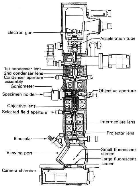
5 Cross-sectional view of a typical TEM


6 Holder Holder: Hold a standard size of grid upon which the sample is placed or a standard size of self-supporting specimen. Gatan 626 Gatan/Oxford CT3500

7 Stage/Goniometer Stage/Goniometer: Bring the region of interest into the path of the electron beam. Top entry Side entry
8 Elements in Illumination and Imaging Systems Gun Lenses Stigmators Deflection coils Apertures Illumination System Gun C1 C2 C3 Mini-condenser Condenser Gun Beam C1 C2 C3 Imaging System Objective Diffraction Intermediate Projector Objective Diffraction Image Objective Selected-area

9 System status
10 Elements in Electron Optics Gun Lenses Stigmators Deflection coils Apertures Holder and stage Recording media

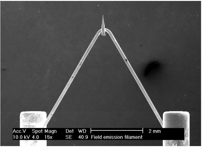
11 Electron Source W LaB 6 FEG
12 Some features of electron sources

13 Electromagnetic spectrum Electron wavelengths () Å at 100kV, Å at 120kV, Å at 200 kv, Å at 300 kv compare with wavelength of light: Å or X-rays: 1.5 Å for Cu K 1 Å synchrotron radiation diffraction limit for resolution of any optical system: D = /2
14 Elements in Electron Optics Gun Lenses Stigmators Deflection coils Apertures Holder and stage Recording media
15 Electromagnetic lenses Condenser (C1, C2, C3) Mini-Condenser Objective Diffraction Intermediate Projector (P1, P2)
16 Focal length of Electromagnetic lens f 2 K( U /( IN ) ) f = focal length, K = lens constant, U = voltage, I = current, N is the number of turns in the magnet coil. electromagnetic lens: can change focal length by changing current glass lens: change focus by moving specimen up and down change magnification by switching lenses
17 Condenser lens C1 Function: Determines the demagnification (size reduction) of the electron source onto the specimen and thus the spot size. How to adjust: change spotsize Spotsize index: 1-11 (FEI) Microprobe vs nanoprobe mode
18 Condenser lens C2 (C2/C3) Function: Determine how strongly the beam is focused onto the specimen and the convergence angle of the beam. How to adjust: Intensity knob Tecnai series (C2): Intensity Titan series (C2/C3): Illuminated area C2 lens has weak excitation and long focal length, why?
19 Parallel beam operation in a TEM C1, C2 control the beam size on the specimen. Using C2 to refocus the beam before C3 results in a more coherent beam. Front focal plane of C3 C3 (A) using just the C1 and an underfocused C2 lens. (B) using the C1 and C2 lenses to image the source at the front focal plane of C3.
20 Objective lens Function: Image formation Image focus in HM / Diffraction focus in LAD How to adjust: Focus knob


21 Conventional objective lens Objective lens design Riecke-Ruska design of symmetrical condenser-objective lens

22 Mini-condenser lens Function: produce a wide field of view and coherent illumination on the specimen in Microprobe mode. TWIN-lens design (A) Microprobe mode (B) Nanoprobe mode
23 Types of objective lens JEOL: URP, HRP, HTP, CRP, HCP FEI: Bio-TWIN, TWIN, C-TWIN, S-TWIN, X-TWIN, U-TWIN

24 Tecnai F20 with different obj. lens types


25 Magnetic lenses like Glass lenses are governed by Newton s lens equation a b and M b v f M ; M ; M a u u f l f f
26 How to set defocus? Defocus = u real u ideal <0, underfocus =0, in-focus >0, overfocus Underfocus is preferred for HREM/Cryo-EM Two methods to set an underfocus value: Reduce objective lens current (Turn focus knob counterclockwise) Reduce z-height f 2 K( U /( IN ) )

27 Lorentz lens For magnetic structure of the specimen
28 Diffraction lens Function: Diffraction focus in D / Image focus in LM How to adjust: Focus knob
29 Intermediate lens Function: Intermediate (Magnification, Imaging <-> Diffraction) How to adjust: Imaging Diffraction; Magnification knob
30 Imaging vs Diffraction
31 Optical modes Imaging: LM, HM (M, SA, Mh) Diffraction: LAD, D Imaging Diffraction LM LM LAD HM M D SA Mh
32 Projection lenses (P1, P2) Function: Magnification How to adjust: Magnification knob
33 Function of electromagnetic lenses Condenser (Beam focus) Objective (Image focus in HM / Diffraction focus in LAD) Diffraction (Diffraction focus in D / Image focus in LM) Intermediate (Magnification, Imaging <-> Diffraction) Projector (Magnification)
34 Elements in Electron Optics Gun Lenses Stigmators Deflection coils Apertures Holder and stage Recording media
35 Astigmatism Astigmatism occurs when a lens does not have perfect cylindrical symmetry. This may be by design, or due to manufacturing error. ra f A
36 Function of stigmators Condenser stigmator: Make the focused beam circular. Objective stigmator: Correct astigmatism in the HM (MI, SA, Mh) image. Correct astigmatism in the low-angle diffraction (LAD) pattern. Diffraction stigmator: Correct astigmatism in the LM image. Correct astigmatism in the diffraction (D) pattern.


37 Correction of astigmatism Condenser Objective Diffraction Before correction After correction
38 Elements in Electron Optics Gun Lenses Stigmators Deflection coils Apertures Holder and stage Recording media

39 Deflector coils A deflection coil is a set of coils on either side of the electron beam. The beam can be deflected into any direction by a suitable combination of x and y. Double deflection coils: The deflection coils are always mounted in sets of two above another. Double deflection coils are capable of two completely independent actions, a tilt and a shift.

40 Pivot points Tilt and shift actions by double deflection coils should be decoupled.
41 Type of Deflector coils Gun coils (Gun tilt / shift) Beam coils (Beam shift / tilt) Image coils (Image shift / Diffraction shift)
42 Elements in Electron Optics Gun Lenses Stigmators Deflection coils Apertures Holder and stage Recording media
43 Location of apertures C1 aperture Below C1 lens C2 aperture Below C2 lens Objective aperture: Back-focal plane of obj. lens SA aperture: Image plane of obj. lens
44 Function of apertures C1 aperture (Normally don t touch) Limit beam illuminated area C2 aperture Limit beam illuminated area Objective aperture Contrast forming (HM) Area selection (LM) SA aperture (Normally don t touch for phase contrast imaging) Contrast forming (LM) Area selection (HM) Only C2 and objective aperture can be adjusted on T12.
45 Summary: role of some elements changed with EM modes Objective lens: Image focus in HM / Diffraction focus in LAD Diffraction lens: Diffraction focus in D / Image focus in LM Objective stigmator: Correct astigmatism in the HM (MI, SA, Mh) image. Correct astigmatism in the low-angle diffraction (LAD) pattern. Diffraction stigmator: Correct astigmatism in the LM image. Correct astigmatism in the diffraction (D) pattern. Contrast aperture HM: Objective aperture LM: SA aperture Diffraction aperture HM: SA aperture LM: Objective aperture
46 Recording media Film Imaging plate CCD (Charge coupled device) Pseudo-CMOS based detector Direct electron detector
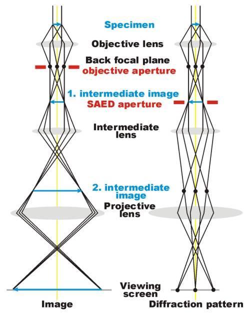
47 Imaging vs Diffraction
48 Modes of Operation of a TEM Diffraction Selected Area Electron Diffraction (SAED) Convergent-Beam Electron Diffraction (CBED) Imaging Mass-thickness contrast Diffraction contrast a) Bright-Field (BF) b) Dark-Field (DF) Phase contrast (HREM)

49 Electron diffraction Diffraction pattern locates at the back focal plane of the objective lens. Bragg angles are small. The diameter of the Ewald sphere is very large compared to the size of the unit cell in the reciprocal lattice. Lenses are able to focus the diffraction pattern and to change the camera length, which is equivalent to moving the film in an x-ray experiment.
50 Bragg s law 2d sin

51 Ewald Sphere 薄片样品使得倒易点变成倒易杆 和倒易矢相比, 电子波长非常短导致波矢很大, 因此倒易球半径非常大
52 SAED

53 Spot patterns Spot patterns corresponding to single-crystal diffraction

54 Ring patterns Ring patterns corresponding to powder diffraction from multiple crystals with a variable orientation
55 Diffraction with parallel illumination and conical illumination Parallel Beam Convergent beam

56 SAED vs CBED
![CBED Pattern CBED diffraction pattern from [111] Si](/docs-images/96/128700367/images/57-0.jpg "obtained at low (main pattern) and high (inset)")
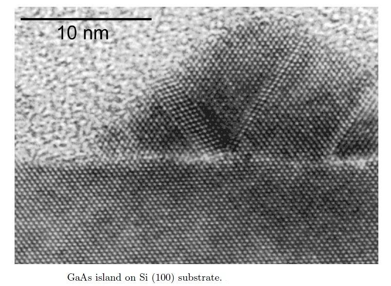
57 CBED Pattern CBED diffraction pattern from [111] Si obtained at low (main pattern) and high (inset) camera-lengths.
58 Image contrasts in TEM Mass-thickness contrast Scattering is dependent upon Z / Eo (Rutherford cross section) and the mean free path (specimen thickness). Diffraction contrast (BF, DF) Crystals and ordered materials diffract electrons at different angles. Phase Contrast (HREM) Constructive / destructive interference from the transmitted electrons gives rise to contrast. Z-contrast - scattering angle is highly dependent upon Z image electrons scattered at high angles
59 Mass-thickness contrast
60 Modes of Operation of a TEM Diffraction Selected Area Electron Diffraction (SAED) Convergent-Beam Electron Diffraction (CBED) Imaging Mass-thickness contrast Diffraction contrast a) Bright-Field (BF) b) Dark-Field (DF) Phase contrast (HREM) *Diffraction related
61 Diffraction contrast vs phase contrast Objective aperture
62 Diffraction contrast BF DF P.B. Hirsch, et al., Electron microscopy of thin crystals, 1993
63 DF

64 BF SAED DF
65 Application of Phase Contrast HREM Cryo-EM
66 HREM

67 Cryo-EM image
 0 ) dz (a) is the 3D Coulomb potential distribution within the object.")
68 Phase shift of wave behind object, where Phase shift of wave behind object with thickness t: t 0 2 ( k k 1 1 2meV 2me( V C( r)) 2 2 k0 ( ) is wave vector in vacuum, k ( ) 2 2 is wave vector in the object. V is acceleration voltage, and C(r) 0 ) dz (a) is the 3D Coulomb potential distribution within the object. (a) Can be written as, where ( x, y) ( x, y) C( r) dz V t 0 is projection of potential distribution Wavelength change C 1 C 0 Iso-phase lines
69 Weak phase object approximation Pure phase object: Transmission function: )), ( ), ( exp( ), ( y x u y x i y x q )), ( exp( ), ( y x i y x q... ), ( 2 1 ), ( y x y x i Weak phase object approximation: ), ( 1 ), ( y x i y x q
70 Observed contrast Transmission function: q( x, y) 1i ( x, y) After the object: Q( u, v) ( u, v) i( u, v) Apply CTF A( u, v)exp( i ( u, v)) : ( u, v) i( u, v) A( u, v)cos ( u, v) ( u, v) A( u, v)sin ( u, v) ( x) f ( x) ( x) f (0), and A(0,0) 1, (0,0) 0, [Note because ( u, v ) A( u, v )exp( i( u, v )) ( u, v )] Exit wave function: ( x, y) 1i ( x, y) ( A( u, v)cos( ( u, v))) ( x, y) ( A( u, v)sin( ( u, v))) Observed contrast: c( x, y) ( x, y) *( x, y) 1 2 ( x, y) ( A( u, v)sin( ( u, v))) ( ( x, y) ( A( u, v)sin( ( u, v)))) ( ( x, y) ( A( u, v)cos( ( u, v)))) 2 ( x, y) ( A( u, v)sin( ( u, v))) Corresponding power spectrum: C( u, v) 2 ( u, v) A( u, v)sin( ( u, v)) 2
71 Wave aberration function χ(μ,ν) Because astigmatism can be corrected, ) )]( sin 2( 2 [ ) ( 2 ), ( v u z z v u C v u a s Contributions: Spherical aberration Defocus Astigmatism ) ( ) ( 2 ), ( v u z v u C v u s k z k C s where, v u k
72 Envelope function A( u, v) R( u, v) E( u, v) Aperture function: 1 R( u, v) 0 for 0 elsewhere 2 2, where ( u v ), 0 is the angle 1 2 corresponding to the radius of the objective aperture Compound envelope function: E( u, v ) E ( u, v ) E ( u, v ) e i E e ( u, v ) : envelope function due to energy spread E i ( u, v ) : envelope function due to partially coherent illumination
73 E e ( u, v ) : envelope function due to energy spread Due to chromatic aberration, E e ( u, v) exp[ c ( u v exp[ c k ] 2 where c C c ( E) E 2 2 ) 2 ] ( V ) V 2 ( I) I 2
74 E i ( u, v ) :envelopefunction due topartially coherent illumination Spatial coherence (lateral coherence, transverse coherence) Due to finite source size, 2 E ( u, v) exp[ a i E 2 1 k0 for a Gaussian source distribution F( k0) exp( ) 2 2 a 2 c 3 ( C k for a top hat distribution s 3 zk) F 2 ] 1 ) a J1[2a c( Cs k zk)] u, v) 2 3 [2a ( C k zk)] i ( 3 c s envelope function due to partially coherent illumination for k c a c a c 2 0 c ( k 0 c elsewhere, with J 1 denoting the first-order Bessel function. (Notethat 3 C s k 3 zk is the gradient of the wave aberration function)
75 Point resolution vs Information limit Point resolution: 1.7 Å Information limit: 0.8 Å
76 q( x, y) exp( i ( x, y)) Amplitude contrast => C( u, v) 2 ( u, v) A( u, v)sin( ( u, v)) q( x, y) exp( i ( x, y) u( x, y)) => C( u, v) 2 ( u, v) A( u, v)[sin( ( u, v)) Q( u, v)cos( ( u, v))] It is assumed U( u, v) Q( u, v) ( u, v) (1) the same for all atoms in the specimen; (2) constant within the small spatial frequency range of practical interest in most cryo-em applications C s = 2 mm; Q = 0.15; Δz = -0.9 μm (solid line) Δz = -1.5 μm (dotted line) (a) Zeros shifts toward higher radii (b) CTF starts off with a nonzero term
NANO 703-Notes. Chapter 9-The Instrument
 1 Chapter 9-The Instrument Illumination (condenser) system Before (above) the sample, the purpose of electron lenses is to form the beam/probe that will illuminate the sample. Our electron source is macroscopic
ELECTRON MICROSCOPY. 13:10 16:00, Oct. 6, 2008 Institute of Physics, Academia Sinica. Tung Hsu
 ELECTRON MICROSCOPY 13:10 16:00, Oct. 6, 2008 Institute of Physics, Academia Sinica Tung Hsu Department of Materials Science and Engineering National Tsing Hua University Hsinchu 300, TAIWAN Tel. 03-5742564
Chapter 2 Instrumentation for Analytical Electron Microscopy Lecture 7. Chapter 2 CHEM Fall L. Ma
 Chapter 2 Instrumentation for Analytical Electron Microscopy Lecture 7 Outline Electron Sources (Electron Guns) Thermionic: LaB 6 or W Field emission gun: cold or Schottky Lenses Focusing Aberration Probe
Tecnai on-line help manual --
 Tecnai on-line help Alignments 1 Tecnai on-line help manual -- Alignments Table of Contents 1 Alignments in the Tecnai microscope...5 2 Alignment procedures...6 3 Introduction to electron optics...11 3.1
Transmission Electron Microscopy 9. The Instrument. Outline
 Transmission Electron Microscopy 9. The Instrument EMA 6518 Spring 2009 02/25/09 Outline The Illumination System The Objective Lens and Stage Forming Diffraction Patterns and Images Alignment and Stigmation
ELECTRON MICROSCOPY. 14:10 17:00, Apr. 3, 2007 Department of Physics, National Taiwan University. Tung Hsu
 ELECTRON MICROSCOPY 14:10 17:00, Apr. 3, 2007 Department of Physics, National Taiwan University Tung Hsu Department of Materials Science and Engineering National Tsinghua University Hsinchu 300, TAIWAN
Introduction to Transmission Electron Microscopy (Physical Sciences)
") Introduction to Transmission Electron Microscopy (Physical Sciences) Centre for Advanced Microscopy Program 9:30 10:45 Lecture 1 Basics of TEM 10:45 11:00 Morning tea 11:00 12:15 Lecture 2 Diffraction
Introduction to Transmission Electron Microscopy (Physical Sciences) Centre for Advanced Microscopy Program 9:30 10:45 Lecture 1 Basics of TEM 10:45 11:00 Morning tea 11:00 12:15 Lecture 2 Diffraction
Introduction to Electron Microscopy
 Introduction to Electron Microscopy Prof. David Muller, dm24@cornell.edu Rm 274 Clark Hall, 255-4065 Ernst Ruska and Max Knoll built the first electron microscope in 1931 (Nobel Prize to Ruska in 1986)
A few concepts in TEM and STEM explained
 A few concepts in TEM and STEM explained Martin Ek November 23, 2011 1 Introduction This is a collection of short, qualitative explanations of key concepts in TEM and STEM. Most of them are beyond what
Transmissions Electron Microscopy (TEM)
") Transmissions Electron Microscopy (TEM) Basic principles Diffraction Imaging Specimen preparation A.E. Gunnæs MENA3100 V17 TEM is based on three possible set of techniqes Diffraction From regions down
Transmissions Electron Microscopy (TEM) Basic principles Diffraction Imaging Specimen preparation A.E. Gunnæs MENA3100 V17 TEM is based on three possible set of techniqes Diffraction From regions down
Scanning electron microscope
 Scanning electron microscope 6 th CEMM workshop Maja Koblar, Sc. Eng. Physics Outline The basic principle? What is an electron? Parts of the SEM Electron gun Electromagnetic lenses Apertures Chamber and
--> Buy True-PDF --> Auto-delivered in 0~10 minutes. JY/T
 Translated English of Chinese Standard: JY/T011-1996 www.chinesestandard.net Sales@ChineseStandard.net INDUSTRY STANDARD OF THE JY PEOPLE S REPUBLIC OF CHINA General rules for transmission electron microscopy
Cs-corrector. Felix de Haas
 Cs-corrector. Felix de Haas Content Non corrector systems Lens aberrations and how to minimize? Corrector systems How is it done? Lens aberrations Spherical aberration Astigmatism Coma Chromatic Quality
MSE 460 TEM Lab 2: Basic Alignment and Operation of Microscope
 MSE 460 TEM Lab 2: Basic Alignment and Operation of Microscope Last updated on 1/8/2018 Jinsong Wu, jinsong-wu@northwestern.edu Aims: The aim of this lab is to familiarize you with basic TEM alignment
High Resolution Transmission Electron Microscopy (HRTEM) Summary 4/11/2018. Thomas LaGrange Faculty Lecturer and Senior Staff Scientist
 Summary 4/11/2018. Thomas LaGrange Faculty Lecturer and Senior Staff Scientist") Thomas LaGrange Faculty Lecturer and Senior Staff Scientist High Resolution Transmission Electron Microscopy (HRTEM) Doctoral Course MS-637 April 16-18th, 2018 Summary Contrast in TEM images results from
Thomas LaGrange Faculty Lecturer and Senior Staff Scientist High Resolution Transmission Electron Microscopy (HRTEM) Doctoral Course MS-637 April 16-18th, 2018 Summary Contrast in TEM images results from
Transmission electron Microscopy
 Transmission electron Microscopy Image formation of a concave lens in geometrical optics Some basic features of the transmission electron microscope (TEM) can be understood from by analogy with the operation
STEM alignment procedures
 STEM alignment procedures Step 1. ASID alignment mode 1. Write down STD for TEM, and then open the ASID control window from dialogue. Also, start Simple imager viewer program on the Desktop. 2. Click on
Introduction: Why electrons?
 Introduction: Why electrons? 1 Radiations Visible light X-rays Electrons Neutrons Advantages Not very damaging Easily focused Eye wonderful detector Small wavelength (Angstroms) Good penetration Small
S200 Course LECTURE 1 TEM
 S200 Course LECTURE 1 TEM Development of Electron Microscopy 1897 Discovery of the electron (J.J. Thompson) 1924 Particle and wave theory (L. de Broglie) 1926 Electromagnetic Lens (H. Busch) 1932 Construction
NanoSpective, Inc Progress Drive Suite 137 Orlando, Florida
 TEM Techniques Summary The TEM is an analytical instrument in which a thin membrane (typically < 100nm) is placed in the path of an energetic and highly coherent beam of electrons. Typical operating voltages
ELECTRON MICROSCOPY. 09:10 12:00, Oct. 27, 2006 Institute of Physics, Academia Sinica. Tung Hsu
 ELECTRON MICROSCOPY 09:10 12:00, Oct. 27, 2006 Institute of Physics, Academia Sinica Tung Hsu Department of Materials Science and Engineering National Tsinghua University Hsinchu 300, TAIWAN Tel. 03-5742564
FEI Falcon Direct Electron Detector. Best Practice Document
 FEI Falcon Direct Electron Detector Best Practice Document 2 1. Introduction FEI Falcon Direct Electron Detector Best Practice Application Guide The FEI Falcon Detector is based on direct electron detection
No part of this material may be reproduced without explicit written permission.
 This material is provided for educational use only. The information in these slides including all data, images and related materials are the property of : Robert M. Glaeser Department of Molecular & Cell
Full-screen mode Popup controls. Overview of the microscope user interface, TEM User Interface and TIA on the left and EDS on the right
 Quick Guide to Operating FEI Titan Themis G2 200 (S)TEM: TEM mode Susheng Tan Nanoscale Fabrication and Characterization Facility, University of Pittsburgh Office: M104/B01 Benedum Hall, 412-383-5978,
MSE 595T Transmission Electron Microscopy. Laboratory III TEM Imaging - I
 MSE 595T Basic Transmission Electron Microscopy TEM Imaging - I Purpose The purpose of this lab is to: 1. Make fine adjustments to the microscope alignment 2. Obtain a diffraction pattern 3. Obtain an
GBS765 Hybrid methods
 GBS765 Hybrid methods Lecture 3 Contrast and image formation 10/20/14 4:37 PM The lens ray diagram Magnification M = A/a = v/u and 1/u + 1/v = 1/f where f is the focal length The lens ray diagram So we
1.2. Make sure the viewing screen is covered (exposure to liquid N 2 may cause it to crack).
.") FEI Tecnai F20 S/TEM: imaging in TEM mode Nicholas G. Rudawski ngr@ufl.edu (805) 252-4916 (352) 392-3077 Last updated: 01/21/18 1. Filling the cold trap (if needed) 1.1. Prior to use, the cold trap needs
FEI Tecnai F20 S/TEM: imaging in TEM mode Nicholas G. Rudawski ngr@ufl.edu (805) 252-4916 (352) 392-3077 Last updated: 01/21/18 1. Filling the cold trap (if needed) 1.1. Prior to use, the cold trap needs
Chapter 4 Imaging Lecture 17
 Chapter 4 Imaging Lecture 17 d (110) Imaging Imaging in the TEM Diffraction Contrast in TEM Image HRTEM (High Resolution Transmission Electron Microscopy) Imaging STEM imaging Imaging in the TEM What is
Nanotechnology and material science Lecture V
 Most widely used nanoscale microscopy. Based on possibility to create bright electron beam with sub-nm spot size. History: Ernst Ruska (1931), Nobel Prize (1986) For visible light λ=400-700nm, for electrons
Chapter Ray and Wave Optics
 109 Chapter Ray and Wave Optics 1. An astronomical telescope has a large aperture to [2002] reduce spherical aberration have high resolution increase span of observation have low dispersion. 2. If two
VISUAL PHYSICS ONLINE DEPTH STUDY: ELECTRON MICROSCOPES
 VISUAL PHYSICS ONLINE DEPTH STUDY: ELECTRON MICROSCOPES Shortly after the experimental confirmation of the wave properties of the electron, it was suggested that the electron could be used to examine objects
Indiana University JEM-3200FS
 Indiana University JEM-3200FS Installation Specification Model: JEM 3200FS Serial Number: EM 15000013 Objective Lens Configuration: High Resolution Pole Piece (HRP) JEOL Engineer: Michael P. Van Etten
MSE 460 TEM Lab 4: Bright/Dark Field Imaging Operation
 MSE 460 TEM Lab 4: Bright/Dark Field Imaging Operation Last updated on 1/8/2018 Jinsong Wu, jinsong-wu@northwestern.edu Aims: The aim of this lab is to familiarize you with bright/dark field imaging operation.
Scanning electron microscope
 Scanning electron microscope 5 th CEMM workshop Maja Koblar, Sc. Eng. Physics Outline The basic principle? What is an electron? Parts of the SEM Electron gun Electromagnetic lenses Apertures Detectors
Instructions for Tecnai a brief start up manual
 Instructions for Tecnai a brief start up manual Version 3.0, 8.12.2015 Manual of Tecnai 12 transmission electron microscope located at Aalto University's Nanomicroscopy Center. More information of Nanomicroscopy
EE119 Introduction to Optical Engineering Spring 2003 Final Exam. Name:
 EE119 Introduction to Optical Engineering Spring 2003 Final Exam Name: SID: CLOSED BOOK. THREE 8 1/2 X 11 SHEETS OF NOTES, AND SCIENTIFIC POCKET CALCULATOR PERMITTED. TIME ALLOTTED: 180 MINUTES Fundamental
2.Components of an electron microscope. a) vacuum systems, b) electron guns, c) electron optics, d) detectors. Marco Cantoni 021/
 vacuum systems, b) electron guns, c) electron optics, d) detectors. Marco Cantoni 021/") 2.Components of an electron microscope a) vacuum systems, b) electron guns, c) electron optics, d) detectors, 021/693.48.16 Centre Interdisciplinaire de Microscopie Electronique CIME Summary Electron propagation
2.Components of an electron microscope a) vacuum systems, b) electron guns, c) electron optics, d) detectors, 021/693.48.16 Centre Interdisciplinaire de Microscopie Electronique CIME Summary Electron propagation
2 How to operate the microscope/obtain an image
 Morgagni Operating Instructions 50079 010912 2-1 2 ow to operate the microscope/obtain an image 2.1 Starting the microscope 2.1.1 Starting the microscope with several manually-operated steps 1. Turn on
Chapter 1. Basic Electron Optics (Lecture 2)
") Chapter 1. Basic Electron Optics (Lecture 2) Basic concepts of microscope (Cont ) Fundamental properties of electrons Electron Scattering Instrumentation Basic conceptions of microscope (Cont ) Ray diagram
Chapter 1. Basic Electron Optics (Lecture 2) Basic concepts of microscope (Cont ) Fundamental properties of electrons Electron Scattering Instrumentation Basic conceptions of microscope (Cont ) Ray diagram
Phase plates for cryo-em
 Max Planck Institute of Biochemistry Martinsried, Germany MAX PLANCK SOCIETY Phase plates for cryo-em Rado Danev Max Planck Institute of Biochemistry, Martinsried, Germany. EMBO course 2017, London, UK
Introduction to Light Microscopy. (Image: T. Wittman, Scripps)
") Introduction to Light Microscopy (Image: T. Wittman, Scripps) The Light Microscope Four centuries of history Vibrant current development One of the most widely used research tools A. Khodjakov et al. Major
Introduction to Light Microscopy (Image: T. Wittman, Scripps) The Light Microscope Four centuries of history Vibrant current development One of the most widely used research tools A. Khodjakov et al. Major
FYS 4340/FYS Diffraction Methods & Electron Microscopy. Lecture 9. Imaging Part I. Sandeep Gorantla. FYS 4340/9340 course Autumn
 FYS 4340/FYS 9340 Diffraction Methods & Electron Microscopy Lecture 9 Imaging Part I Sandeep Gorantla FYS 4340/9340 course Autumn 2016 1 Imaging 2 Abbe s principle of imaging Unlike with visible light,
SCANNING ELECTRON MICROSCOPY AND X-RAY MICROANALYSIS
 SCANNING ELECTRON MICROSCOPY AND X-RAY MICROANALYSIS Robert Edward Lee Electron Microscopy Center Department of Anatomy and Neurobiology Colorado State University P T R Prentice Hall, Englewood Cliffs,
1.3. Before loading the holder into the TEM, make sure the X tilt is set to zero and the goniometer locked in place (this will make loading easier).
.") JEOL 200CX operating procedure Nicholas G. Rudawski ngr@ufl.edu (805) 252-4916 1. Specimen loading 1.1. Unlock the TUMI system. 1.2. Load specimen(s) into the holder. If using the double tilt holder, ensure
JEOL 200CX operating procedure Nicholas G. Rudawski ngr@ufl.edu (805) 252-4916 1. Specimen loading 1.1. Unlock the TUMI system. 1.2. Load specimen(s) into the holder. If using the double tilt holder, ensure
Electron Sources, Optics and Detectors
 Thomas LaGrange, Ph.D. Faculty Lecturer and Senior Staff Scientist Electron Sources, Optics and Detectors TEM Doctoral Course MS-637 April 16 th -18 th, 2018 Summary Electron propagation is only possible
Nanotechnology in Consumer Products
 Nanotechnology in Consumer Products Advances in Transmission Electron Microscopy Friday, April 21, 2017 October 31, 2014 The webinar will begin at 1pm Eastern Time Click here to watch the webinar recording
1.1. In regular TEM imaging mode, find a region of interest and set it at eucentric height.
 JEOL 2010F operating procedure Covers operation in STEM mode (See separate procedures for operation in TEM mode and operation of EDS system) Nicholas G. Rudawski ngr@ufl.edu (805) 252-4916 NOTE: this operating
Introduction to Electron Microscopy-II
 Introduction to Electron Microscopy-II Prof. David Muller, dm24@cornell.edu Rm 274 Clark Hall, 255-4065 Ernst Ruska and Max Knoll built the first electron microscope in 1931 (Nobel Prize to Ruska in 1986)
Systems Biology. Optical Train, Köhler Illumination
 McGill University Life Sciences Complex Imaging Facility Systems Biology Microscopy Workshop Tuesday December 7 th, 2010 Simple Lenses, Transmitted Light Optical Train, Köhler Illumination What Does a
Microscope anatomy, image formation and resolution
 Microscope anatomy, image formation and resolution Ian Dobbie Buy this book for your lab: D.B. Murphy, "Fundamentals of light microscopy and electronic imaging", ISBN 0-471-25391-X Visit these websites:
Physics 431 Final Exam Examples (3:00-5:00 pm 12/16/2009) TIME ALLOTTED: 120 MINUTES Name: Signature:
 TIME ALLOTTED: 120 MINUTES Name: Signature:") Physics 431 Final Exam Examples (3:00-5:00 pm 12/16/2009) TIME ALLOTTED: 120 MINUTES Name: PID: Signature: CLOSED BOOK. TWO 8 1/2 X 11 SHEET OF NOTES (double sided is allowed), AND SCIENTIFIC POCKET CALCULATOR
Physics 431 Final Exam Examples (3:00-5:00 pm 12/16/2009) TIME ALLOTTED: 120 MINUTES Name: PID: Signature: CLOSED BOOK. TWO 8 1/2 X 11 SHEET OF NOTES (double sided is allowed), AND SCIENTIFIC POCKET CALCULATOR
Titan on-line help manual -- Working with a FEG
 1 manual -- Working with a FEG Table of Contents 1 FEG Safety... 2 1.1 The column valves... 2 2 FEG States... 2 3 Starting the FEG... 4 4 Shutting the FEG down... 6 5 FEG Design... 6 5.1 Electron source...
FEI Tecnai G 2 F20 Operating Procedures
 FEI Tecnai G 2 F20 Operating Procedures 1. Startup (1) Sign-up in the microscope log-sheet. Please ensure you have written an account number for billing. (2) Log in to the computer: Login to your account
AQA P3 Topic 1. Medical applications of Physics
 AQA P3 Topic 1 Medical applications of Physics X rays X-ray properties X-rays are part of the electromagnetic spectrum. X-rays have a wavelength of the same order of magnitude as the diameter of an atom.
Contrast transfer. Contrast transfer and CTF correction. Lecture 6 H Saibil
 Lecture 6 H Saibil Contrast transfer Contrast transfer and CTF correction The weak phase approximation Contrast transfer function Determining defocus CTF correction methods Image processing for cryo microscopy
Introduction of New Products
 Field Emission Electron Microscope JEM-3100F For evaluation of materials in the fields of nanoscience and nanomaterials science, TEM is required to provide resolution and analytical capabilities that can
2. Raise HT to 200kVby following the procedure explained in 1.6.
 JEOL 2100 MANUAL Quick check list 1. If needed, fill the reservoir with LN2 2. Raise HT to 200kVby following the procedure explained in 1.6. 3. Insert specimen holder into TEM (Insert holder in airlock,
25 cm. 60 cm. 50 cm. 40 cm.
 Geometrical Optics 7. The image formed by a plane mirror is: (a) Real. (b) Virtual. (c) Erect and of equal size. (d) Laterally inverted. (e) B, c, and d. (f) A, b and c. 8. A real image is that: (a) Which
Lecture 2: Geometrical Optics. Geometrical Approximation. Lenses. Mirrors. Optical Systems. Images and Pupils. Aberrations.
 Lecture 2: Geometrical Optics Outline 1 Geometrical Approximation 2 Lenses 3 Mirrors 4 Optical Systems 5 Images and Pupils 6 Aberrations Christoph U. Keller, Leiden Observatory, keller@strw.leidenuniv.nl
OPTICAL SYSTEMS OBJECTIVES
 101 L7 OPTICAL SYSTEMS OBJECTIVES Aims Your aim here should be to acquire a working knowledge of the basic components of optical systems and understand their purpose, function and limitations in terms
Recent results from the JEOL JEM-3000F FEGTEM in Oxford
 Recent results from the JEOL JEM-3000F FEGTEM in Oxford R.E. Dunin-Borkowski a, J. Sloan b, R.R. Meyer c, A.I. Kirkland c,d and J. L. Hutchison a a b c d Department of Materials, Parks Road, Oxford OX1
Image Formation. Light from distant things. Geometrical optics. Pinhole camera. Chapter 36
 Light from distant things Chapter 36 We learn about a distant thing from the light it generates or redirects. The lenses in our eyes create images of objects our brains can process. This chapter concerns
This document assumes the user is already familiar with basic operation of the instrument in TEM mode and use of the Microscope Control interface.
 FEI Tecnai F20 S/TEM: imaging in STEM mode Nicholas G. Rudawski ngr@ufl.edu (805) 252-4916 (352) 392-3077 Last updated: 05/10/18 This document assumes the user is already familiar with basic operation
Low Voltage Electron Microscope
 LVEM5 Low Voltage Electron Microscope Nanoscale from your benchtop LVEM5 Delong America DELONG INSTRUMENTS COMPACT BUT POWERFUL The LVEM5 is designed to excel across a broad range of applications in material
Electron
 Electron 1897: Sir Joseph John Thomson (1856-1940) discovered corpuscles small particles with a charge-to-mass ratio over 1000 times greater than that of protons. Plum pudding model : electrons in a sea
EE119 Introduction to Optical Engineering Fall 2009 Final Exam. Name:
 EE119 Introduction to Optical Engineering Fall 2009 Final Exam Name: SID: CLOSED BOOK. THREE 8 1/2 X 11 SHEETS OF NOTES, AND SCIENTIFIC POCKET CALCULATOR PERMITTED. TIME ALLOTTED: 180 MINUTES Fundamental
INTRODUCTION TO ABERRATIONS IN OPTICAL IMAGING SYSTEMS
 INTRODUCTION TO ABERRATIONS IN OPTICAL IMAGING SYSTEMS JOSE SASIÄN University of Arizona ШШ CAMBRIDGE Щ0 UNIVERSITY PRESS Contents Preface Acknowledgements Harold H. Hopkins Roland V. Shack Symbols 1 Introduction
Lecture 2: Geometrical Optics. Geometrical Approximation. Lenses. Mirrors. Optical Systems. Images and Pupils. Aberrations.
 Lecture 2: Geometrical Optics Outline 1 Geometrical Approximation 2 Lenses 3 Mirrors 4 Optical Systems 5 Images and Pupils 6 Aberrations Christoph U. Keller, Leiden Observatory, keller@strw.leidenuniv.nl
A Tutorial on Electron Microscopy
 A Tutorial on Electron Microscopy Jian-Min (Jim) Zuo Mat. Sci. Eng. and Seitz-Materials Research Lab., UIUC Outline of This Tutorial I. Science and opportunities of electron microscopy II. The basic TEM,
ELECTRON MICROSCOPY AN OVERVIEW
 ELECTRON MICROSCOPY AN OVERVIEW Anjali Priya 1, Abhishek Singh 2, Nikhil Anand Srivastava 3 1,2,3 Department of Electrical & Instrumentation, Sant Longowal Institute of Engg. & Technology, Sangrur, India.
Mirrors, Lenses &Imaging Systems
 Mirrors, Lenses &Imaging Systems We describe the path of light as straight-line rays And light rays from a very distant point arrive parallel 145 Phys 24.1 Mirrors Standing away from a plane mirror shows
Properties of optical instruments. Visual optical systems part 2: focal visual instruments (microscope type)
") Properties of optical instruments Visual optical systems part 2: focal visual instruments (microscope type) Examples of focal visual instruments magnifying glass Eyepieces Measuring microscopes from the
Properties of optical instruments Visual optical systems part 2: focal visual instruments (microscope type) Examples of focal visual instruments magnifying glass Eyepieces Measuring microscopes from the
INTRODUCTION THIN LENSES. Introduction. given by the paraxial refraction equation derived last lecture: Thin lenses (19.1) = 1. Double-lens systems
 = 1. Double-lens systems") Chapter 9 OPTICAL INSTRUMENTS Introduction Thin lenses Double-lens systems Aberrations Camera Human eye Compound microscope Summary INTRODUCTION Knowledge of geometrical optics, diffraction and interference,
Chapter 9 OPTICAL INSTRUMENTS Introduction Thin lenses Double-lens systems Aberrations Camera Human eye Compound microscope Summary INTRODUCTION Knowledge of geometrical optics, diffraction and interference,
EE119 Introduction to Optical Engineering Spring 2002 Final Exam. Name:
 EE119 Introduction to Optical Engineering Spring 2002 Final Exam Name: SID: CLOSED BOOK. FOUR 8 1/2 X 11 SHEETS OF NOTES, AND SCIENTIFIC POCKET CALCULATOR PERMITTED. TIME ALLOTTED: 180 MINUTES Fundamental
Lens Design I. Lecture 3: Properties of optical systems II Herbert Gross. Summer term
 Lens Design I Lecture 3: Properties of optical systems II 205-04-8 Herbert Gross Summer term 206 www.iap.uni-jena.de 2 Preliminary Schedule 04.04. Basics 2.04. Properties of optical systrems I 3 8.04.
2.Components of an electron microscope. a) vacuum systems, b) electron guns, c) electron optics, d) detectors. Marco Cantoni, 021/
 vacuum systems, b) electron guns, c) electron optics, d) detectors. Marco Cantoni, 021/") 2.Components of an electron microscope a) vacuum systems, b) electron guns, c) electron optics, d) detectors Marco Cantoni, 021/693.48.16 Centre Interdisciplinaire de Microscopie Electronique CIME MSE-603
2.Components of an electron microscope a) vacuum systems, b) electron guns, c) electron optics, d) detectors Marco Cantoni, 021/693.48.16 Centre Interdisciplinaire de Microscopie Electronique CIME MSE-603
Opti 415/515. Introduction to Optical Systems. Copyright 2009, William P. Kuhn
 Opti 415/515 Introduction to Optical Systems 1 Optical Systems Manipulate light to form an image on a detector. Point source microscope Hubble telescope (NASA) 2 Fundamental System Requirements Application
Chapter 36: diffraction
 Chapter 36: diffraction Fresnel and Fraunhofer diffraction Diffraction from a single slit Intensity in the single slit pattern Multiple slits The Diffraction grating X-ray diffraction Circular apertures
Lab 05: Transmission Electron Microscopy
 Lab 05: Transmission Electron Microscopy Author: Mike Nill Alex Bryant Contents 1 Introduction 2 1.1 Imaging Modes....................................... 2 1.2 Electromagnetic Lenses..................................
CS-TEM vs CS-STEM. FEI Titan CIME EPFL. Duncan Alexander EPFL-CIME
 CS-TEM vs CS-STEM Duncan Alexander EPFL-CIME 1 FEI Titan Themis @ CIME EPFL 60 300 kv Monochromator High brightness X-FEG Probe Cs-corrected: 0.7 Å @ 300 kv Image Cs-corrected: 0.7 Å @ 300 kv Super-X EDX
The Wave Nature of Light
 The Wave Nature of Light Physics 102 Lecture 7 4 April 2002 Pick up Grating & Foil & Pin 4 Apr 2002 Physics 102 Lecture 7 1 Light acts like a wave! Last week we saw that light travels from place to place
GEOMETRICAL OPTICS AND OPTICAL DESIGN
 GEOMETRICAL OPTICS AND OPTICAL DESIGN Pantazis Mouroulis Associate Professor Center for Imaging Science Rochester Institute of Technology John Macdonald Senior Lecturer Physics Department University of
EE-527: MicroFabrication
 EE-57: MicroFabrication Exposure and Imaging Photons white light Hg arc lamp filtered Hg arc lamp excimer laser x-rays from synchrotron Electrons Ions Exposure Sources focused electron beam direct write
Diffraction. Interference with more than 2 beams. Diffraction gratings. Diffraction by an aperture. Diffraction of a laser beam
 Diffraction Interference with more than 2 beams 3, 4, 5 beams Large number of beams Diffraction gratings Equation Uses Diffraction by an aperture Huygen s principle again, Fresnel zones, Arago s spot Qualitative
Modulation Transfer Function
 Modulation Transfer Function The Modulation Transfer Function (MTF) is a useful tool in system evaluation. t describes if, and how well, different spatial frequencies are transferred from object to image.
Physics 3340 Spring Fourier Optics
 Physics 3340 Spring 011 Purpose Fourier Optics In this experiment we will show how the Fraunhofer diffraction pattern or spatial Fourier transform of an object can be observed within an optical system.
Introduction to Optical Modeling. Friedrich-Schiller-University Jena Institute of Applied Physics. Lecturer: Prof. U.D. Zeitner
 Introduction to Optical Modeling Friedrich-Schiller-University Jena Institute of Applied Physics Lecturer: Prof. U.D. Zeitner The Nature of Light Fundamental Question: What is Light? Newton Huygens / Maxwell
OPAC 202 Optical Design and Instrumentation. Topic 3 Review Of Geometrical and Wave Optics. Department of
 OPAC 202 Optical Design and Instrumentation Topic 3 Review Of Geometrical and Wave Optics Department of http://www.gantep.edu.tr/~bingul/opac202 Optical & Acustical Engineering Gaziantep University Feb
Topics 3b,c Electron Microscopy
 Topics 3b,c Electron Microscopy 1.0 Introduction and History 1.1 Characteristic Information 2.0 Basic Principles 2.1 Electron-Solid Interactions 2.2 Electromagnetic Lenses 2.3 Breakdown of an Electron
ECEN 4606, UNDERGRADUATE OPTICS LAB
 ECEN 4606, UNDERGRADUATE OPTICS LAB Lab 2: Imaging 1 the Telescope Original Version: Prof. McLeod SUMMARY: In this lab you will become familiar with the use of one or more lenses to create images of distant
b) (4) If you could look at a snapshot of the waves, how far apart in space are two successive positive peaks of the electric field?
 (4) If you could look at a snapshot of the waves, how far apart in space are two successive positive peaks of the electric field?") General Physics II Exam 3 - Chs. 22 25 - EM Waves & Optics October 20, 206 Name Rec. Instr. Rec. Time For full credit, make your work clear. Show formulas used, essential steps, and results with correct
General Physics II Exam 3 - Chs. 22 25 - EM Waves & Optics October 20, 206 Name Rec. Instr. Rec. Time For full credit, make your work clear. Show formulas used, essential steps, and results with correct
X rays X-ray properties Denser material = more absorption = looks lighter on the x-ray photo X-rays CT Scans circle cross-sectional images Tumours
 X rays X-ray properties X-rays are part of the electromagnetic spectrum. X-rays have a wavelength of the same order of magnitude as the diameter of an atom. X-rays are ionising. Different materials absorb
This document assumes the user is already familiar with basic operation of the instrument in TEM mode and use of the digital camera.
 FEI Tecnai F20 S/TEM: acquiring diffraction patterns Nicholas G. Rudawski ngr@ufl.edu (805) 252-4916 (352) 392-3077 Last updated: 10/18/17 This document assumes the user is already familiar with basic
Procedures for Performing Cryoelectron Microscopy on the FEI Sphera Microscope
 Procedures for Performing Cryoelectron Microscopy on the FEI Sphera Microscope The procedures given below were written specifically for the FEI Tecnai G 2 Sphera microscope. Modifications will need to
BEAM HALO OBSERVATION BY CORONAGRAPH
 BEAM HALO OBSERVATION BY CORONAGRAPH T. Mitsuhashi, KEK, TSUKUBA, Japan Abstract We have developed a coronagraph for the observation of the beam halo surrounding a beam. An opaque disk is set in the beam
 Telecentric Imaging Object space telecentricity stop source: edmund optics The 5 classical Seidel Aberrations First order aberrations Spherical Aberration (~r 4 ) Origin: different focal lengths for different
Exercises Advanced Optical Design Part 5 Solutions
 2014-12-09 Manuel Tessmer M.Tessmer@uni-jena.dee Minyi Zhong minyi.zhong@uni-jena.de Herbert Gross herbert.gross@uni-jena.de Friedrich Schiller University Jena Institute of Applied Physics Albert-Einstein-Str.
Phys 531 Lecture 9 30 September 2004 Ray Optics II. + 1 s i. = 1 f
 Phys 531 Lecture 9 30 September 2004 Ray Optics II Last time, developed idea of ray optics approximation to wave theory Introduced paraxial approximation: rays with θ 1 Will continue to use Started disussing
Low Voltage Electron Microscope. Nanoscale from your benchtop LVEM5. Delong America
 LVEM5 Low Voltage Electron Microscope Nanoscale from your benchtop LVEM5 Delong America DELONG INSTRUMENTS COMPACT BUT POWERFUL The LVEM5 is designed to excel across a broad range of applications in material
JEOL JEM 2010 TRAINING TRANSMISSION ELECTRON MICROSCOPE USER MANUAL
 JEOL JEM 2010 TRAINING TRANSMISSION ELECTRON MICROSCOPE USER MANUAL Version 5.1 EM Facility CMSE-SEF Massachusetts Institution of Technology TABLE OF CONTENTS 1. Specifications...2 1.1 Performance...2