Scanning electron microscope
|
|
|
- Hilary Richards
- 6 years ago
- Views:
Transcription
1 Scanning electron microscope 5 th CEMM workshop Maja Koblar, Sc. Eng. Physics
2 Outline The basic principle? What is an electron? Parts of the SEM Electron gun Electromagnetic lenses Apertures Detectors Electrons and their interactions with the specimen SEM settings and how we observe it on the image Voltage Current WD and apertures Scanning speed
3 What is it? By using a focused beam of electrons, we can see otherwise invisible worlds on the microscale and nanoscale. In LM: the specimen is unchanged by observation In EM: interaction can have more serious consequences (heated and chemical changes) SEM advantages over LM: Resolution at high magnification Depth of focus (field, depth) Microanalysis But must be vacuum compatible and conductive! (Images: ammrf) Resolution? The ability to distinguish closely spaced points as separate points. Magnification is the enlargement of an image, or portion of an image. In a SEM this is achieved by scanning a smaller area. In the images, the beam is indicated by arrows on a sample.
4 (Image: ammrf) Basic principle of SEM operation
5 What is an electron? Electrons are small subatomic particles (small and firm, like a ball). In the 1920 in Bell laboratories an experiment was made were the beam of electrons passed a double slit and was observed on the screen Ambiguity: a woman's face or a man playing a saxophone Quantum mechanics: Niels Bohr Wave particle duality Example: Analogy with a spinning coin. Image: getmedic.ru (Images: physics.stackexchange.com)
6 (Image: LEGO) Parts of the SEM Microscope (column and chamber), computer and other parts (vacuum system, water chilling system, microanalysis )
 condenser to shape the beam apertures to limit the beam scan coils to deflect the beam objective lenses to focus the beam")
7 Microscope column electron gun Gun aperture and alignment coils Gun isolation valve Faraday cup Aperture angle control lens In column energy filter (R-filter) condenser to shape the beam apertures to limit the beam scan coils to deflect the beam objective lenses to focus the beam (Image: JEOL)
8 Electron gun

9 Thermionic emission The components to produce an electron beam: an emitter (electrode W or LaB6) JSM-5800 a surrounding cathode (Wehnelt cylinder/ grid cap) an anode with a central hole. E = E w E F Emission current density Tungsten: J th = 3,4 A/cm 2 T = 2700 K, E w = 4,5 ev (Image: ammrf) LaB 6 : J th = 40 A/cm 2 T = 1800 K, E w = 2,5 ev (Image: Goldstein)
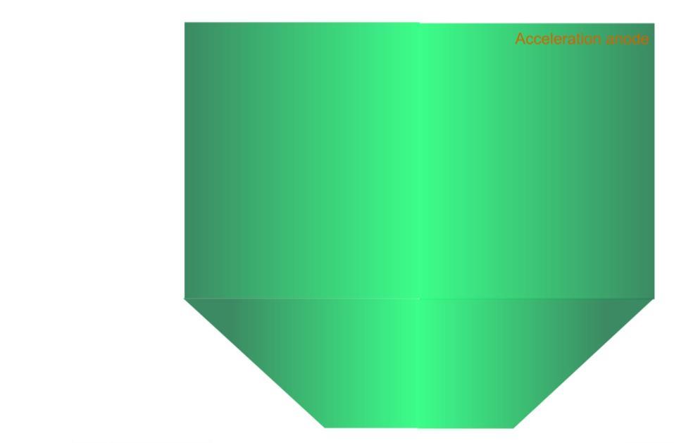
10 Field emission The FE gun consists of: Emitter cathode - tungsten with a very sharp point <100nm E w Cathode E w (SE) Vacuum Thermionic Suppresser anode (only Schottky field assisted thermionic emitter) Extraction anode (a very strong field at the tip >10 7 V/cm) Accelerating anode (final accelerating) E f for ZrO 2 /W E f for W Field emission nm
11 Quantum tunnelling 11


12 Quantum tunnelling 12


13 Schottky FEG (Image: tnw.tudelft) (Image: JEOL) (Image: JEOL)
14 Comparison of electron guns Emitter Type Thermionic Thermionic Schottky FEG cold FEG Cathode material W LaB 6 ZrO/W (100) W(310) Operating temperature [K] Cathode radius [nm] Effective source radius [nm] 2,800 1,900 1, ,000 10,000 < 1,000 < ,000 5, Emission current density [A/cm 2 ] ,300 17,000 Total emission current [µa] Normalized brightness [A/cm 2.sr.kV] 1 x x x x 10 7 Maximum probe current [na] Energy cathode [ev] Energy gun exit [ev] Beam noise [%] Emission current drift [%/h] < Operating vacuum hpa/mbar 1 < 1 x 10⁻⁵ < 1 x 10⁻⁶ < 1 x 10⁻⁹ < 1 x Typical Cathode life [h] 100 > 1000 > 5000 > 2000 Cathode regeneration not required not required not required every 6 to 8 hours Sensitivity to external influence minimal minimal low high (Table: tedpella)
15 Electromagnetic lens system Condenser lens, objective lens and scanning coils.
16 EM lenses Similar to glass lenses in optical microscopes. Main role of EM lenses is to demagnify the source of electrons to form a much smaller diameter probe. Two main lenses used in SEM: Condenser lenses Objective lenses (Images: ammrf)
17 EM lenses CONDENSER LENS The main role of the condenser lens is to control the size of the beam and determines the number of electrons in the beam which hit the sample. OBJECTIVE LENS Focuses electrons on the sample at the working distance. (Images: ammrf)

18 Apertures to limit the beam


.")

19 Apertures For ultra high resolution use the smallest 30 µm (smaller probe, low current, large depth of focus). For microanalysis use the largest 110 µm (observation at high currents, shallow depth of focus, higher statistics). For usual observation use 50 µm. To work with high probe current, but still good resolution use 70 µm. Needs to be changed regularly. 30 µm 50 µm 70 µm 110 µm
20 Sample chamber motorized stage (x,y,z,t,r) detectors RIBE EDS RBEI SEI GB LN2 LEI (Image: JEOL)


21 Pole piece EDS LEI EDS BEI SEI Cold trap RBEI stage stage Turbo pump JSM-7600F JSM-5800
22 Electrons and their interactions with the specimen But we will not talk about excitation, we will talk about ionization.
23 Interactions Electrons: Secondary (low energy) Backscattered (high energy) Transmitted Auger electrons Beam current SEM TEM Photons X-rays cathodoluminescence (Images: Low Voltage Electron Microscopy: Principles and Applications)
24 SEM signal Secondary electrons (SE) Backscattered electrons (BSE) Primary incident beam of electrons of sufficient energy, hits a surface (SEM) or passes through some material (TEM) and induces the emission of secondary particles.
25 Total electron yield: σ = δ + η SE yield (δ) the number of secondary electrons emitted per incident particle is called secondary emission yield BSE yield (η) the number of backscattered electrons emitted per incident particle is called backscattered emission yield
26 Signal Secondary electrons High resolution Strongly topography sensitive Little element sensitive Sensitive to charging Backscattered electrons Lower resolution Atomic number contrast in particular strong signal to heavy atoms Less sensitive to charging
 WD and apertures")
27 SEM settings Voltage (electrical potential) Consider as the spread or energy of electrons Typically 1-30 kv or kev Current (number of electrons/unit time (amps)) 1 coulomb ~ 6 x electrons 1 A = 1 C/s Typically from A to 10-9 A So 1 na~ 9 x 10 9 electrons/sec Beam voltage Gun emission current Beam current control (condensers) WD and apertures
28 Voltage (Images: ammrf)

29 Voltage 15 kv 5 kv
30 Probe current (Images: ammrf)


31 Probe current PC 8 0,35 na PC 6 0,08 na
32 Depth of focus The WD and the aperture impacts on the depth of field and resolution of the SEM image (Images: ammrf) High DOF: use smaller aperture and larger WD Low DOF: use bigger aperture and smaller WD

33 Imaging speed
 + integration (8)")
34 Photo 2 Fine (7/1) Fine (7/1) + integration (8)
35 What is the working distance? A. The seated distance between the microscopist and the microscope B. The distance from the specimen to the secondary electron detector C. The distance from the specimen to the objective lens pole piece D. The distance from the specimen to X-ray detector


36 JSM-5800 and JSM-7600F Different height of samples BSE on 5800 damaged!! BSE on 7600F carbon tape on it!! (Image: ammrf)
 use slow movement (x, y and z) under the objective lens!")
37 Magnetic samples A) minimal amount as possible! Bulk - less force Powder to avoid flying of the holder B) mount it very good! Use special holder C) use slow movement (x, y and z) under the objective lens! Turn on LM mode Be further away from the pol piece D) focus, stigmatizm very slowly!
38 Take home information The SEM works differently than LM But there are some similarities Why is it possible to image with electrons The wave particle duality and the scanning mode makes it possible Different parts of the SEM and what is the difference between them Why we have different types of electron gun (W, FE) How the electromagnetic lenses work and why magnetic samples are a problem Why we need Apertures Detectors Electrons and their interactions with the specimen and what kind of information we get from SE and BSE image SE yield BSE yield SEM settings and how we observe it on the image What is the difference in image depending on the Voltage Current WD and apertures Scanning speed

39

40 Next workshop on : - EDS, - WDS, - EBSD,
Scanning electron microscope
 Scanning electron microscope 6 th CEMM workshop Maja Koblar, Sc. Eng. Physics Outline The basic principle? What is an electron? Parts of the SEM Electron gun Electromagnetic lenses Apertures Chamber and
Scanning Electron Microscopy Basics and Applications
 Scanning Electron Microscopy Basics and Applications Dr. Julia Deuschle Stuttgart Center for Electron Microscopy MPI for Solid State Research Room: 1E15, phone: 0711/ 689-1193 email: j.deuschle@fkf.mpg.de
MODULE I SCANNING ELECTRON MICROSCOPE (SEM)
") MODULE I SCANNING ELECTRON MICROSCOPE (SEM) Scanning Electron Microscope (SEM) Initially, the plan of SEM was offered by H. Stintzing in 1927 (a German patent application). His suggested procedure was
MODULE I SCANNING ELECTRON MICROSCOPE (SEM) Scanning Electron Microscope (SEM) Initially, the plan of SEM was offered by H. Stintzing in 1927 (a German patent application). His suggested procedure was
Functions of the SEM subsystems
 Functions of the SEM subsystems Electronic column It consists of an electron gun and two or more electron lenses, which influence the path of electrons traveling down an evacuated tube. The base of the
S200 Course LECTURE 1 TEM
 S200 Course LECTURE 1 TEM Development of Electron Microscopy 1897 Discovery of the electron (J.J. Thompson) 1924 Particle and wave theory (L. de Broglie) 1926 Electromagnetic Lens (H. Busch) 1932 Construction
Introduction of New Products
 Field Emission Electron Microscope JEM-3100F For evaluation of materials in the fields of nanoscience and nanomaterials science, TEM is required to provide resolution and analytical capabilities that can
2.Components of an electron microscope. a) vacuum systems, b) electron guns, c) electron optics, d) detectors. Marco Cantoni 021/
 vacuum systems, b) electron guns, c) electron optics, d) detectors. Marco Cantoni 021/") 2.Components of an electron microscope a) vacuum systems, b) electron guns, c) electron optics, d) detectors, 021/693.48.16 Centre Interdisciplinaire de Microscopie Electronique CIME Summary Electron propagation
2.Components of an electron microscope a) vacuum systems, b) electron guns, c) electron optics, d) detectors, 021/693.48.16 Centre Interdisciplinaire de Microscopie Electronique CIME Summary Electron propagation
SCANNING ELECTRON MICROSCOPY AND X-RAY MICROANALYSIS
 SCANNING ELECTRON MICROSCOPY AND X-RAY MICROANALYSIS Robert Edward Lee Electron Microscopy Center Department of Anatomy and Neurobiology Colorado State University P T R Prentice Hall, Englewood Cliffs,
Topics 3b,c Electron Microscopy
 Topics 3b,c Electron Microscopy 1.0 Introduction and History 1.1 Characteristic Information 2.0 Basic Principles 2.1 Electron-Solid Interactions 2.2 Electromagnetic Lenses 2.3 Breakdown of an Electron
Electron Sources, Optics and Detectors
 Thomas LaGrange, Ph.D. Faculty Lecturer and Senior Staff Scientist Electron Sources, Optics and Detectors TEM Doctoral Course MS-637 April 16 th -18 th, 2018 Summary Electron propagation is only possible
2.Components of an electron microscope. a) vacuum systems, b) electron guns, c) electron optics, d) detectors. Marco Cantoni, 021/
 vacuum systems, b) electron guns, c) electron optics, d) detectors. Marco Cantoni, 021/") 2.Components of an electron microscope a) vacuum systems, b) electron guns, c) electron optics, d) detectors Marco Cantoni, 021/693.48.16 Centre Interdisciplinaire de Microscopie Electronique CIME MSE-603
2.Components of an electron microscope a) vacuum systems, b) electron guns, c) electron optics, d) detectors Marco Cantoni, 021/693.48.16 Centre Interdisciplinaire de Microscopie Electronique CIME MSE-603
Scanning Electron Microscopy SEM. Warren Straszheim, PhD MARL, 23 Town Engineering
 Scanning Electron Microscopy SEM Warren Straszheim, PhD MARL, 23 Town Engineering wesaia@iastate.edu 515-294-8187 How it works Create a focused electron beam Accelerate it Scan it across the sample Map
Scanning Electron Microscopy. EMSE-515 F. Ernst
 Scanning Electron Microscopy EMSE-515 F. Ernst 1 2 Scanning Electron Microscopy Max Knoll Manfred von Ardenne Manfred von Ardenne Principle of Scanning Electron Microscopy 3 Principle of Scanning Electron
p q p f f f q f p q f NANO 703-Notes Chapter 5-Magnification and Electron Sources
 Chapter 5-agnification and Electron Sources Lens equation Let s first consider the properties of an ideal lens. We want rays diverging from a point on an object in front of the lens to converge to a corresponding
SECONDARY ELECTRON DETECTION
 SECONDARY ELECTRON DETECTION CAMTEC Workshop Presentation Haitian Xu June 14 th 2010 Introduction SEM Raster scan specimen surface with focused high energy e- beam Signal produced by beam interaction with
Oct. 30th- Nov. 1st, 2017
 Thomas LaGrange, Ph.D. Faculty Lecturer and Senior Staff Scientist Electron Sources, Optics and Detectors SEM Doctoral Course MS-636 Oct. 30th- Nov. 1st, 2017 Summary Electron propagation is only possible
Fabrication of Probes for High Resolution Optical Microscopy
 Fabrication of Probes for High Resolution Optical Microscopy Physics 564 Applied Optics Professor Andrès La Rosa David Logan May 27, 2010 Abstract Near Field Scanning Optical Microscopy (NSOM) is a technique
Oct. 30th- Nov. 1st, 2017
 Thomas LaGrange, Ph.D. Faculty Lecturer and Senior Staff Scientist Electron Sources, Optics and Detectors SEM Doctoral Course MS-636 Oct. 30th- Nov. 1st, 2017 Summary Electron propagation is only possible
Design and fabrication of a scanning electron microscope using a finite element analysis for electron optical system
 Journal of Mechanical Science and Technology 22 (2008) 1734~1746 Journal of Mechanical Science and Technology www.springerlink.com/content/1738-494x DOI 10.1007/s12206-008-0317-9 Design and fabrication
Introduction to Scanning Electron Microscopy
 Introduction to Scanning Electron Microscopy By: Brandon Cheney Ant s Leg Integrated Circuit Nano-composite This document was created as part of a Senior Project in the Materials Engineering Department
Introduction: Why electrons?
 Introduction: Why electrons? 1 Radiations Visible light X-rays Electrons Neutrons Advantages Not very damaging Easily focused Eye wonderful detector Small wavelength (Angstroms) Good penetration Small
ELECTRON MICROSCOPY AN OVERVIEW
 ELECTRON MICROSCOPY AN OVERVIEW Anjali Priya 1, Abhishek Singh 2, Nikhil Anand Srivastava 3 1,2,3 Department of Electrical & Instrumentation, Sant Longowal Institute of Engg. & Technology, Sangrur, India.
Low Voltage Electron Microscope
 LVEM5 Low Voltage Electron Microscope Nanoscale from your benchtop LVEM5 Delong America DELONG INSTRUMENTS COMPACT BUT POWERFUL The LVEM5 is designed to excel across a broad range of applications in material
Scanning Electron Microscope in Our Facility
 SEM Training Scanning Electron Microscope in Our Facility Specifications Table SEM ESEM FE-SEM-F FE-SEM-J FE-SEM-H FE-SEM-CZ Device name TM3030 Inspect S50 Inspect F50 JSM-7600 S-4700 Marlin compact Company
ZEISS EVO SOP. May 2017 ELECTRON OPTICS
 ZEISS EVO SOP May 2017 ELECTRON OPTICS The patented EVO column is the area of the SEM, where electrons are emitted, accelerated, deflected, focused, and scanned. Main characteristics of the EVO optics
ELECTRON MICROSCOPY. 13:10 16:00, Oct. 6, 2008 Institute of Physics, Academia Sinica. Tung Hsu
 ELECTRON MICROSCOPY 13:10 16:00, Oct. 6, 2008 Institute of Physics, Academia Sinica Tung Hsu Department of Materials Science and Engineering National Tsing Hua University Hsinchu 300, TAIWAN Tel. 03-5742564
Tecnai on-line help manual --
 Tecnai on-line help Alignments 1 Tecnai on-line help manual -- Alignments Table of Contents 1 Alignments in the Tecnai microscope...5 2 Alignment procedures...6 3 Introduction to electron optics...11 3.1
PERFORMANCE IN NANOSPACE PRODUCT OVERVIEW
 PERFORMANCE IN NANOSPACE PRODUCT OVERVIEW TESCAN, a.s. is a Czech joint-stock company focused on research, development and manufacture of scientific instruments and laboratory equipment such as: scanning
Transmission Electron Microscopy 9. The Instrument. Outline
 Transmission Electron Microscopy 9. The Instrument EMA 6518 Spring 2009 02/25/09 Outline The Illumination System The Objective Lens and Stage Forming Diffraction Patterns and Images Alignment and Stigmation
NANO 703-Notes. Chapter 9-The Instrument
 1 Chapter 9-The Instrument Illumination (condenser) system Before (above) the sample, the purpose of electron lenses is to form the beam/probe that will illuminate the sample. Our electron source is macroscopic
PERFORMANCE IN NANOSPACE PRODUCT OVERVIEW
 PERFORMANCE IN NANOSPACE PRODUCT OVERVIEW TESCAN Brno, s.r.o. was established as subsidiary of a multi-national company TESCAN ORSAY HOLDING after the merger (August 2013) of Czech company TESCAN, a global
Low Voltage Electron Microscope. Nanoscale from your benchtop LVEM5. Delong America
 LVEM5 Low Voltage Electron Microscope Nanoscale from your benchtop LVEM5 Delong America DELONG INSTRUMENTS COMPACT BUT POWERFUL The LVEM5 is designed to excel across a broad range of applications in material
NANO MODIFICATION OF THE W(100)/ZrO ELECTRON EMITTER TIP USING REACTIVE ION ETCHING
/ZrO ELECTRON EMITTER TIP USING REACTIVE ION ETCHING") NANO MODIFICATION OF THE W(100)/ZrO ELECTRON EMITTER TIP USING REACTIVE ION ETCHING Miroslav HORÁČEK, František MATĚJKA, Vladimír KOLAŘÍK, Milan MATĚJKA, Michal URBÁNEK Ústav přístrojové techniky AV ČR,
NANO MODIFICATION OF THE W(100)/ZrO ELECTRON EMITTER TIP USING REACTIVE ION ETCHING Miroslav HORÁČEK, František MATĚJKA, Vladimír KOLAŘÍK, Milan MATĚJKA, Michal URBÁNEK Ústav přístrojové techniky AV ČR,
ELECTRON MICROSCOPY. 14:10 17:00, Apr. 3, 2007 Department of Physics, National Taiwan University. Tung Hsu
 ELECTRON MICROSCOPY 14:10 17:00, Apr. 3, 2007 Department of Physics, National Taiwan University Tung Hsu Department of Materials Science and Engineering National Tsinghua University Hsinchu 300, TAIWAN
Scanning Electron Microscopy
 Scanning Electron Microscopy For the semiconductor industry A tutorial Titel Vorname Nachname Titel Jobtitle, Bereich/Abteilung Overview Scanning Electron microscopy Scanning Electron Microscopy (SEM)
Nanotechnology and material science Lecture V
 Most widely used nanoscale microscopy. Based on possibility to create bright electron beam with sub-nm spot size. History: Ernst Ruska (1931), Nobel Prize (1986) For visible light λ=400-700nm, for electrons
JEM-F200. Multi-purpose Electron Microscope. Scientific / Metrology Instruments Multi-purpose Electron Microscope
 Scientific / Metrology Instruments Multi-purpose Electron Microscope JEM-F200 Multi-purpose Electron Microscope JEM-F200/F2 is a multi-purpose electron microscope of the new generation to meet today's
How to choose a Scanning Electron Microscope (SEM)
") www.lambdaphoto.co.uk E-guide How to choose a Scanning Electron Microscope (SEM) Providing guidance in the selection of the right microscope for your research Distribution in the UK & Ireland Table of
www.lambdaphoto.co.uk E-guide How to choose a Scanning Electron Microscope (SEM) Providing guidance in the selection of the right microscope for your research Distribution in the UK & Ireland Table of
Schottky Emission VP FE-SEM
 Schottky Emission VP FE-SEM Variable Pressure The Scanning Electron Microscope (SEM) has played an important role for many years for research and development of advanced materials in the leading edge of
Basic Users Manual for Tecnai-F20 TEM
 Basic Users Manual for Tecnai-F20 TEM NB: This document contains my personal notes on the operating procedure of the Tecnai F20 and may be used as a rough guide for those new to the microscope. It may
Transmissions Electron Microscopy (TEM)
") Transmissions Electron Microscopy (TEM) Basic principles Diffraction Imaging Specimen preparation A.E. Gunnæs MENA3100 V17 TEM is based on three possible set of techniqes Diffraction From regions down
Transmissions Electron Microscopy (TEM) Basic principles Diffraction Imaging Specimen preparation A.E. Gunnæs MENA3100 V17 TEM is based on three possible set of techniqes Diffraction From regions down
Dickinson College Department of Geology
 Dickinson College Department of Geology Title: Equipment: BASIC OPERATION OF THE SCANNING ELECTRON MICROSCOPE (SEM) JEOL JSM-5900 SCANNING ELECTRON MICROSCOPE Revision: 2.2 Effective Date: 1/29/2003 Author(s):
5. The Scanning Electron Microscope
 Physical Principles of Electron Microscopy 5. The Scanning Electron Microscope Ray Egerton University of Alberta and National Institute of Nanotechnology Edmonton, Canada www.tem-eels.ca regerton@ualberta.ca
JSM 6060 LV SCANNING ELECTRON MICROSCOPE STANDARD OPERATING PROCEDURES
 JSM 6060 LV SCANNING ELECTRON MICROSCOPE STANDARD OPERATING PROCEDURES RULES All users must go through a series of standard operation procedure training. For more information contact: Longlong Liao Teaching
Low Voltage Electron Microscope
 LVEM 25 Low Voltage Electron Microscope fast compact powerful Delong America FAST, COMPACT AND POWERFUL The LVEM 25 offers a high-contrast, high-throughput, and compact solution with nanometer resolutions.
Magellan XHR SEM. Discover the world of extreme high resolution scanning electron microscopy
 Magellan XHR SEM Discover the world of extreme high resolution scanning electron microscopy Gold particles on carbon test sample imaged at 200 V and a horizontal field width (HFW) of 500 nm. Unprecedented
LVEM 25. Low Voltage Electron Mictoscope. fast compact powerful
 LVEM 25 Low Voltage Electron Mictoscope fast compact powerful FAST, COMPACT AND POWERFUL The LVEM 25 offers a high-contrast, high-throughput, and compact solution with nanometer resolutions. All the benefits
Using the Hitachi 3400-N VP-SEM
 Using the Hitachi 3400-N VP-SEM Opening the Chamber to Load Specimens (This may also be done later using the software) 1. Click the AIR button on the front of the machine: 2. Wait a few minutes until you
Chapter 2 Instrumentation for Analytical Electron Microscopy Lecture 7. Chapter 2 CHEM Fall L. Ma
 Chapter 2 Instrumentation for Analytical Electron Microscopy Lecture 7 Outline Electron Sources (Electron Guns) Thermionic: LaB 6 or W Field emission gun: cold or Schottky Lenses Focusing Aberration Probe
Secondary Electron Detector
 Secondary Electron Detector Fig. 17 Everhart-Thornley Detector (Fig. 7-9, p. 215, Bozzola and Russell) Secondary electrons (SE) are attracted to Faraday cage because of its positive charge. Detector surface
A Portable Scanning Electron Microscope Column Design Based on the Use of Permanent Magnets
 SCANNING VOL. 20, 87 91 (1998) Received October 8, 1997 FAMS, Inc. Accepted with revision November 9, 1997 A Portable Scanning Electron Microscope Column Design Based on the Use of Permanent Magnets A.
MCR Scanning Electron Microscopy Laboratory Portfolio
 SUNY College of Environmental Science and Forestry Digital Commons @ ESF N.C. Brown Center for Ultrastructure Studies Fall 2016 MCR 484 - Scanning Electron Microscopy Laboratory Portfolio Timothy Gervascio
(Refer Slide Time: 00:10)
") Fundamentals of optical and scanning electron microscopy Dr. S. Sankaran Department of Metallurgical and Materials Engineering Indian Institute of Technology, Madras Module 03 Unit-6 Instrumental details
Fundamentals of optical and scanning electron microscopy Dr. S. Sankaran Department of Metallurgical and Materials Engineering Indian Institute of Technology, Madras Module 03 Unit-6 Instrumental details
University of Washington Molecular Analysis Facility
 University of Washington Molecular Analysis Facility Apreo-S (Variable Pressure) is a Schottky Field Emission Scanning Electron Microscope (FESEM) that combines high- and low-voltage ultra-high resolution
Introduction to Electron Microscopy-II
 Introduction to Electron Microscopy-II Prof. David Muller, dm24@cornell.edu Rm 274 Clark Hall, 255-4065 Ernst Ruska and Max Knoll built the first electron microscope in 1931 (Nobel Prize to Ruska in 1986)
Observing Microorganisms through a Microscope LIGHT MICROSCOPY: This type of microscope uses visible light to observe specimens. Compound Light Micros
 PHARMACEUTICAL MICROBIOLOGY JIGAR SHAH INSTITUTE OF PHARMACY NIRMA UNIVERSITY Observing Microorganisms through a Microscope LIGHT MICROSCOPY: This type of microscope uses visible light to observe specimens.
Module 4B7: VLSI Design, Technology, and CAD. Scanning Electron Microscopical Examination of CMOS Integrated Circuit
 Engineering Tripos Part IIB FOURTH YEAR Module 4B7: VLSI Design, Technology, and CAD Laboratory Experiment Dr D Holburn and Mr B Breton Scanning Electron Microscopical Examination of CMOS Integrated Circuit
VISUAL PHYSICS ONLINE DEPTH STUDY: ELECTRON MICROSCOPES
 VISUAL PHYSICS ONLINE DEPTH STUDY: ELECTRON MICROSCOPES Shortly after the experimental confirmation of the wave properties of the electron, it was suggested that the electron could be used to examine objects
General information. If you see the instrument turned off, notify MIC personnel. MIC personnel will help you insert your samples into the instrument.
 JEOL JSM-7400F Table of contents General information.. 3 The operation panel. 4 The different sample holders and inserting the samples.. 5 Turning on the beam... 6 Stage map control... 8 Correcting astigmatism...
!"#$$%$&'()*"+,-$'.%",-/"-0*'-$'#'12%0'
*+,-$'.%,-/-0*'-$'#'12%0'") !#$$%$&'()*+,-$'.%,-/-0*'-$'#'12%0' #$%&'()*+!#$%&'()*+,'-+%./%0123453%6%$3+*.-.,27%#.3%$-8'9'37%$%:;;:
!#$$%$&'()*+,-$'.%,-/-0*'-$'#'12%0' #$%&'()*+!#$%&'()*+,'-+%./%0123453%6%$3+*.-.,27%#.3%$-8'9'37%$%:;;:
Imaging Carbon Nanotubes Magdalena Preciado López, David Zahora, Monica Plisch
 Imaging Carbon Nanotubes Magdalena Preciado López, David Zahora, Monica Plisch I. Introduction In this lab you will image your carbon nanotube sample from last week with an atomic force microscope. You
Lecture 20: Optical Tools for MEMS Imaging
 MECH 466 Microelectromechanical Systems University of Victoria Dept. of Mechanical Engineering Lecture 20: Optical Tools for MEMS Imaging 1 Overview Optical Microscopes Video Microscopes Scanning Electron
Recent results from the JEOL JEM-3000F FEGTEM in Oxford
 Recent results from the JEOL JEM-3000F FEGTEM in Oxford R.E. Dunin-Borkowski a, J. Sloan b, R.R. Meyer c, A.I. Kirkland c,d and J. L. Hutchison a a b c d Department of Materials, Parks Road, Oxford OX1
Chapter 1. Basic Electron Optics (Lecture 2)
") Chapter 1. Basic Electron Optics (Lecture 2) Basic concepts of microscope (Cont ) Fundamental properties of electrons Electron Scattering Instrumentation Basic conceptions of microscope (Cont ) Ray diagram
Chapter 1. Basic Electron Optics (Lecture 2) Basic concepts of microscope (Cont ) Fundamental properties of electrons Electron Scattering Instrumentation Basic conceptions of microscope (Cont ) Ray diagram
Model SU3500 Scanning Electron Microscope
 Model SU3500 Scanning Electron Microscope Modified and Parts taken from Hitachi Easy Operation Guide. Before using the Model SU3500 SEM, be sure to read the [GENERAL SAFETY GUIDELINES] in the instruction
Scanning Electron Microscopy Laboratory Portfolio
 SUNY College of Environmental Science and Forestry Digital Commons @ ESF N.C. Brown Center for Ultrastructure Studies Fall 2016 Scanning Electron Microscopy Laboratory Portfolio Kensey Portman SUNY College
Indiana University JEM-3200FS
 Indiana University JEM-3200FS Installation Specification Model: JEM 3200FS Serial Number: EM 15000013 Objective Lens Configuration: High Resolution Pole Piece (HRP) JEOL Engineer: Michael P. Van Etten
Schematic diagram of the DAP
 Outline Introduction Transmission mode measurement results Previous emission measurement Trapping mechanics Emission measurement with new circuits Emission images Future plan and conclusion Schematic diagram
Scanning Electron Microscope. Instructions for Use
 Scanning Electron Microscope Instructions for Use The reproduction, transmission or use of this document or its contents is not permitted without express written authority. Offenders are liable for damages.
Full-screen mode Popup controls. Overview of the microscope user interface, TEM User Interface and TIA on the left and EDS on the right
 Quick Guide to Operating FEI Titan Themis G2 200 (S)TEM: TEM mode Susheng Tan Nanoscale Fabrication and Characterization Facility, University of Pittsburgh Office: M104/B01 Benedum Hall, 412-383-5978,
Check that the pneumatic hose is disconnected!!!! (unless your using the BSE detector, of course)
") JEOL 7000F BASIC OPERATING INSTRUCTIONS-Ver.-2.0 Note: This is minimal operation checklist and does not replace the other reference manuals. Read the manual for Specimen Exchange (JEOL 7000 Specimen Exchange
JEOL 7000F BASIC OPERATING INSTRUCTIONS-Ver.-2.0 Note: This is minimal operation checklist and does not replace the other reference manuals. Read the manual for Specimen Exchange (JEOL 7000 Specimen Exchange
Introduction to Transmission Electron Microscopy (Physical Sciences)
") Introduction to Transmission Electron Microscopy (Physical Sciences) Centre for Advanced Microscopy Program 9:30 10:45 Lecture 1 Basics of TEM 10:45 11:00 Morning tea 11:00 12:15 Lecture 2 Diffraction
Introduction to Transmission Electron Microscopy (Physical Sciences) Centre for Advanced Microscopy Program 9:30 10:45 Lecture 1 Basics of TEM 10:45 11:00 Morning tea 11:00 12:15 Lecture 2 Diffraction
Scanning Electron Microscopy Student Image Portfolio
 SUNY College of Environmental Science and Forestry Digital Commons @ ESF N.C. Brown Center for Ultrastructure Studies Fall 12-7-2016 Scanning Electron Microscopy Student Image Portfolio Matthew DaRin SUNY
X-rays. X-rays are produced when electrons are accelerated and collide with a target. X-rays are sometimes characterized by the generating voltage
 X-rays Ouch! 1 X-rays X-rays are produced when electrons are accelerated and collide with a target Bremsstrahlung x-rays Characteristic x-rays X-rays are sometimes characterized by the generating voltage
JEOL 6500 User Manual
 LOG IN to your session on the computer to the left of the microscope. Starting Conditions 1. Press Ctrl-Alt-Del and log on to the microscope computer. Click on JEOL PC SEM 6500 icon. Click yes if message
Scanning Electron Microscopy Laboratory Portfolio
 SUNY College of Environmental Science and Forestry Digital Commons @ ESF N.C. Brown Center for Ultrastructure Studies Fall 2016 Scanning Electron Microscopy Laboratory Portfolio Marissa Lanzatella SUNY
Introduction to Electron Microscopy
 Introduction to Electron Microscopy Prof. David Muller, dm24@cornell.edu Rm 274 Clark Hall, 255-4065 Ernst Ruska and Max Knoll built the first electron microscope in 1931 (Nobel Prize to Ruska in 1986)
OPERATION OF THE HITACHI S-450 SCANNING ELECTRON MICROSCOPE. by Doug Bray Department of Biological Sciences University of Lethbridge
 OPERATION OF THE HITACHI S-450 SCANNING ELECTRON MICROSCOPE by Doug Bray Department of Biological Sciences University of Lethbridge Revised September, 2000 Note: The terms in bold in this document represent
2. Raise HT to 200kVby following the procedure explained in 1.6.
 JEOL 2100 MANUAL Quick check list 1. If needed, fill the reservoir with LN2 2. Raise HT to 200kVby following the procedure explained in 1.6. 3. Insert specimen holder into TEM (Insert holder in airlock,
STEP INTO THE WORLD OF JEOL
 Product Lineup SMART FLEXIBLE POWERFUL STEP INTO THE WORLD OF JEOL SEM TEM SAMPLE PREP NMR MASS SPEC EPMA LITHOGRAPHY Bell Lab Harvard University Osaka University JEOLUSA.COM CRYO-EM, EPMA, LITHOGRAPHY
Scanning Electron Microscope FEI INSPECT F50. Step by step operation manual
 Scanning Electron Microscope FEI INSPECT F50 Step by step operation manual Scanning Electron Microscope, FEI Inspect F50 FE-SEM-F Observation Flow Saving Data And Analysis Specimen preparation Error check
PROCEEDINGS OF A SYMPOSIUM HELD AT THE CAVENDISH LABORATORY, CAMBRIDGE, Edited by
 X - R A Y M I C R O S C O P Y A N D M I C R O R A D I O G R A P H Y PROCEEDINGS OF A SYMPOSIUM HELD AT THE CAVENDISH LABORATORY, CAMBRIDGE, 1956 Edited by V. E. COSSLETT Cavendish Laboratory, University
Titan on-line help manual -- Working with a FEG
 1 manual -- Working with a FEG Table of Contents 1 FEG Safety... 2 1.1 The column valves... 2 2 FEG States... 2 3 Starting the FEG... 4 4 Shutting the FEG down... 6 5 FEG Design... 6 5.1 Electron source...
Operating the Hitachi 7100 Transmission Electron Microscope Electron Microscopy Core, University of Utah
 Operating the Hitachi 7100 Transmission Electron Microscope Electron Microscopy Core, University of Utah Follow the procedures below when you use the Hitachi 7100 TEM. Starting Session 1. Turn on the cold
E-Beam Hard Disk Drive Using Gated Carbon Nano Tube Source and Phase Change Media
 E-Beam Hard Disk Drive Using Gated Carbon Nano Tube Source and Phase Change Media William S. Oakley NanoScale Storage Systems, Inc willoakley1@earthlink.net Abstract A novel high speed, high capacity electron-beam
Operating Checklist for using the Scanning Electron. Microscope, JEOL JSM 6400.
 Smith College August 2009 Operating Checklist for using the Scanning Electron Microscope, JEOL JSM 6400. CONTENT, page no. Pre-Check 1 Startup 1 Specimen Insertion 2 Filament Saturation 2 Beam Alignment
Transmission electron Microscopy
 Transmission electron Microscopy Image formation of a concave lens in geometrical optics Some basic features of the transmission electron microscope (TEM) can be understood from by analogy with the operation
ELECTRON MICROSCOPY. 09:10 12:00, Oct. 27, 2006 Institute of Physics, Academia Sinica. Tung Hsu
 ELECTRON MICROSCOPY 09:10 12:00, Oct. 27, 2006 Institute of Physics, Academia Sinica Tung Hsu Department of Materials Science and Engineering National Tsinghua University Hsinchu 300, TAIWAN Tel. 03-5742564
Electron
 Electron 1897: Sir Joseph John Thomson (1856-1940) discovered corpuscles small particles with a charge-to-mass ratio over 1000 times greater than that of protons. Plum pudding model : electrons in a sea
LVEM 25. Low Voltage Electron Microscope Fast Compact Powerful.... your way to electron microscopy
 LVEM 25 Low Voltage Electron Microscope Fast Compact Powerful... your way to electron microscopy INTRODUCING THE LVEM 25 High Contrast & High Resolution Unmatched contrast of biologic and light material
Development of JEM-2800 High Throughput Electron Microscope
 Development of JEM-2800 High Throughput Electron Microscope Mitsuhide Matsushita, Shuji Kawai, Takeshi Iwama, Katsuhiro Tanaka, Toshiko Kuba and Noriaki Endo EM Business Unit, JEOL Ltd. Electron Optics
TEM theory Basic optics, image formation and key elements
 Workshop series of Chinese 3DEM community Get acquainted with Cryo-Electron Microscopy: First Chinese Workshop for Structural Biologists TEM theory Basic optics, image formation and key elements Jianlin
FEI Tecnai G 2 F20 Operating Procedures
 FEI Tecnai G 2 F20 Operating Procedures 1. Startup (1) Sign-up in the microscope log-sheet. Please ensure you have written an account number for billing. (2) Log in to the computer: Login to your account
EE119 Introduction to Optical Engineering Fall 2009 Final Exam. Name:
 EE119 Introduction to Optical Engineering Fall 2009 Final Exam Name: SID: CLOSED BOOK. THREE 8 1/2 X 11 SHEETS OF NOTES, AND SCIENTIFIC POCKET CALCULATOR PERMITTED. TIME ALLOTTED: 180 MINUTES Fundamental
FE-SEM SU-8020 Operating manual (Preliminary version)
") FE-SEM SU-8020 Operating manual (Preliminary version) 2016/04/11 Seimitsu Bunseki sitsu lab. Starting up 1.Turn on the Display switch. Windows OS is starting up 2. Select the user SU-8000. 3. Click the
FE-SEM SU-8020 Operating manual (Preliminary version) 2016/04/11 Seimitsu Bunseki sitsu lab. Starting up 1.Turn on the Display switch. Windows OS is starting up 2. Select the user SU-8000. 3. Click the
SCANNING ELECTRON MICROSCOPY By W. C. NIXON (Engineering Laboratory, Cambridge University)
") 213 0 Journal of the Royal MicroscopicalSociety, VoZ. 83, Pts. I & 2, June 1964. Pages 213-216 SCANNING ELECTRON MICROSCOPY By W. C. NIXON (Engineering Laboratory, Cambridge University) PLATE 97-98 AND
213 0 Journal of the Royal MicroscopicalSociety, VoZ. 83, Pts. I & 2, June 1964. Pages 213-216 SCANNING ELECTRON MICROSCOPY By W. C. NIXON (Engineering Laboratory, Cambridge University) PLATE 97-98 AND
Using Carbon Nano-Tube Field Emitters to Miniaturize X-Ray Tubes
 Using Carbon Nano-Tube Field Emitters to Miniaturize X-Ray Tubes Authors: Martin Pesce, RT(R), Xiaohui Wang, PhD, Peter Rowland X-rays are produced by the impact of an accelerated electron beam on a tungsten
EUV microscopy - a user s perspective Dimitri Scholz EUV,
 EUV microscopy - a user s perspective Dimitri Scholz EUV, 09.11.2011 Imaging technologies: available at UCD now and in the next future Begin ab ovo - Simple approaches direct to the goal - Standard methods
Quick and simple installation and no maintenance needed. 3 Times More affordable Than a normal SEM. Obtaining results in less than 4 minutes
 INTRODUCTION We believe that every laboratory working in the field of nanotechnology needs an SEM, therefore we would like to introduce to you our IEM series of SEM. In short space of time, our device